AOZ1353DI
5V/3A ECPower™ Smart Current Limited Load Switch
with True Reverse-Current Blocking
General Description
Features
The AOZ1353DI is a current-limited load switch targeting
applications that require comprehensive protections. The
input operating voltage range is between 3.4V and 5.5V.
The output terminal is rated 28V absolute maximum. The
internal current-limiting circuit protects the supply from
large load current. The current limit level is set with an
external resistor. The soft-start circuit controls inrush
current due to highly capacitive loads. The soft-start time
can be optionally adjusted with an external capacitor.
The device features very low quiescent current of 80µA.
The supply current reduces to less than 1µA in shutdown. It also has under-voltage lockout (UVLO), overvoltage protection (OVP) and thermal shutdown
protection.
28V voltage rating on VOUT pin
3.4V to 5.5V operating input voltage
3.5A current capability
Typical RON: 40mΩ
Programmable current limit
True Reverse-Current Blocking (TRCB)
Fast recovery from TRCB
Adjustable soft-start
80µA quiescent current
Over-voltage protection
Input under-voltage lockout
Thermal shutdown protection
±4kV HBM rating
±1kV CDM Rating
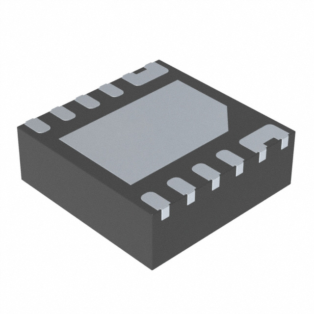
3mm x 3mm DFN-12L Package
UL2367 file no. E326264
IEC60950 CB Certificate no. US-31249-UL
The AOZ1353DI has True Reverse-Current Blocking
(TRCB) protection to avoid undesired reverse-current
from VOUT to VIN.
The device features fast recovery to turn on power switch
once reverse current blocking protection is de-activated.
The AOZ1353DI is available in 3mm x 3mm DFN-12L
package.
Applications
USB PD power source switch
Smart phone and tablet
Notebook, ultrabook and desktop
Portable devices
Typical Application
VIN
VOUT
COUT
CIN
AOZ1353DI
ILIM
RLIM
RFLTB
FLTB
ON
OFF
Rev. 1.2 February 2018
EN
GND
SS
www.aosmd.com
CSS
Page 1 of 16
�AOZ1353DI
Ordering Information
Part Number
Fault Recovery
Package
Environmental
AOZ1353DI-01
Auto-Restart
3mm x 3mm DFN-12L
RoHS
AOZ1353DI-02
Latch-Off
3mm x 3mm DFN-12L
RoHS
All AOS products are offered in packages with Pb-free plating and compliant to RoHS standards.
Please visit www.aosmd.com/media/AOSGreenPolicy.pdf for additional information.
Pin Configuration
VOUT
`
VOUT
VOUT
VIN
VIN
EXP
FLTB
VIN
EN
SS
ILIM
NC
GND
3mm x 3mm DFN-12L
(Top Transparent View)
Pin Description
Pin Number
Pin Name
Pin Function
1, 2, 3
VOUT
Power output. Connect to adaptor. Pin 3 is internally connected to pin 1 and pin 2.
4
FLTB
Fault indicator, open-drain output, active-low when fault condition occurs.
5
SS
Soft-start pin. Connect a capacitor CSS from SS to GND to set the soft-start time or short to
GND for fixed-time soft-start.
Not connected internally. Can leave it floated or connect to GND.
6
NC
7
GND
Ground
8
ILIM
Current limit set pin. Connect a 1% resistor RLIM from ILIM to GND to set the current limit
threshold.
9
EN
Enable input. Active high.
10, 11, 12
VIN
Supply input. Connected to internal power regulator. Pin 10 is internally connected to pin 11
and pin 12.
EXP
EXP
Exposed pad. Connect to GND.
Rev. 1.2 February 2018
www.aosmd.com
Page 2 of 16
�AOZ1353DI
Absolute Maximum Ratings
Recommended Operating Ratings
Exceeding the Absolute Maximum Ratings may damage the
device.
The device is not guaranteed to operate beyond the Maximum
Operating Ratings.
Parameter
Rating
VOUT to GND
Parameter
-0.3V to +28V
VIN, EN, ILIM, SS, FLTB to GND
Junction Temperature (TJ)
VIN to GND
-0.3V to +6V
0V to 5.5V
Switch Current (ISW)
-65°C to +150°C
ESD Rating HBM/CDM
3.4V to 5.5V
EN, FLTB to GND
+150°C
Storage Temperature (TS)
Rating
0A to 3.5A
Ambient Temperature (TA)
±4kV / ±1kV
-40°C to +85°C
Package Thermal Resistance
50°C/W
Electrical Characteristics
TA = 25°C, VIN = 5V, SS pin is shorted to GND unless otherwise specified.
Symbol
Parameter
Conditions
Min.
Typ.
Max.
Units
5.5
V
3.35
V
General
VIN
Input Supply Voltage
3.4
VUVLO_R
Under-voltage Lockout Threshold
VIN rising
VUVLO_HYS
3
3.25
Under-voltage Lockout Hysteresis
VIN falling
150
mV
IIN_ON
Input Quiescent Current
VIN = 5V, IOUT = 0A, EN = 5V
80
µA
IIN_OFF
Input Shutdown Current
VIN = 5V, EN = 0V
0.1
Switch On Resistance
VIN = 5V, IOUT = 1A
40
RON
VEN_H
Enable Input Logic High Threshold
EN rising
VEN_L
Enable Input Logic Low Threshold
EN falling
IEN_BIAS
Enable Input Bias Current
EN = 1.8V
VFLTB_LO
FLTB Pull-down Voltage
ISINK = 3mA
1
µA
mΩ
1.4
V
1
0.4
V
1.5
µA
0.3
V
Over-Voltage Protection
VOVLO_R
VOVLO_F
Over-voltage Lockout Threshold
VOVLO_HYS
Over-voltage Lockout Hysteresis
TDELAY_OVP
OVP Turn-Off Delay
VIN rising
5.5
VIN falling
5.75
6
5.5
Time between VIN rises from 5V to
6.5V and power switch turns off
V
250
mV
2
µs
Over-Current Protection
VOUT = 5V, RLIM = 4.02kΩ
ILIM
TOCP_FLTB
Current Limit Threshold
Over-Current Flag Delay
3.08
3.5
3.92
VOUT = 5V, RLIM = 14.3kΩ
0.9
1
1.1
VOUT = 5V, RLIM = 29.4kΩ
0.45
0.5
0.55
A
From IOUT ≥ ILIM to FLTB pulled low
12
ms
Reverse-Current Blocking
VT_RCB
RCB Protection Trip Point
VOUT-VIN, VOUT rising
60
mV
VR_RCB
RCB Protection Release Trip Point
VIN-VOUT, VOUT falling
70
mV
RCB Hysteresis
VT_RCB + VR_RCB
130
mV
2
µs
VRCB_HYS
TRCB
RCB Response Time
Rev. 1.2 February 2018
www.aosmd.com
Page 3 of 16
�AOZ1353DI
Electrical Characteristics
TA = 25°C, VIN = 5V, SS pin is shorted to GND unless otherwise specified.
Symbol
Parameter
Conditions
Min.
Typ.
Max.
Units
Thermal Shutdown
TSD
Thermal Shutdown Threshold
Temperature rising
140
TSD_HYS
Thermal Shutdown Hysteresis
Temperature falling
20
Turn-On Delay Time (From VEN
50% to VOUT=0.5V)
VIN = 5V, RL = 100, COUT = 1F,
CSS = 1nF, RLIM = 14.3kΩ
2.1
ms
Turn-ON Time (VOUT from 0.5V to
4.5V)
VIN = 5V, RL = 100, COUT = 1F,
SS Pin grounded, RLIM = 14.3kΩ
3.4
ms
°C
Dynamic Characteristics
TD_ON
TON
Rev. 1.2 February 2018
www.aosmd.com
Page 4 of 16
�AOZ1353DI
Functional Block Diagram
VOUT
VIN
VCC
Gate Drive &
Charge Pump
SS
Current
Limit
VIN
VOUT
UVLO
OVLO
TRCB
Control Logic
ILIM
FLTB
EN
GND
Rev. 1.2 February 2018
www.aosmd.com
Page 5 of 16
�AOZ1353DI
Timing Diagrams
EN
TD_ON
VOUT
TON
Figure 1. Turn-on Delay and Turn-on Time
VIN
TDELAY_OVP
VOUT
Figure 2. OVP Delay and Recovery
Rev. 1.2 February 2018
www.aosmd.com
Page 6 of 16
�AOZ1353DI
Typical Performance Curves
TA = 25°C, COUT = 20µF, RLIM = 4.02k, SS pin shorted to GND unless otherwise specified.
Figure 3. Startup by EN (RLoad = 1.6Ω)
Figure 4. Shutdown by EN (RLoad = 1.6Ω)
Figure 5. Startup by VIN (RLoad = 1.6Ω)
Figure 6. Shutdown by VIN (RLoad = 1.6Ω)
Figure 7. Input Over-Voltage Protection and Recovery
(RLoad = 1kΩ, AOZ1353DI-01)
Figure 8. Over-Current Protection
(RLOAD = 1Ω, AOZ1353DI-01)
Rev. 1.2 February 2018
www.aosmd.com
Page 7 of 16
�AOZ1353DI
Typical Performance Curves (Continued)
TA = 25°C, COUT = 20µF, RLIM = 4.02k, SS pin shorted to GND unless otherwise specified.
Figure 9. Output Hard Short and Thermal Shutdown
(AOZ1353DI-01)
Rev. 1.2 February 2018
www.aosmd.com
Page 8 of 16
�AOZ1353DI
Typical Characteristics
55.0
48.0
50.0
46.0
45.0
44.0
RON (m)
RON (m)
TA = 25°C, VIN = 5V unless otherwise specified.
40.0
35.0
42.0
40.0
30.0
38.0
25.0
36.0
20.0
-50
-30
-10
10
30
70
50
34.0
3.0
90
3.5
4.0
5.5
6.0
0.8
100
Input Shutdown Current (µA)
90
Input Quiescent Current (µA)
5.0
Figure 11. RON vs. Input Voltage
Figure 10. RON vs. Temperature
80
70
60
50
40
30
20
10
0
-50
-30
-10
10
30
50
70
0.7
0.6
0.5
0.4
0.3
0.2
0.1
0.0
-50
90
-30
-10
Temperature (C)
10
30
50
70
90
Temperature (C)
Figure 12. Input Quiescent Current vs. Temperature
Figure 13. Input Shutdown Current vs. Temperature
1.5
1.2
1.4
Rising
1.0
Enable Bias Current (µA)
Enable Threshold Voltage (V)
4.5
Voltage (V)
Temperature (C)
Falling
0.8
0.6
0.4
0.2
1.3
1.2
1.1
1.0
0.9
0.8
0.7
0.0
-50
-30
-10
10
30
50
70
90
0.6
-50
Temperature (°C)
-10
10
30
50
70
90
Temperature (°C)
Figure 14. EN Threshold vs. Temperature
Rev. 1.2 February 2018
-30
Figure 15. EN Bias Current vs. Temperature
www.aosmd.com
Page 9 of 16
�AOZ1353DI
Typical Characteristics (Continued)
TA = 25°C, VIN = 5V unless otherwise specified.
5.80
3.20
5.75
Rising
OVP Threshold Voltage (V)
UVLO Threshold Voltage (V)
3.24
3.16
3.12
3.08
Falling
3.04
3.00
-50
Rising
5.70
5.65
5.60
5.55
Falling
5.50
5.45
-30
-10
10
30
50
70
5.40
-50
90
-30
-10
Figure 16. UVLO Threshold vs. Temperature
30
50
70
90
Figure 17. OVP Threshold vs. Temperature
4.0
3.5
10
Temperature (°C)
Temperature (°C)
80.0
RLIM = 4.02 k
70.0
3.0
VT_RCB (mV)
ILIM (A)
2.5
2.0
1.5
RLIM = 14.3 k
1.0
0.0
-50
-30
-10
10
30
50
70
50.0
40.0
30.0
RLIM = 29.4 k
0.5
60.0
20.0
-50
90
-30
-10
Temperature (°C)
80.0
2.70
70.0
2.50
60.0
50.0
40.0
30.0
-30
-10
10
30
50
70
90
50
70
90
2.30
2.10
1.90
1.70
1.50
-50
Temperature (°C)
-30
-10
10
30
50
70
90
Temperature (°C)
Figure 20. RCB Threshold (Falling) vs. Temperature
Rev. 1.2 February 2018
30
Figure 19. RCB Threshold (Rising) vs. Temperature
Turn-On Delay Time (ms)
VR_RCB (mV)
Figure 18. Current Limit Threshold vs. Temperature
20.0
-50
10
Temperature (°C)
www.aosmd.com
Figure 21. Turn-On Delay vs. Temperature
Page 10 of 16
�AOZ1353DI
Typical Characteristics (Continued)
TA = 25°C, VIN = 5V unless otherwise specified.
4.0
4.0
3.5
SS Pin Grounded
3.0
3.0
2.5
2.5
ILIM (A)
Turn-On Time (ms)
3.5
2.0
2.0
1.5
1.5
1.0
1.0
0.5
0.5
0.0
-50
-30
-10
10
30
50
70
90
0.0
Temperature (°C)
5
10
15
20
25
30
35
40
RLIM (k)
Figure 22. Turn-On Time vs. Temperature
Rev. 1.2 February 2018
0
Figure 23. Current Limit vs. RLIM
www.aosmd.com
Page 11 of 16
�AOZ1353DI
Functional Description
True Reverse-Current Blocking Protection (TRCB)
The AOZ1353DI is a current limited power switch with
over-voltage, over-current, reverse-current and thermal
shutdown protections. The VOUT pin is rated 28V. The
operating input voltage ranges from 3.4V to 5.5V. The
switch current is rated up to 3.5A.
True reverse-current blocking prevents undesired current
flow from output to input when power switch is in either on
or off state. When device is enabled, power switch is
quickly turned off whenever output voltage is higher than
input voltage. The power switch is turned on again when
output voltage falls below input by 70mV.
The device has true reverse-current blocking features
that will prevent undesired current flow from output to its
input in either enabled or disabled state.
Enable
The EN pin is the ON/OFF control for the power switch.
The device is enabled when EN pin is high and not in
under-voltage lockout state. The EN pin must be driven
to a logic high or logic low state to guarantee operation.
While disabled, the AOZ1353DI draws less than 1μA
from supply.
For AOZ1353DI-02, toggle EN pin to restart the device
and clear fault flag after device latches off due to fault.
Input Under-Voltage Lockout (UVLO)
The under-voltage lockout (UVLO) circuit monitors the
input voltage. The power switch is only allowed to turn on
when input voltage is higher than UVLO threshold.
Otherwise the switch is off.
Over-Voltage Protection (OVP)
The voltages at VIN terminal is constantly monitored
once the device is enabled. In case input voltage
exceeds the over-voltage lockout threshold (VOVLO_R),
the power switch is either turned off immediately or kept
off, depending on its initial state. AOZ1353DI-01 can
restart when VIN drops below VOVLO_F.
Fast Recovery (For AOZ1353DI-01 only)
Once RCB event is removed, power switch turns on again
quickly. The recovery time is less than 100µs.
Thermal Shutdown Protection
Thermal shutdown protects device from excessive temperature. The power switch is turned off when the die temperature reaches thermal shutdown threshold of 140°C.
There is a 20°C hysteresis. For AOZ1353DI-01 power
switch is allowed to turn on again if die temperature drops
below approximately 120°C.
Soft Start
The AOZ1353DI has soft-start circuitry to limit in-rush
current due to large capacitive load. By default the turn-on
time is 3.4ms when SS pin is connected to GND.
Fast turn-on time can be set by adding an external
capacitor CSS between SS pin and ground. The capacitor
value is selected using Table 1.
Table 1. Turn-On Time Settings by Css
Css (nF)
Turn-On Time (ms)
1
0.3
1.2
0.4
Programmable Current Limit and Over-Current
Protection (OCP)
2.2
0.8
3.3
1.2
The AOZ1353DI implemented current limit to ensure that
the current through the switch does not exceed current
limit threshold set by the external resistor RLIM.
4.7
1.7
5.6
1.9
The current limit threshold can be estimated using the
equation below:
6.8
2.4
8.2
2.8
10
3.2
12
3.4
SS pin short to GND
3.4
ILIM = 14300/RLIM (A)
For example, for 1A current limit threshold, a 14.3kΩ RLIM
resistor should be selected. 1% resistor is recommended
for RLIM.
AOZ1353DI continuously limits the output current when
output is overloaded, Under current-limiting, FLTB is
pulled low after delay (TOCP_FLTB). Severe overload
causes power dissipation and die temperature to increase
and may trigger thermal shutdown.
Rev. 1.2 February 2018
Startup
The device is enabled when EN ≥ VEN_H and input voltage
is above UVLO threshold. The device first checks if any
fault condition exists. When no fault exists, the power
switch is turned on and the output is then ramped up.
Power switch is kept off if fault condition was detected.
www.aosmd.com
Page 12 of 16
�AOZ1353DI
Fault Reporting
Output Capacitor Selection
AOZ1353DI protects itself and load from the following
fault condition: over-voltage, over-current, reversecurrent, and over-temperature.
The output capacitor acts in a similar way. Also, the
output capacitor has to supply enough current for a
large load that it may encounter during system
transient. This bulk capacitor must be large enough to
supply fast transient load in order to prevent the output
from dropping.
The FLTB pin is an open drain output. It is asserted low
when either an over-current, or over-temperature
condition occurs. The FLTB pin becomes high
impedance when the fault conditions are removed. A
pull-up resistor (RFLTB) must be connected between
FLTB to 5V to provide a logic signal.
When thermal shutdown is activated, FLTB is pulled low
immediately to report fault condition to host. FLTB is
pulled high once fault is removed.
There is an upper limit for output capacitor for
AOZ1353DI to ensure the output capacitor can be
charged fully during start-up. This upper limit is set by
the current limit level and soft-start time.
Cout = ILIM × (TON / VIN)
Power Dissipation Calculation
In case of output overload, FLTB pin is pulled low about
12ms (TOCP_FLTB) after device is in current- limiting. For
AOZ1353DI-02 power switch is then turned off after
another 12ms.
Calculate the power dissipation for normal load condition
using the following equation:
There is no fault reporting for UVLO, OVP and RCB
event.
The worst case power dissipation occurs when the load
current hits the current limit due to over-current. The
power dissipation can be calculated using the following
equation:
Auto-restart or Latch-off
Power Dissipated = RON × (IOUT)2
AOZ1353DI-01 (auto-restart version): The device will
try to restart 24ms after the power switch is turned off
and when OVP or thermal shutdown fault is removed.
Power Dissipated = (VIN – VOUT) × ILIM
Power switch is turned on immediately after a RCB event
is removed.
Good PCB layout is important for improving the thermal
and overall performance of AOZ1353DI. To optimize the
switch response time to output short-circuit conditions,
keep all traces as short as possible to reduce the effect
of unwanted parasitic inductance. Place the input and
output bypass capacitors as close as possible to the
VIN and VOUT pins. The input and output PCB traces
should be as wide as possible for the given PCB space.
Use a ground plane to enhance the power dissipation
capability of the device.
AOZ1353DI-02 (latch-off version): The device keeps off
even after the fault condition is removed. Power switch
can only be turned on again by either toggle EN pin or
recycle the input supply.
Input Capacitor Selection
The input capacitor prevents large voltage transients
from appearing at the input, and provides the instantaneous current needed each time the switch turns on to
charge output capacitors and to limit input voltage drop.
It is also to prevent high-frequency noise on the power
line from passing through to the output. The input
capacitor should be located as close to the pin as possible. A minimum of 10μF ceramic capacitor should be
used. However, higher capacitor value is strongly recommended to further reduce the transient voltage drop
at the input.
Rev. 1.2 February 2018
Layout Guidelines
www.aosmd.com
Page 13 of 16
�AOZ1353DI
Package Dimensions, DFN3x3B_12L, EP1_S
RECOMMENDED LAND PATTERN
SYMBOLS
UNIT: mm
A
A1
b
b1
c
D
D1
E
E1
e
L
L1
L2
aaa
bbb
ccc
ddd
DIMENSIONS IN MILLIMETERS
MIN
����
����
����
����
�����
����
����
����
����
����
����
����
NOM
����
����
����
����
�����
����
����
����
����
����%6&
����
����
����
����
����
����
����
DIMENSIONS IN INCHES
MAX
����
����
����
����
�����
����
����
����
����
MIN
�����
�����
�����
�����
�����
�����
�����
�����
�����
����
����
����
�����
�����
�����
NOM
�����
�����
�����
�����
�����
�����
�����
�����
�����
�����%6&
�����
�����
�����
�����
�����
�����
�����
MAX
�����
�����
�����
�����
�����
�����
�����
�����
�����
�����
�����
�����
NOTE
1. DIMENSIONING AND TOLERANCING CONFORM TO ASME Y14.5M-1994.
2. CONTROLLING DIMENSION IS MILLIMETER.
CONVERTED INCH DIMENSIONS ARE NOT NECESSARILY EXACT.
3. DIMENSION b APPLIES TO METALLIZED TERMINAL AND IS MEASURED BETWEEN
0.15mm. AND 0.30mm FROM THE TERMINAL TIP. IF THE TERMINAL HAS THE OPTIONAL
RADIUS ON THE OTHER END OF THE TERMINAL, THE DIMENSION b SHOULD NOT BE
MEASURED IN THAT RADIUS AREA.
4. COPLANARITY ddd APPLIERS TO THE TERMINALS AND ALL OTHER BOTTOM SURFACE
METALLIZATION.
Rev. 1.2 February 2018
www.aosmd.com
Page 14 of 16
�AOZ1353DI
Tape and Reel Drawing DFN3x3 EP
Carrier Tape
Reel
DFN3x3 EP TAPE
Leader / Trailer & Orientation
Rev. 1.2 February 2018
www.aosmd.com
Page 15 of 16
�AOZ1353DI
Part Marking
AOZ1353DI
(DFN3x3)
AG00
Option Code
Special Code
Part Number Code
YWLT
Year Code
Part Number
Week Code
Assembly lot Code
Description
Code
AOZ1353DI-01
Green Product
AG01
AOZ1353DI-02
Green Product
AG02
LEGAL DISCLAIMER
Applications or uses as critical components in life support devices or systems are not authorized. AOS does not
assume any liability arising out of such applications or uses of its products. AOS reserves the right to make
changes to product specifications without notice. It is the responsibility of the customer to evaluate suitability of the
product for their intended application. Customer shall comply with applicable legal requirements, including all
applicable export control rules, regulations and limitations.
AOS' products are provided subject to AOS' terms and conditions of sale which are set forth at:
http://www.aosmd.com/terms_and_conditions_of_sale
LIFE SUPPORT POLICY
ALPHA AND OMEGA SEMICONDUCTOR PRODUCTS ARE NOT AUTHORIZED FOR USE AS CRITICAL
COMPONENTS IN LIFE SUPPORT DEVICES OR SYSTEMS.
As used herein:
1. Life support devices or systems are devices or
systems which, (a) are intended for surgical implant into
the body or (b) support or sustain life, and (c) whose
failure to perform when properly used in accordance
with instructions for use provided in the labeling, can be
reasonably expected to result in a significant injury of
the user.
Rev. 1.2 February 2018
2. A critical component in any component of a life
support, device, or system whose failure to perform can
be reasonably expected to cause the failure of the life
support device or system, or to affect its safety or
effectiveness.
www.aosmd.com
Page 16 of 16
�


 工商网监
湘ICP备2023018690号
工商网监
湘ICP备2023018690号
