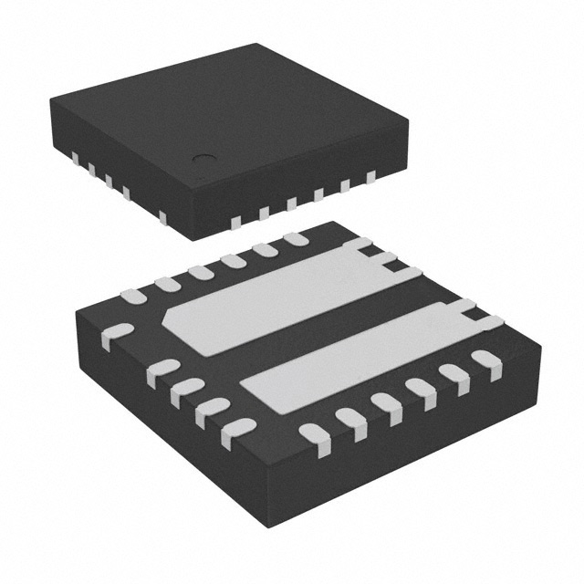
AOZ2234CQI-02
I2C Controllable 28V/10A Synchronous EZBuckTM Regulator
General Description
Features
The AOZ2234CQI-02 is an I2C controllable, high
efficiency, easy-to-use DC-DC synchronous buck
regulator capable of operation from a 6.5V to 28V input
bus. Ability to control the output voltage using the I2C bus
simplifies converter design for microprocessors or SoCs
that require dynamic voltage scaling or voltage
margining. The device is capable of supplying 10A of
continuous output current with an output voltage
adjustable from 1.790625V to 0.6V (±2.0%).
Wide input voltage range
The AOZ2234CQI-02 integrates an internal linear
regulator to generate 5.3V VCC from input. If input
voltage is lower than 5.3V, the linear regulator operates
at low drop output mode, which allows the VCC voltage is
equal to input voltage minus the drop-output voltage of
the internal linear regulator.
– 6.5V to 28V
10A continuous output current
Output voltage adjustable from 0.6V to 1.790625V in
9.375mV
±2.0% output voltage accuracy for I2C control
Low RDS(ON) internal NFETs
– 11m high-side
– 11m low-side
Constant On-Time with input feed-forward
Selectable PFM Light-Load Operation
Ceramic capacitor stable
Power Good output
A proprietary constant on-time PWM control with input
feed-forward results in ultra-fast transient response while
maintaining relatively constant switching frequency over
the entire input voltage range.
I2C address programming
The devices feature multiple protection functions such as
VCC under-voltage lockout, cycle-by-cycle current limit,
output over-voltage protection, short-circuit protection,
and thermal shutdown.
Over voltage protection
The AOZ2234CQI-02 is available in a 4mm×4mm QFN22L package and is rated over a -40°C to +85°C ambient
temperature range.
Applications
Integrated bootstrap diode
Cycle-by-cycle current limit
Short-circuit protection
Thermal shutdown
Thermally enhanced 4mm x 4mm QFN-22L package
Portable computers
Compact desktop PCs
Servers
Graphics cards
Set-top boxes
LCD TVs
Cable modems
Point-of-load DC/DC converters
Telecom/Networking/Datacom equipment
Rev 1.0 September 2018
www.aosmd.com
Page 1 of 23
�AOZ2234CQI-02
Typical Application
3.3V
R1
1.0k
R2
Off On
1.0k
EN
SCL
SCL
IN
0 6Ch
1 6Eh
µ Processor
POWER GOOD
5.3V
Analog Ground
Power Ground
AD0
BST
LX
AOZ2234CQI-02
R3
10k
C3
4.7µF
C1
20µF
VOUT
SDA
SDA
INPUT
6.5V to 28V
C4
0.1µF
VOUT
0.6V to 1.790625V
C2
110µF
L1
1.0µH
PGOOD
VCC
VOI
PGND
AGND
R4
R5
Option Table
Item
Code
AD0
Address
(Binary)
Address
(Hex)
Ground (0)
01101000
68h
Open (1)
01101010
6Ah
Ground (0)
01101100
6Ch
Open (1)
01101110
6Eh
AOZ2234CQI-01
AOZ2234CQI-02
Recommended Start-up Sequence
VIN
EN
50µs
Rev 1.0 September 2018
www.aosmd.com
Page 2 of 23
�AOZ2234CQI-02
Ordering Information
Part Number
Ambient Temperature Range
Package
Environmental
AOZ2234CQI-02
-40°C to +85°C
22-Pin 4mm x 4mm QFN
Green Product
AOS Green Products use reduced levels of Halogens, and are also RoHS compliant. Please visit
www.aosmd.com/media/AOSGreenPolicy.pdf for additional information.
Pin Configuration
LX
20
19
18
21
EN
VCC
22
BST
PGOOD
AD0
1
17
LX
SCL
2
16
LX
SDA
3
15
PGND
VOI
4
14
PGND
VOUT
5
13
PGND
AGND
6
12
PGND
8
9
10
11
IN
LX
LX
LX
IN
IN
7
IN
22-Pin 4mm x 4mm QFN
(Top View)
Rev 1.0 September 2018
www.aosmd.com
Page 3 of 23
�AOZ2234CQI-02
Pin Description
Pin Number
Pin Name
Pin Function
1
AD0
Chip Address. The AD0 pin just connects to AOZ2234CQI-02 VCC pin or GND.
2
SCL
Clock I/O Terminal.
3
SDA
Data I/O Terminal.
4
VOI
Initial Output Voltage Feedback Input. Adjust the output voltage with a resistive voltagedivider between VCC and AGND.
5
VOUT
Output Voltage Feedback Input. Connection to output voltage.
6
AGND
Analog Ground.
7, 8, 9
IN
Supply Input. IN is the regulator input. All IN pins must be connected together.
10, 11, 16, 17, 18
LX
Switching Node.
12, 13, 14, 15
PGND
Power Ground.
19
EN
Enable Input. The AOZ2234CQI-02 is enabled when EN is pulled high. The device shuts
down when EN is pulled low.
20
BST
Bootstrap Capacitor Connection. The AOZ2234CQI-02 includes an internal bootstrap
diode. Connect an external capacitor between BST and LX as shown in Typical
Application diagram.
21
VCC
Supply Input for Analog Functions. Bypass VCC to AGND with a 1µF~4.7µF ceramic
capacitor. Place the capacitor close to VCC pin.
PGOOD
Power Good Signal Output. PGOOD is an open-drain output used to indicate the status of
the output voltage. It is internally pulled low when the output voltage is 15% lower than the
nominal regulation voltage or 20% higher than the nominal regulation voltage. PGOOD is
pulled low during soft-start and shut down.
22
Rev 1.0 September 2018
www.aosmd.com
Page 4 of 23
�AOZ2234CQI-02
Absolute Maximum Ratings
Maximum Operating Ratings
Exceeding the Absolute Maximum Ratings may damage the
device.
The device is not guaranteed to operate beyond the
Maximum Operating ratings.
Parameter
Rating
IN to AGND
Parameter
Rating
-0.3V to 30V
Supply Voltage (VIN)
LX to AGND
-0.3V to 30V
Output Voltage Range
BST to AGND
-0.3V to 36V
Ambient Temperature (TA)
(1)
PGOOD, EN, VCC, SCL, SDA, VOUT, VOI,
AD0 to AGND
-0.3V to +0.3V
Junction Temperature (TJ)
+150°C
Storage Temperature (TS)
-65°C to +150°C
ESD Rating(2)
0.6 V to 1.790625V
-40°C to +85°C
Package Thermal Resistance
(JA)
(JC)
-0.3V to 6V
PGND to AGND
6.5V to 28V
32°C/W
4°C/W
2kV
Notes:
1. LX to PGND Transient (t
很抱歉,暂时无法提供与“AOZ2234CQI-02”相匹配的价格&库存,您可以联系我们找货
免费人工找货- 国内价格 香港价格
- 1+12.724741+1.52088
- 国内价格 香港价格
- 3000+5.416483000+0.64739
- 6000+5.115966000+0.61147
- 9000+4.964409000+0.59336
- 15000+4.7955515000+0.57317
