AOZ5048QI
High-Current, High-Performance
DrMOS Power Module
General Description
Features
The AOZ5048QI is a high efficiency synchronous buck
power stage module consisting of two asymmetrical
MOSFETs and an integrated driver. The MOSFETs are
individually optimized for operation in the synchronous
buck configuration. The high side MOSFET is optimized
to achieve low capacitance and gate charge for fast
switching with low duty cycle operation. The low side
MOSFET has ultra low ON resistance to minimize
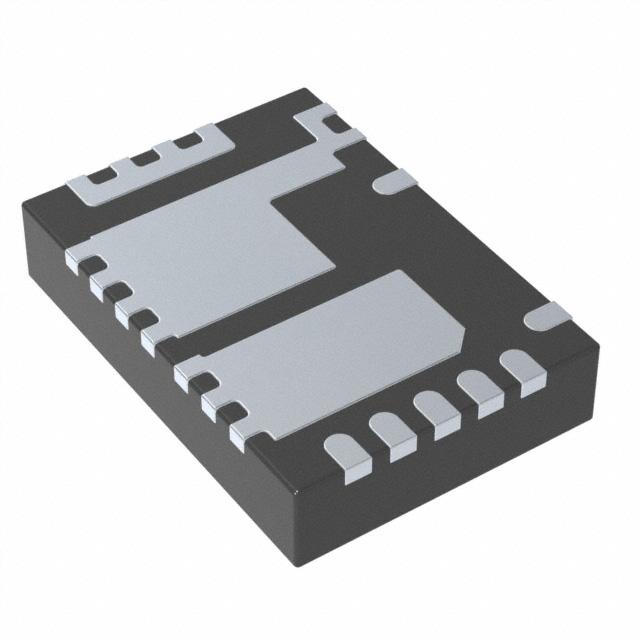
conduction loss. The compact 3.5mm x 5mm QFN
package is optimally chosen and designed to minimize
parasitic inductance for minimal EMI signature.
4.5V to 25V power supply range
The AOZ5048QI is intended for use with TTL and Tristate compatibility by using both the PWM and/or FCCM
inputs for accurate control of the power MOSFETs.
A number of features are provided making the
AOZ5048QI a highly versatile power module: The
bootstrap diode is integrated in the driver. The low side
MOSFET can be driven into diode emulation mode to
provide asynchronous operation when required. The pinout is optimized for low inductance routing of the
converter, keeping the parasitics and their effects to a
minimum.
4.5V to 5.5V driver supply range
Up to 35A peak output current
Integrated booststrap schottky diode
Up to 2MHz switching operation
Tri-state PWM input compatible
Under-Voltage LockOut protection
Single FCCM pin control for Shutdown / Diode
Emulation / CCM operation
Small 3.5mm x 5mm QFN-24L package
Applications
Servers
Notebook computers
VRMs for motherboards
Point of load DC/DC converters
Memory and graphic cards
Video gaming console
Typical Application Circuit
4.5V – 25V
VIN
BOOT
CBOOT
Controller
FCCM
Drive
Logic
and
Delay
VSWH
CVIN
VOUT
L
COUT
PWM
GL
PGND
Rev. 1.0 October 2016
PGND
VCC
+5V
CVCC
PGND
www.aosmd.com
PGND
Page 1 of 18
�AOZ5048QI
Ordering Information
Part Number
Ambient Temperature Range
Package
Environmental
AOZ5048QI
-40°C to +85°C
QFN3.5x5_24L
RoHS
AOS Green Products use reduced levels of Halogens, and are also RoHS compliant.
Please visit www.aosmd.com/media/AOSGreenPolicy.pdf for additional information.
4
VSWH
5
NC
VIN
PGND
GL
GL
PGND
PGND
18
17
GL
VIN
PGND
6
7
8
9
10
11
12
PGND
GH
19
PGND
3
20
PGND
BOOT
21
PGND
2
22
VIN
FCCM
23
VIN
1
24
VIN
PWM
VCC
Pin Configuration
16
VSWH
15
VSWH
14
VSWH
13
VSWH
QFN3.5X5_24L
(Top View)
Rev. 1.0 October 2016
www.aosmd.com
Page 2 of 18
�AOZ5048QI
Pin Description
Pin Number
Pin Name
Pin Function
1
PWM
PWM input signal from the controller IC. This input is compatible with 5V and Tri-State logic
levels.
2
FCCM
Continuous conduction mode of operation is allowed when FCCM = High. Discontinuous
mode is allowed and diode emulation mode is active when FCCM = Low. High impedance on
the input of FCCM will shutdown both High Side and Low Side MOSFETs.
3
BOOT
High Side MOSFET Gate Driver supply rail (5V with reference to VSWH). Connect a 100nF
ceramic capacitor between BOOT and the VSWH (Pin 5).
4
GH
5
VSWH
6, 7, 8
VIN
9, 10, 11, 12,
17, 18
PGND
13, 14, 15, 16
VSWH
High Side MOSFET Gate connection. This is for test purposes.
Switching node connected to the source of High Side MOSFET and the drain of Low Side
MOSFET. This pin is dedicated for booststrap capacitor connection to BOOT pin. It is required
to be connected to Pin 13 externally on PCB.
Power stage high voltage input pin.
Power Ground pin for power stage.
Switching node connected to the source of High Side MOSFET and the drain of Low Side
MOSFET. These pins are being used for Zero Cross Detect, Booststrap UVLO and Anti-Overlap Control.
19, 20
GL
21
PGND
Low Side MOSFET Gate connection. This is for test purposes.
22
VIN
Power stage high voltage input pin.
23
NC
Connect to Pin 24
24
VCC
Power Ground pin for Low Side MOSFET Gate Driver.
5V Power Pin for both the Bias Logic Blocks and HS and LS MOSFET Gate Driver Supply
Rail. Add a 4.7µF MLCC directly between Vcc (Pin 24) and PGND (Pin 21).
Functional Block Diagram
VCC
BOOT
VIN
VCC
FCCM
GH
REF/BIAS
/UVLO
Level
Translator
Control
Logic
HS
VCC
PWM
Tri-State
Clamps
Sequencing
and
Propagation
Delay Bank
Control
Logic
Driver
Logic
HS
Gate
Driver
HS
Output
Check
LS
MIN
ON
LS
VSWH
BST +
UVLO -
Voff
ZCD
Irev
PWM
Tri-State
Logic
PWM
+
-
DCM/CCM
Enable
Tri-State
SD
Logic
LS
Check
Tri-State
VCC
LS
Gate
Driver
GL
PGND
PGND
Rev. 1.0 October 2016
www.aosmd.com
Page 3 of 18
�AOZ5048QI
Absolute Maximum Ratings
Recommended Operating Conditions
Exceeding the Absolute Maximum ratings may damage
the device.
The device is not guaranteed to operate beyond the
Maximum Recommended Operating Conditions.
Parameter
Rating
Parameter
Low Voltage Supply (VCC)
-0.3V to 6V
High Voltage Supply (VIN)
-0.3V to 30V
-0.3V to (VCC+0.3V)
Control Inputs (PWM, FCCM)
Bootstrap Voltage DC
(BOOT-PGND)
-0.3V to 33V
Bootstrap Voltage DC
(BOOT-VSWH)
-0.3V to 6V
BOOT Voltage Transient(1)
(BOOT-VSWH)
-0.3V to 9V
Switch Node Voltage DC (VSWH)
-8V to 38V
High Side Gate Voltage DC (GH)
(VSWH-0.3V) to
BOOT
High Side Gate Voltage
Transient(1) (GH)
4.5V to 25V
Low Voltage Supply
{VCC, (BOOT-VSWH)}
4.5V to 5.5V
Control Inputs (PWM, FCCM)
0V to (VCC-0.3V)
Operating Frequency
200kHz to 2MHz
(VSWH-5V) to BOOT
Low Side Gate Voltage DC (GL)
(PGND-0.3V) to
(VCC+0.3V)
Low Side Gate Voltage
Transient(1) (GL)
(PGND-2.5V) to
(VCC+0.3V)
Storage Temperature (TS)
-65°C to +150°C
Max Junction Temperature (TJ)
ESD Rating
High Voltage Supply (VIN)
-0.3V to 30V
(1)
Switch Node Voltage Transient
(VSWH)
Rating
(2)
150°C
2kV
Notes:
1. Peak voltages can be applied for 20ns per switching cycle.
2. Devices are inherently ESD sensitive, handling precautions are
required. Human body model rating: 1k in series with 100pF.
Rev. 1.0 October 2016
www.aosmd.com
Page 4 of 18
�AOZ5048QI
Electrical Characteristics(3)
TA = 25°C, VIN = 12V, VCC = 5V unless otherwise specified.
Symbol
Parameter
VIN
Power Stage Power Supply
VCC
Driver Power Supply
RJC
RJA
Conditions
Min.
Typ.
4.5
VCC = 5V
Thermal Resistance
4.5
Max.
Units
25
V
5.5
V
PCB Temp = 100°C
3
°C/W
AOS Demo Board
10
°C/W
VCC Rising
3.5
INPUT SUPPLY AND UVLO
VCC
VCC_HYST
IVCC_SD
IVCC
Under-Voltage Lockout
VCC Falling
Under-Voltage Lockout Hysteresis
FCCM = Floating. VPWM = Floating
(internally pulled down)
FCCM = 5V, VPWM = Floating
(internally clamped to 2.5V)
FCCM = 0V, VPWM = Floating
(internally clamped to 2.5V)
Shutdown Bias Supply Current
Control Circuit Bias Current
3.9
V
3.1
V
400
mV
3
5
A
170
A
180
A
0.55
V
BOOTSTRAPPED DIODE
VF
Forward Current = 2mA
Forward Voltage
PWM INPUT
VPWMH
PWM Input High Threshold
VPWML
VPWM Rising, VCC = 5V
PWM Input Low Threshold
IPWM
PWM Pin Input Current
VTRI
PWM Input Tri-State Threshold Window
4.1
V
VPWM Falling, VCC = 5V
0.7
Source, VPWM = 5V
+200
Sink, VPWM = 0V
PWM = High Impedance
A
-200
1.5
V
A
3.3
V
FCCM INPUT
VFCCMH
FCCM Input High Threshold
VFCCML
FCCM Input Low Threshold
IFCCM
VTRI_HYST
VTRI
VTRI_CMLP
tPS4_EXIT
FCCM Rising, VCC = 5V
Shutdown → CCM
FCCM Falling, VCC = 5V
Shutdown → DCM
Source, FCCM = 5V
FCCM Pin Input Current
3.9
1.2
Sink, FCCM = 0V
Shutdown → CCM→ Shutdown
DCM → Shutdown → DCM
FCCM = High Impedance,
Shutdown Operation
FCCM Input Threshold Hysteresis
FCCM Input Tri-State Threshold Window
Tri-State Open Voltage
V
+50
A
-50
A
200
mV
2.1
3.1
V
15
s
2.5
PS4 Exit Latency
GATE DRIVER TIMING
tPDLU
PWM Falling to GH Turn-Off
V
V
VCC = 5V
5
PWM 10%, GH 90%
30
ns
25
ns
tPDLL
PWM Raising to GL Turn-Off
PWM 90%, GL 90%
tPDHU
GL Falling to GH Rising Deadtime
GL 10%, GH 10%
15
ns
tPDHL
GH/VSWH Falling to GL Rising Deadtime
VSWH @ 1V, GL 10%
13
ns
tTSSHD
Tri-State Shutdown Delay
TS to GH Falling, TS to GL Falling
150
ns
ns
ns
tPTS
Tri-State Propagation Delay
Tri-state exit, (see Figure 6)
45
tLGMIN
Low-Side Minimum On-Time
FCCM = 0V
350
Note:
3. All voltages are specified with respect to the corresponding PGND pin.
Rev. 1.0 October 2016
www.aosmd.com
Page 5 of 18
�AOZ5048QI
Timing Diagram
90%
PWM
10%
tPDHL
tPDLL
90%
GL
10%
10%
tPDLU
90%
GH
tPDHU
10%
VSWH
1V
Figure 1. PWM Logic Input Timing Diagram
PWM
tTSSHD
tTSSHD
tTSSHD
tTSSHD
GL
tPTS
tPTS
tPTS
tPTS
GH
Figure 2. Tri-State Input Logic Timing Diagram
Rev. 1.0 October 2016
www.aosmd.com
Page 6 of 18
�AOZ5048QI
CCM
FCCM
VTRIH
VTRIL
VFCCML
DCM
PWM
(Float)
VFCCMH
2.5V
Considering All Positive
(Forward Current)
In PS4 Mode
Shutdown
Delay
2.5V
PS4
Exit Delay
0V
tTPS
GL
tTPS
GL OFF
GH
GH OFF
Figure 3. FCCM Logic during High Impedance at PWM Input
Rev. 1.0 October 2016
www.aosmd.com
Page 7 of 18
�AOZ5048QI
Typical Performance Characteristics
TA = 25°C, VIN = 12V, VCC = 5V, unless otherwise specified.
Figure 4. Efficiency vs. Load Current
Figure 5. Power Loss vs. Load Current
90
7.5
VO = 1V, 35A, FSW = 800kHz
6.5
6.0
5.5
VIN = 19V
87
Power Loss (W)
Efficiency (%)
88
86
85
84
4.5
4.0
3.5
3.0
2.5
1.5
1.0
82
0.5
5
10
15
20
30
25
0
35
5
10
15
20
30
25
35
Load Current (A)
Load Current (A)
Figure 6. Supply Current vs. Switching Frequency
Figure 7. FCCM Input Threshold vs. Temperature
50
3.85
3.65
45
3.45
SD to CCM
CCM to SD
3.25
40
FCCM Threshold (V)
Supply Current (mA)
VIN = 19V
5.0
2.0
83
81
VO = 1V, 35A, FSW = 800kHz
7.0
89
35
30
25
3.05
2.85
FCCM Input
Threshold Window
2.65
2.45
2.25
2.05
DCM to SD
1.85
1.65
20
1.45
15
600
700
900
800
1000
1100
1200
1300
1400
1.25
-40
1500
SD to DCM
-20
0
20
Switching Frequency (kHz)
100
120
140
160
TS to PWM High
4.0
3.5
PWM High to TS
3.0
2.5
VCC - UVLO (V)
PWM Threshold (V)
80
3.6
4.5
PWM Input
Threshold Window
2.0
1.5
60
Figure 9. VCC UVLO vs. Temperature
Figure 8. PWM Threshold vs. Temperature
3.5
40
Temperature (°C)
PWM Low to TS
3.4
3.3
3.2
1.0
0.0
-60
3.1
TS to PWM Low
0.5
-40
-20
0
20
40
60
80
100
120
140
3.0
-60
Temperature (°C)
Rev. 1.0 October 2016
-40
-20
0
20
40
60
80
120
140
160
Temperature (°C)
www.aosmd.com
Page 8 of 18
�AOZ5048QI
Typical Performance Characteristics
TA = 25°C, VIN = 12V, VCC = 5V, unless otherwise specified.
Figure 10. VCC Shutdown Current vs. Temperature
Figure 11. PWM Threshold vs. VCC
5.0
4.0
4.5
2.5
2.0
1.5
1.0
3.5
3.0
2.5
2.0
1.5
PWM Low Threshold
1.0
0.5
0.0
PWM High Threshold
4.0
3.0
PWM Threshold (V)
VCC Shutdown Current (µA)
3.5
0.5
-60
-40
-20
0
20
40
60
80
100
120
140
0.0
4.0 4.1 4.2 4.3 4.4 4.5 4.6 4.7 4.8 4.9 5.0 5.1 5.2 5.3 5.4 5.5
Temperature (°C)
Rev. 1.0 October 2016
VCC (V)
www.aosmd.com
Page 9 of 18
�AOZ5048QI
Application Information
AOZ5048QI is a fully integrated power module designed
to work over an input voltage range of 4.5V to 25V with a
separate 5V supply for gate drive and internal control
circuits. A number of desirable features make
AOZ5048QI a highly versatile power module. The
MOSFETs are individually optimized for efficient operation
on either high side or low side switches in a low duty
cycle synchronous buck converter. A high current driver is
also integrated in the package which minimizes the gate
drive loop and results in extremely fast switching The
modules are fully compatible with Intel DrMOS
specification IMVP8 in form fit and function.
Powering the Module and the Gate Drives
An external supply VCC of 5V is required for driving the
MOSFETs. The MOSFETs are designed with low gate
thresholds so that lower drive voltage can be used to
reduce the switching and drive losses without
compromising the conduction losses. The integrated gate
driver is capable of supplying large peak current into the
Low Side MOSFET to achieve extremely fast switching. A
ceramic bypass capacitor of 4.7µF or higher is
recommended from VCC to PGND. For effective filtering it
is strongly recommended to directly connect this
capacitor to PGND (pin 21).
The BOOT supply for driving the High Side MOSFET is
generated by connecting a small capacitor (100nF)
between BOOT pin and the switching node VSWH (Pin
5). It is recommended that this capacitor Cboot be
connected as close as possible to the device across pins
3 and 5. Boost diode is integrated into the package. A
resistor in series with Cboot can be optionally used by
designers to slow down the turn on speed of the high
side MOSFET. Typically, values between 1Ω to 5Ω is a
compromise between the need to keep both the
switching time and VSWH node spikes as low as
possible.
Undervoltage Lockout
In a UVLO event, both GH and GL outputs are actively
held low until adequate gate supply becomes available.
The under-voltage lockout is set to 3.5V with a 400mV
hysteresis. The AOZ5048QI must be powered up before
the PWM input is applied.
Since the PWM control signals are provided typically from
an external controller or a digital processor, extra care
must be taken during start up. It should be ensured that
PWM signal goes through a proper soft start sequence to
minimize in-rush current through the converter during
start up. Powering the module with a full duty cycle PWM
signal may lead to a number of undesirable
Rev. 1.0 October 2016
consequences as explained below. In general it should be
noted that AOZ5048QI is a combination of two MOSFETs
with an IMVP8 compliant driver, all of which are optimized
for switching at the highest efficiency. Other than UVLO, it
does not have any monitoring or protection functions built
in. The PWM controller should be designed in to perform
these functions under all possible operating and transient
conditions.
Input Voltage VIN
AOZ5048QI is rated to operate over a wide input range of
4.5V to 25V. As with any other synchronous buck
converter, large pulse currents at high frequency and
extremely high di/dt rates will be drawn by the module
during normal operation. It is strongly recommended to
bypass the input supply very close to package leads with
X7R or X5R quality surface mount ceramic capacitors.
The high side MOSFET in AOZ5048QI is optimized for
fast switching with low duty ratios. It has ultra low gate
charges which have been achieved as a trade off with
higher RDS(ON) value. When the module is operated at
low VIN the duty ratio will be higher and conduction losses
in the HS MOSFET will also be correspondingly higher.
This will be compensated to some extent by reduced
switching losses. The total power loss in the module may
appear to be low even though in reality the HS MOSFET
losses may be disproportionately high. Since the two
MOSFETs have their own exposed pads and PCB copper
areas for heat dissipation, the HS MOSFET may be much
hotter than the LS MOSFET. It is recommended that worst
case junction temperature be measured and ensured to
be within safe limits when the module is operated with
high duty ratios.
PWM Input
AOZ5048QI is offered to interface with PWM logic
compatible with 5V (TTL). Refer to Fig. 1 for the timing
and propagation delays between the PWM input and the
gate drives.
The PWM is also a tri-state compatible input. When the
input is high impedance or unconnected both the gate
drives will be off and the gates are held active low. The
PWM Threshold Table in Table 1 lists the thresholds for
high and low level transitions as well as tri-state
operation. As shown in Fig. 2, there is a hold off delay
between the corresponding gate drive is pulled low. This
delay is typically 150ns and intended to prevent spurious
triggering of the tri-state mode which may be caused
either by noise induced glitches in the PWM waveform or
slow rise and fall times.
www.aosmd.com
Page 10 of 18
�AOZ5048QI
3. GH and GL follow PWM signal:
Table 1. PWM Input and Tri-State Thresholds
Thresholds
VPWMH
VPWML
VTRIH
VTRIL
PWM = Logic Hi GH = Hi, GL = Lo
AOZ5048QI
4.1 V
0.7 V
1.65 V
3.50 V
PWM = Logic Lo GH = Lo, GL = Hi
Note: See Figure 2 for propagation delays and tri-state window.
4. No detection for direction of inductor current
5. No detection for Voltage Level at VSWH node
Diode Mode Emulation of Low Side MOSFET (FCCM)
AOZ5048QI can be operated in the diode emulation or
skip mode using the FCCM pin. This is useful if the
converter has to operate in asynchronous mode during
start up, light load or under pre bias conditions. If FCCM
is taken high, the controller will use the PWM signal as
reference and generate both the high and low side
complementary gate drive outputs with the minimal
delays necessary to avoid cross conduction. When the
pin is taken low the HS MOSFET drive is not affected but
diode emulation mode is activated for the LS MOSFET.
See Table 2 for a comprehensive view of all logic inputs
and corresponding drive conditions. A high impedance
state at the FCCM pin shuts down the AOZ5048QI.
Function of FCCM When Signal is Rising
FCCM = 0V
1. The power stage is enabled and in DCM
(Discontinuous Conduction Mode).
2. GH and GL will follow PWM signal
3. Zero Current Detection (ZCD) is enabled. When
VSWH = 4mV and MIN_ON expires, ZCD will trigger
state machine to turn off GL. If VSWH reaches 4mV
before than MIN_ON, MIN_ON time takes priority and
will continue until this time period has completed.
Function of FCCM When Signal is Falling
FCCM = 5V 3.1V
1. Re-enter shutdown mode
2. Shutdown delay: 2.5µs
3. Occurs when Controller FCCM output enter high
impedance state
FCCM = Tri-State Window
(Ramp down window is 3.1 to 1.2V)
1. FCCM will be internally clamped to 2.5V
2. Remains in Shutdown Mode
FCCM = Tri-State 1.2V
(250 to 300mV lower than the DCM TS threshold)
1. Re-enable power stage
2. Controller pulls down on FCCM pin exiting shutdown
mode into DCM
3. Enable Delay: 5µs
4. Re-enable ZCD
Table 2. Control Logic Truth Table
FCCM
PWM
GH
GL
L
L
L
L (ZCD)
L
H
H
L
FCCM = 0V to 2.1V
1. GH and GL will turn off after shutdown delay (2.5µs).
FCCM = Tri-State Window
1. Input to FCCM is high impedance.
2. An internal buffer clamps FCCM to 2.5V.
3. GH and GL remain Off and ignore PWM signal.
FCCM = Tri-State to 3.9V (Fast Ramping)
1. The power stage is in CCM (Continuous Conduction
Mode)
2. GH and GL will follow PWM command
3. ZCD: is disabled
H
L
L
H
H
H
H
L
L
Tri-State
L
L
H
Tri-State
L
L
Tri-State
X
L
L
Note: Diode emulation mode is activated when FCCM pin is held low.
FCCM = 5V
1. The power stage is in CCM (Continuous Mode of
Operation)
2. Zero Current Detection (ZCD) is disabled
Rev. 1.0 October 2016
www.aosmd.com
Page 11 of 18
�AOZ5048QI
FCCM Timing Diagram and Truth Table
Controller Supply Rail
FCCM Input Rising
TS (Shutdown) to
FCCM Hi
FCCM Input Falling
VTRIH
VFCCMH
FCCM Hi to TS
(Shutdown)
VTRI_CMLP
VFCCML
VTRIL
(FCCM Low to TS
(Shutdown)
0V
TS (Shutdown) to
FCCM Low
0V
SHUTDOWN MODE
VCC
VCC
CCM Operation
CCM Operation
VTRIH
VFCCMH
VTRI_CLMP
SHUTDOWN MODE
FCCM Tri-State
Threshold Window
VTRI_CLMP
SHUTDOWN MODE
VFCCML
VTRIL
DCM Operation
DCM Operation
0V
0V
FCCM
ZCD
0V
0V
PWM
VSWH
GH
GL
Main Inductor Current Direction
L