AOZ6238
0.35 Low-Voltage Dual SPDT Analog Switch
General Description
Features
The AOZ6238 is a 0.35 Ω low-voltage Dual Single Pole
Double Throw (SPDT) analog switch. The AOZ6238
operates from a single 1.65 V to 4.3 V supply. It features
an ultra-low On Resistance of 0.35 Ω at a +3.0 V supply
and 25 °C. The AOZ6238 is designed for break-beforemake operation.
Typical 0.35
0.15
Ω On Resistance (RON) for +3.0 V supply
Ω maximum RON flatness for +3.0 V supply
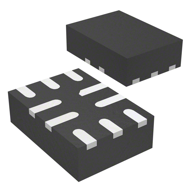
Package Options:
– TQFN-10: 1.8 mm x 1.4 mm x 0.55 mm package
– QFN-10: 1.8 mm x 1.4 mm x 0.75 mm package
Broad VCC operating range: 1.65 V to 4.3 V
High current handling capability (350 mA continuous
current under 3.3 V supply)
Internal 225
Ω resistor for “pop” free switching
Applications
Cell phone
PDA
Portable media player
Typical Application
Pin Configuration
AOZ6238
1B0
1B0
1A
1B1
1B1
1S
1S
Integrated
Base Band
Processor
GND
GND
2B0
2B0
2A
2B1
2B1
2S
2S
GND
GND
Rev. 2.0 December 2011
www.aosmd.com
Page 1 of 12
�AOZ6238
Ordering Information
Part Number
Ambient Temperature Range
Package
Environmental
AOZ6238QT
-40 °C to +85 °C
TQFN-10
RoHS Compliant
Green Product
AOZ6238QI
QFN-10
AOS Green Products use reduced levels of Halogens, and are also RoHS compliant.
Please visit www.aosmd.com/web/quality/rohs_compliant.jsp for additional information.
Pin Configuration
1S
2S
7
6
1A
8
5
2A
Vcc
9
4
GND
1B0
10
3
2B1
1
2
1B1
2B0
TQFN-10 / QFN-10
(Top Thru View)
Pin Description
Truth Table
Pin Name
Function
Logic Input
Function
1A, 2A, 1B0, 1B1, 2B0, 2B1
Data Ports
0
B0 Connected to A
1S, 2S
Control Input
1
B1 Connected to A
Rev. 2.0 December 2011
www.aosmd.com
Page 2 of 12
�AOZ6238
Absolute Maximum Ratings
Exceeding the Absolute Maximum ratings may damage the device.
Symbol
VCC
VSW
Parameter
Rating
Supply Voltage
Switch Voltage
-0.5 V to +5.5 V
(1)
-0.5 V to VCC + 0.5 V
(1)
VIN
Input Voltage
IIK
Minimum Input Diode Current(2)
-50 mA
ISW
Switch Current
350 mA
Peak Switch Current (Pulsed at 1 ms duration, 50
MHz
THD
Total Harmonic
Distortion
RL = 32 Ω, VIN = 2 Vpk-pk,
f = 20 Hz to 20 kHz
2.7 to 4.3
0.01
%
Q
Capacitance
Symbol
Parameter
Conditions
VCC (V)
CIN
Control Pin Input Capacitance
f = 1 MHz Vbias = 1.5 V
0.0
2
pF
COFF
B Port Off Capacitance
f = 1 MHz Vbias = 1.5 V
3.3
15
pF
CON
A Port On Capacitance
f = 1 MHz Vbias = 1.5 V
3.3
110
pF
Rev. 2.0 December 2011
www.aosmd.com
Min.
Typ.
Max.
Units
Page 5 of 12
�AOZ6238
Typical Performance Characteristics
RDS(on) vs. Analog Voltage @ 85 °C
2.0
1.8
1.8
RDS(on) - Drain-Source On Resistance (mΩ)
RDS(on) - Drain-Source On Resistance (mΩ)
RDS(on) vs. Analog Voltage @ 25 °C
2.0
1.6
Vcc =
1.65V
1.4
1.2
2.3V
1.0
2.7V
0.8
3.0V
0.6
4.3V
0.4
0.2
0.0
1.6
Vcc =
1.65V
1.4
1.2
1.0
2.3V
0.8
2.7V
3.0V
0.6
0.4
0.2
0.0
0
0.5
1.0
1.5 2.0 2.5 3.0
VD - Analog Voltage (V)
3.5
4.0
4.5
0
Crosstalk and Off Isolation vs. Frequency
0
-10
-1
-20
-2
-30
-40
-50
0.5
1.0
1.5 2.0 2.5 3.0
VD - Analog Voltage (V)
3.5
4.0
4.5
Insertion Loss vs. Frequency
0
Insertion Loss (db)
Xtalk, OIRR (db)
4.3V
-3
-4
-5
Xtalk
-6
-60
-7
-70
Off Isolation
-80
0.01
0.1
1
10
100
-8
0.1
Rev. 2.0 December 2011
1
10
100
1000
Frequency (MHz)
Frequency (MHz)
www.aosmd.com
Page 6 of 12
�AOZ6238
AC Loading and Waveforms
Vcc
Control
Input
VOUT
VB
RL
50Ω
t
Vcc
R = t F = 2.5nS
50%
0V
t OFF
CL
35pF
VOUT
Switch
Output
GND
0.9 x VOUT
0.9 x VOUT
0
t ON
Logic input waveform are inverted for switches with opposite
logic sense
CL Includes Fixture and Stray Capacitance
Figure 1. Turn-On/Turn-Off Timing
Vcc
B0
VB
Vcc
A
B1
VOUT
RL
50 Ω
S
CL
35pF
GND
Control
Input
50%
0V
t
R = t F = 2.5nS
VOUT
0.9 x VOUT
tD
CL Includes Fixture and Stray Capacitance
Figure 2. Break-Before-Make Timing`
Network
Analyzer
Vcc
B0
VIN
VOUT
50Ω
A
Network
Analyzer
Vcc
B0
50Ω
Source
Signal
B1
A
VIN
VOUT
50Ω
Source
Signal
50Ω
S
Vcc or 0V
+
S
50Ω
50Ω
GND
GND
Figure 4. Crosstalk
Figure 3. Off Isolation
Rev. 2.0 December 2011
Vcc or 0V
+
www.aosmd.com
Page 7 of 12
�AOZ6238
AC Loading and Waveforms (continued)
Vcc
R GEN
A
B 0 or B 1
V GEN
Input
Control
VOUT
VOUT
CL
IN
Δ VOUT
OFF
OFF
ON
S
GND
ON
OFF
IN
OFF
Q = (ΔVOUT)(CL)
Figure 5. Charge Injection
Vcc
10nF
Vcc
Network Analyzer
50Ω
BN
A
A
S
Capacitance
Meter
f = 1MHz
B 0 or B1
Source
Signal
0V
or
Vcc
S
+
50Ω
GND
GND
Figure 6. ON/Off Capacitance Measurement
Figure 7. Bandwidth
Vcc
Audio Analyzer
600 Ω
A
BN
32Ω
Source
Signal
CL
S
+
600 Ω
GND
CL Includes Fixture and Stray Capacitance
Figure 8. Harmonic Distortion
Rev. 2.0 December 2011
www.aosmd.com
Page 8 of 12
�AOZ6238
Package Dimensions, TQFN 1.8 x 1.4 x 0.55, 10L
E
e
L (x9)
Pin #1 ID
0.1 x 45°
e
Pin #1 Dot
by Marking
D
L1
Top View
b (x10)
Bottom View
A
c
A1
Side View
Dimensions in millimeters
RECOMMENDED LAND PATTERN
2.00
1.00
0.60
0.50
0.40
0.20
1.60
0.40
0.50
Symbols
A
A1
b
c
D
E
e
L
L1
Min.
0.50
0.00
0.15
Nom. Max.
0.55
0.60
—
0.05
0.20
0.25
0.152 REF.
1.35
1.40
1.45
1.75
1.80
1.85
0.40 BSC
0.35
0.40
0.45
0.50 REF.
Dimensions in inches
Symbols
A
A1
b
c
D
E
e
L
L1
Min.
Nom. Max.
0.020 0.022 0.024
0.000
—
0.002
0.006 0.008 0.010
0.006 REF.
0.053 0.055 0.057
0.069 0.071 0.073
0.016 BSC
0.014 0.016 0.018
0.020 REF.
1.00
0.60
0.50
0.20
0.20
UNIT: mm
Notes:
1. Controlling dimension is millimeter. Converted inch dimensions are not necessarily exact.
2. Angles are in degrees.
Rev. 2.0 December 2011
www.aosmd.com
Page 9 of 12
�AOZ6238
Package Dimensions, QFN 1.8 x 1.4B x 0.75, 10L
e
E
Pin #1 ID
0.1 x 45°
L (x9)
e
D
Pin #1 Dot
by Marking
L1
Top View
b (x10)
Bottom View
A
Side Vew
A1
c
Dimensions in millimeters
RECOMMENDED LAND PATTERN
2.00
0.50
1.00
0.60
0.40
0.20
1.00
1.60
Nom.
0.75
—
Min.
0.70
0.00
b
c
D
E
e
0.15
0.20
0.25
0.203 REF.
1.35
1.40
1.45
1.75
1.80
1.85
0.40 BSC
b
c
D
E
e
0.006 0.008 0.010
0.008 REF.
0.053 0.055 0.057
0.069 0.071 0.073
0.016 BSC
L
L1
0.35
0.45
L
L1
0.014
0.018
0.40
0.50
Max.
0.80
0.05
Dimensions in inches
Symbols
A
A1
0.45
0.55
Symbols
A
A1
Min.
0.028
0.000
Nom.
0.030
—
0.016
0.020
Max.
0.031
0.002
0.018
0.022
0.50
0.40
0.50 0.60
0.20
0.20
UNIT: mm
Notes:
1. Controlling dimension is millimeter. Converted inch dimensions are not necessarily exact.
2. Angles are in degrees.
Rev. 2.0 December 2011
www.aosmd.com
Page 10 of 12
�AOZ6238
Tape and Reel Dimensions, TQFN / QFN
Carrier Tape
D0
P1
D1
E1
K0
E2
E
B0
P2
P0
T
Feeding Direction
A0
UNIT: mm
Package
QFN 1.8 x 1.4
A0
1.90
±0.05
B0
1.70
±0.05
K0
D0
D1
1.00
1.50
0.50
±0.05 +0.10/-0 ±0.05
E
E1
8.00
1.75
+0.20/-0.10 ±0.10
E2
3.50
±0.05
P0
4.00
±0.10
P1
P2
4.00
2.00
±0.10 ±0.05
T
0.254
±0.02
Reel
W1
S
G
N
M
K
V
H
R
W
UNIT: mm
Tape Size Reel Size
8mm
ø178
M
ø178.0
±1.0
N
ø70.5
±1.0
W
9.0
±0.5
W1
11.8
±1.1
H
ø13.0
+0.5/-0.2
K
10.25
±0.1
S
2.4
±0.1
G
ø9.8
R
N/A
V
N/A
Leader/Trailer and Orientation
Trailer Tape
300mm min.
Rev. 2.0 December 2011
Components Tape
Orientation in Pocket
www.aosmd.com
Leader Tape
500mm min.
Page 11 of 12
�AOZ6238
Part Marking
AOZ6238QT
(TQFN-10)
AOZ6238QT
Product Number Code
D36
Assembly Lot Code and
Assembly Location Code
Week Code and
Year Code
AOZ6238QI
(QFN-10)
AOZ6238QI
Product Number Code
B36
Assembly Lot Code and
Assembly Location Code
Week Code and
Year Code
This datasheet contains preliminary data; supplementary data may be published at a later date.
Alpha & Omega Semiconductor reserves the right to make changes at any time without notice.
LIFE SUPPORT POLICY
ALPHA & OMEGA SEMICONDUCTOR PRODUCTS ARE NOT AUTHORIZED FOR USE AS CRITICAL
COMPONENTS IN LIFE SUPPORT DEVICES OR SYSTEMS.
As used herein:
1. Life support devices or systems are devices or
systems which, (a) are intended for surgical implant into
the body or (b) support or sustain life, and (c) whose
failure to perform when properly used in accordance
with instructions for use provided in the labeling, can be
reasonably expected to result in a significant injury of
the user.
Rev. 2.0 December 2011
2. A critical component in any component of a life
support, device, or system whose failure to perform can
be reasonably expected to cause the failure of the life
support device or system, or to affect its safety or
effectiveness.
www.aosmd.com
Page 12 of 12
�
很抱歉,暂时无法提供与“AOZ6238QT#A”相匹配的价格&库存,您可以联系我们找货
免费人工找货