0.3
General Description
AOZ6274
Low-Voltage Dual-DPDT Analog Switch
Features
The AOZ6274 is a dual Double-Pole, Double-Throw
(DPDT) analog switch that is designed to operate from
a single 1.65V to 4.3V supply. The AOZ6274 features
an ultra-low on resistance, excellent total harmonic
distortion (THD) performance, and low power
consumption. The device also features fast switching
and guaranteed Break-Before-Make (BBM) switching,
assuring the switches never shorts the driver.
Low On Resistance (RON) for +2.7V supply (0.3 )
Low ICCT current when nS input is lower than VCC
0.25
maximum RON flatness for +2.7V supply
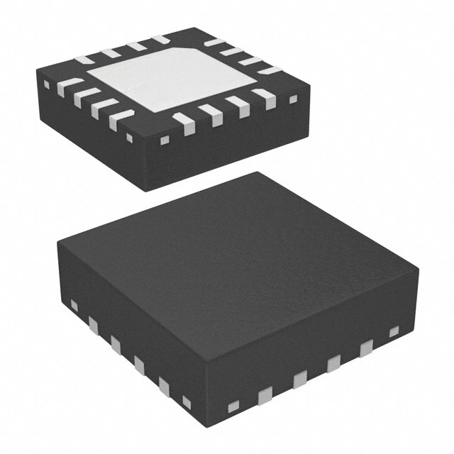
Small 3 x 3mm 16-Lead QFN Package
Broad 1.65V to 4.30V VCC operating range
Low THD (0.01% typical for 32
load)
Applications
Cell phone
PDA
Portable media player
Typical Application
Pin Configuration
�&�
�%
�&�
0�
0�
0�
7XIVIS�14�
4PE]IV
�&�
�%
6�
6�
0�
�7
�&�
�&�
0�
6�
0�
-RXIKVEXIH�
&EWIFERH
4VSGIWWSV 6�
�&�
6�
�&�
�7
6�
Rev. 1.5 February 2010
�7
www.aosmd.com
�%
�%
�&�
�7
Page 1 of 9
�AOZ6274
Ordering Information
Part Number
Ambient Temperature Range
Package
Environmental
AOZ6274QI
-40°C to +85°C
3x3 16-Lead QFN
Green
AOS Green Products use reduced levels of Halogens, and are also RoHS compliant.
Please visit www.aosmd.com/web/quality/rohs_compliant.jsp for additional information.
Pin Configuration
Pin Description
�&�
�
��
�%
�7
�
��
�&�
�&�
�
��
�7
�%
�
�
�&�
Pin Name
Function
1A, 2A, 3A, 4A, 1B0, 1B1, 2B0, 2B1,
3B0, 3B1, 4B0, 4B1
Data Ports
1S, 2S
Control Input
Truth Table
Logic Input
5*2���
�8ST�8LVY�:MI[
Function
0
nB0 Connected to nA
1
nB1 Connected to nA
Absolute Maximum Ratings
Exceeding the Absolute Maximum ratings may damage the device.
Symbol
Parameter
Rating
VCC
Supply Voltage
-0.5V to +4.6V
VS
Switch Voltage
-0.5 to VCC + 0.3V
VIN
Input Voltage
IIK
Minimum Input Diode Current
-50mA
ISW
Switch Current
350mA
ISWPEAK
TSTG
-0.5V to +4.6V
Peak Switch Current (Pulsed at 1ms duration, 55
MHz
THD
Total Harmonic
Distortion
RL = 32 , VIN = 2Vpp, f = 20Hz to 20kHz
3.6 to 4.3
0.01
%
2.7 to 3.6
0.01
2.3 to 2.7
0.01
Capacitance
Unless otherwise indicated, specifications indicate a temperature range of -40°C to +85°C.
All typical values are at 25°C unless otherwise specified.
Symbol
CIN
Parameter
Conditions
VCC (V)
Min.
Typ.
Max.
Units
Control Pin Input Capacitance
f = 1MHz
0.0
2.0
pF
COFF
B Port Off Capacitance
f = 1MHz
3.3
16
pF
CON
A Port On Capacitance
f = 1MHz
3.3
116
pF
Rev. 1.5 February 2010
www.aosmd.com
Page 4 of 9
�AOZ6274
AC Loading and Waveforms
:GG
'SRXVSP�
-RTYX
:398
:&
60
��
X
:GG
6 ! X * ! ���R7
��
�:
X 3**
'0
��T*
:398
7[MXGL�
�
3YXTYX
+2(
����\�:398
����\�:398
X 32
0SKMG�MRTYX�[EZIJSVQ�EVI�MRZIVXIH�JSV�W[MXGLIW�[MXL�STTSWMXI�
PSKMG�WIRWI
'0�-RGPYHIW�*M\XYVI�ERH�7XVE]�'ETEGMXERGI
*MKYVI����8YVR�3R�8YVR�3JJ�8MQMRK
:GG
&�
:&
%
&�
:398
60
��
7
'0
��T*
'SRXVSP�
-RTYX
:GG
��
�:
X
6 ! X * ! ���R7
:398
+2(
����\�:398
X(
'0�-RGPYHIW�*M\XYVI�ERH�7XVE]�'ETEGMXERGI
*MKYVI����&VIEO�&IJSVI�1EOI�8MQMRKD
2IX[SVO
%REP]^IV
:GG
&�
:-2
:398
��
%
2IX[SVO
%REP]^IV
:GG
&�
��
7SYVGI
7MKREP
&�
%
:-2
:398
��
7SYVGI
7MKREP
��
7
:GG�SV��:
�
7
��
:GG�SV��:
�
��
+2(
+2(
*MKYVI����'VSWWXEPO
*MKYVI����3JJ�-WSPEXMSR
Rev. 1.5 February 2010
www.aosmd.com
Page 5 of 9
�AOZ6274
AC Loading and Waveforms (continued)
:GG
6
+)2
%
& � SV & �
: +)2
-RTYX�
'SRXVSP
:398
:398
'0
-2
:398
3**
7
3**
32
+2(
32
3**
-2
3**
5�!�� :398
�'0
*MKYVI����'LEVKI�-RNIGXMSR
:GG
��R*
:GG
2IX[SVO�%REP]^IV
��
&2
%
%
7
'ETEGMXERGI�
1IXIV
J�!��1,^
& � SV &�
7SYVGI
7MKREP
�:
SV
:GG
7
�
��
+2(
*MKYVI����32�3JJ�'ETEGMXERGI�1IEWYVIQIRX
+2(
*MKYVI����&ERH[MHXL
:GG
%YHMS�%REP]^IV
���
%
&2
��
7SYVGI
7MKREP
'0
7
�
���
+2(
'0�-RGPYHIW�*M\XYVI�ERH�7XVE]�'ETEGMXERGI
*MKYVI����,EVQSRMG�(MWXSVXMSR
Rev. 1.5 February 2010
www.aosmd.com
Page 6 of 9
�AOZ6274
Package Dimensions, QFN 3 x 3
)
4MR����(SX
F]�1EVOMRK
)�
0
��\
0�
4MR����-HIRXMJMGEXMSR
'LEQJIV�'������\���
0�
(�
(
���6IJ�
�\
I
F
834�:-);
I��
&38831�:-);
%�
%�
%
7-()�:-);
6)'311)2()(�0%2(�4%88)62
����
'�����\���
����
����
����
����
����
����
(MQIRWMSRW�MR�QMPPMQIXIVW
7]QFSPW
%
%�
F
%�
(
)
(�
)�
I
0
0�
1MR�
����
����
����
����
����
����
����
����
2SQ�
����
h
����
������6IJ�
����
����
����
����
�����&7'
����
������6IJ�
1E\�
����
����
����
����
����
����
����
����
(MQIRWMSRW�MR�MRGLIW
7]QFSPW
%
%�
F
%�
(
)
(�
)�
I
0
0�
2SQ� 1E\�
������ �����
�����
h
����� �����
������6IJ�
����� ����� �����
����� ����� �����
����� ����� �����
����� ����� �����
������&7'
����� ����� �����
������6IJ�
1MR�
�����
�����
�����
����
92-8��QQ
2SXI�
���'SRXVSPPMRK�HMQIRWMSR�MW�QMPPMQIXIV��GSRZIVXIH�MRGL�HMQIRWMSRW�EVI�RSX�RIGIWWEVMP]�I\EGX�
Rev. 1.5 February 2010
www.aosmd.com
Page 7 of 9
�AOZ6274
Tape and Reel Dimensions, QFN 3 x 3
'EVVMIV�8ETI
(�
(�
4�
)�
/�
)�
)
&�
8
4�
%�
4�
*IIHMRK�(MVIGXMSR
92-8��QQ
4EGOEKI
%�
(*2��\��)4 ����
����
&�
/�
(�
����
����
����
����
����
��������
(�
����
��������
)
)�
)�
4�
4�
4�
8
�����
�����
����
����
����
����
����
����
����
����
����
����
����
����
6IIP
;�
7
+
2
1
/
:
6
,
;
92-8��QQ
8ETI�7M^I 6IIP�7M^I
��QQ
���
1
�����
����
2
�����
����
;
�����
����
;�
�����
����
,
����
�����������
/
�����
7
����
����
+
h
6
h
:
h
0IEHIV�8VEMPIV�ERH�3VMIRXEXMSR
8VEMPIV�8ETI
���QQ�QMR�
Rev. 1.5 February 2010
'SQTSRIRXW�8ETI
3VMIRXEXMSR�MR�4SGOIX
www.aosmd.com
0IEHIV�8ETI
���QQ�QMR�
Page 8 of 9
�AOZ6274
Part Marking
%3>����5�5*2���
4VSHYGX�2YQFIV�'SHI
���
%WWIQFP]�0SX�'SHI
�������
Please)���&��
provide input
)\XIRWMSR�'SHI
3TXMSR�'SHI
;IIO�'SHI�ERH�=IEV�'SHI
%WWIQFP]�0SGEXMSR�'SHI
This datasheet contains preliminary data; supplementary data may be published at a later date.
Alpha & Omega Semiconductor reserves the right to make changes at any time without notice.
LIFE SUPPORT POLICY
ALPHA & OMEGA SEMICONDUCTOR PRODUCTS ARE NOT AUTHORIZED FOR USE AS CRITICAL
COMPONENTS IN LIFE SUPPORT DEVICES OR SYSTEMS.
As used herein:
1. Life support devices or systems are devices or
systems which, (a) are intended for surgical implant into
the body or (b) support or sustain life, and (c) whose
failure to perform when properly used in accordance
with instructions for use provided in the labeling, can be
reasonably expected to result in a significant injury of
the user.
Rev. 1.5 February 2010
2. A critical component in any component of a life
support, device, or system whose failure to perform can
be reasonably expected to cause the failure of the life
support device or system, or to affect its safety or
effectiveness.
www.aosmd.com
Page 9 of 9
�
很抱歉,暂时无法提供与“AOZ6274QI#A”相匹配的价格&库存,您可以联系我们找货
免费人工找货