AOZ9252DI
Single-Cell Battery Protection IC with Integrated MOSFET
General Description
Features
The AOZ9252DI is a battery protection IC with
integrated dual common-drain N-channel MOSFET.
The device includes accurate voltage detectors and
delay circuits, and is suitable for protecting single-cell
lithium-ion/lithium-polymer rechargeable battery packs
from overcharge, over-discharge, and over-current
conditions.
Integrated Common-Drain N-Channel MOSFET
23.8m (typ.) source to source on resistance
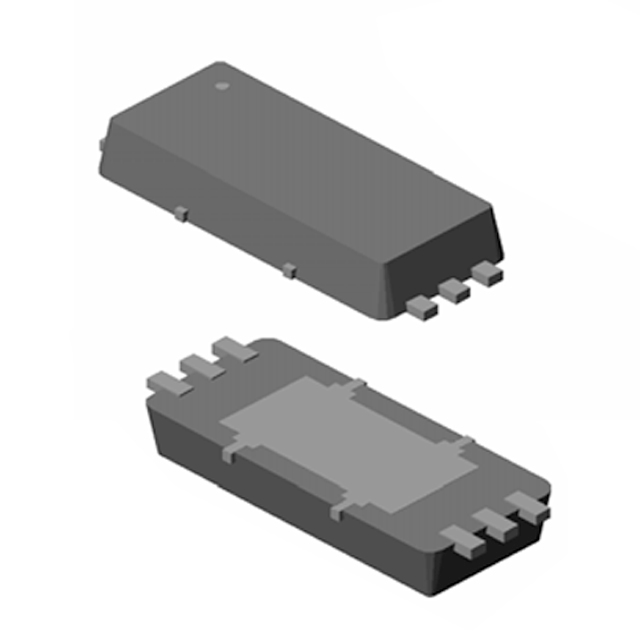
The AOZ9252DI is available in a 2mm x 4mm 6-pin DFN
package and is rated over a -40°C to +85°C ambient
temperature range.
High-accuracy voltage detection circuit
– Overcharge detection accuracy: 25mV (25°C),
45mV (-10°C to 60°C)
– Overcharge release accuracy: 40mV
– Over-discharge detection accuracy: 100mV
– Over-discharge release accuracy: 100mV
– Discharge over-current detection accuracy: 10mV
– Charge over-current detection accuracy: 15mV
20% accurate internal detection delay times
(external capacitors are unnecessary)
Charger connection pin withstands up to 24V
Wide operating temperature range: -40°C to 85°C
Low current consumption
– 2.8A (typ.), 5.0A (max.) in operation mode at
25°C
Small 2mm x 4mm 6-pin DFN package
Applications
Lithium-ion rechargeable battery packs
Lithium-polymer rechargeable battery
packs
Typical Applications Circuit
VSS
C1
0.1μF
EB+
NC
EB-
OUTM
AOZ9252DI
VDD
NC
R2
1kΩ
VM
R1
330Ω
Rev. 1.0 May 2014
www.aosmd.com
Page 1 of 16
�AOZ9252DI
Ordering Information
Part Number
OverOvercharge Overcharge discharge
Detection
Detection
Release
Voltage
Voltage
Voltage
(VDL)
(VCU)
(VCL)
AOZ9252DI
4.225V
4.025V
2.40V
Overdischarge
Release
Voltage
(VDU1)
Overdischarge
Release
Voltage
(VDU2)
2.80V
2.41V
Discharge Load Short- Charge
Overcircuiting
Overcurrent
Detection
current
Power 0V Battery
Threshold Threshold Threshold
Down
Charge
(VDIOV)*
(VSHORT)
(VCIOV)* Function Function
0.14V
0.50V
-0.15V
No
Yes
AOS Green Products use reduced levels of Halogens, and are also RoHS compliant.
Please visit www.aosmd.com/media/AOSGreenPolicy.pdf for additional information.
* Please refer to page 9 for calculation of charge and discharge current limit.
Table 1. Delay Time
Part Number
Overcharge
Detection
Delay Time
(tCU)
Over-discharge
Detection
Delay Time
(tDL)
Discharge
Over-current
Detection
Delay Time
(tDIOV)
Load Shortcircuiting
Detection
Delay Time
(tSHORT)
Charge
Over-current
Detection
Delay Time
(tCIOV)
AOZ9252DI
1.0s
64ms
8ms
250s
8ms
Pin Configuration
VSS
1
NC
2
VDD
3
PAD
6
OUTM
5
NC
4
VM
2x4 DFN-6
(Top View)
Pin Description
Pin Name
Pin
Number
Pin Function
NC
2, 5
VSS
1
Ground. VSS is the source of the internal Discharge MOSFET. Connect VSS directly to the cathode
of lithium-ion/lithium polymer battery cell.
VDD
3
Input supply pin. Connect a 0.1F capacitor between VDD and VSS.
VM
4
Over-current/Charger Detection Pin. Connect a 1k resistor between VM and the negative terminal
of the battery pack.
OUTM
6
Output pin. OUTM is the source of the internal Charge MOSFET. Connect OUTM directly to the
negative terminal of the battery pack.
PAD
Drain
MOSFET Common-Drain Connection. This pad is for test purposes only. Always leave this pad
unconnected.
Rev. 1.0 May 2014
Pin 2 is for test purposes only. Always leave pin 2 and pin 5 unconnected.
www.aosmd.com
Page 2 of 16
�AOZ9252DI
Functional Block Diagram
EB+
R1
330Ω
VDD
OverDischarge
Comp
Counter/
Logic
Oscillator
0V Battery
Charge
Function
VDD
Single-Cell
Lithium-Ion/
Lithium-Polymer
Battery
C1
0.1F
Over-Charge
Comp
VSS
Charge
Detection
Discharge
Over-Current
Comp
RVMD
VM
Charge
Over-Current
Comp
RVMS
Short-Circuit
Comp
R2
1kΩ
Battery Protection IC
DO
Discharge
FET
CO
Charge
FET
OUTM
EB-
Dual Common-Drain MOSFET
AOZ9252DI
Figure 1. AOZ9252DI Functional Block Diagram
Absolute Maximum Ratings
Exceeding the Absolute Maximum ratings may damage the device.
Ratings @ TA = 25°C, VSS = 0V
Symbol
Parameter
Conditions
Min.
Max.
Unit
VDD
Supply Voltage
–0.3
12
V
VM
VM Pin Voltage
VDD – 28
VDD + 0.3
V
24
V
6
A
VDSS
Drain-Source Voltage
ID
Current(1)
Drain
RJA = 90°C/W, TA =
25oC
TOPR
Operating Temperature
–40
85
°C
TSTD
Storage Temperature
–55
125
°C
0.8
W
PD
Total Power Dissipation(1)
RJA = 90°C/W, TA = 25oC
Note:
1.The value of RJA is measured with the device mounted on 1-in2 FR-4 board with 2-oz. copper, in a still air environment with
TA = 25°C. The value in any given application depends on the user’s specific board design.
Rev. 1.0 May 2014
www.aosmd.com
Page 3 of 16
�AOZ9252DI
Electrical Characteristics
TA = 25°C unless otherwise specified.
Control IC
Symbol
Parameter
Condition
Min.
Typ.
Max.
Unit
TA = 25°C
4.200
4.225
4.250
V
TA = -10°C to +60°C*
4.180
4.225
4.270
DETECTION VOLTAGE
VCU
Overcharge Detection Voltage
TA = -40°C to +85°C*
VCL
Overcharge Release Voltage
TA = 25°C
4.225
3.985
TA =-40°C to +85°C*
VDL
Over-discharge Detection Voltage
TA = 25°C
VDU1
Over-discharge Release Voltage 1
TA = 25°C
VDU2
Over-discharge Release Voltage 2
@VCHG = 4.2V, R1 = 330
2.300
2.400
2.700
2.800
Discharge Over-current threshold
2.310
2.410
Load Short-circuiting Detection
Voltage
TA = 25°C
VCIOV
Charge Over-current threshold
TA = 25°C
V
2.900
V
2.510
V
0.150
V
0.600
V
-0.135
V
2.410
0.130
TA = -40°C to +85°C*
VSHORT
2.500
2.800
TA = -40°C to +85°C*
TA = 25°C
V
2.400
TA = -40°C to +85°C*
VDIOV
4.065
4.025
TA = -40°C to +85°C*
TA = 25°C
4.025
0.140
0.140
0.400
0.500
-0.165
-0.150
TA = -40°C to +85°C*
0.500
TA = -40°C to +85°C*
-0.150
0V BATTERY CHARGE FUNCTION
V0CHA
Minimum 0V Battery Charge
Starter Battery Voltage
TA = 25°C, 0V battery charging function
available
1.9
TA = -40°C to +85°C*, 0V battery
charging function available
2.4
V
INPUT VOLTAGE
VDSOP1
Operating Voltage Between
VDD Pin and VSS Pin
Internal circuit operating voltage
1.5
6.5
V
VDSOP2
Operating Voltage Between
VDD Pin and VM Pin
Internal circuit operating voltage
1.5
28
V
Current Consumption During
Operation
VDD = 3.4V, VVM = 0V, TA = 25°C
1.0
2.8
5.0
VDD = 3.4V, VVM = 0V,
TA = -40°C to +85°C*
0.7
2.8
5.5
Over-discharge Current
Consumption
VDD = VVM = 1.5V, TA = 25°C
3.5
VDD = VVM = 1.5V, TA = 40°C to +85°C*
3.8
INPUT CURRENT
IOPE
IOPED
A
INTERNAL RESISTANCE
RVMD
Resistance Between VM Pin and
VDD Pin
VDD = 1.8V, VVM = 0V, TA = 25°C
100
300
900
VDD = 1.8V, VVM = 0V,
TA = -40°C to +85°C*
78
300
1310
k
*Parameters are guaranteed by design only and not production tested.
Rev. 1.0 May 2014
www.aosmd.com
Page 4 of 16
�AOZ9252DI
Electrical Characteristics (Continued)
TA = 25°C unless otherwise specified.
Control IC (Continued)
Symbol
RVMS
Parameter
Resistance Between VM Pin and
VSS Pin
Condition
Min.
Typ.
Max.
VDD = 3.4V, VVM=1.0V, TA = 25°C
10
20
30
VDD = 3.4V, VVM= 1.0V,
TA = -40°C to +85°C*
7.2
20
35
TA = 25°C
0.8
1.0
1.2
TA = -40°C to +85°C*
0.6
1.0
1.6
Unit
k
DETECTION DELAY TIME
tCU
tDL
tDIOV
tSHORT
tCIOV
Overcharge Detection Delay Time
Over-discharge Detection Delay
Time
TA = 25°C
51
64
77
TA = -40°C to +85°C*
38.4
64
102.4
Discharge Over-current Detection
Delay Time
TA = 25°C
6.4
8
9.6
TA = -40°C to +85°C*
4.8
8
12.8
Load Short-circuiting Detection
Delay Time
TA = 25°C
200
250
300
TA = -40°C to +85°C*
150
250
400
Charge Over-current Detection
Delay Time
TA = 25°C
6.4
8
9.6
TA = -40°C to +85°C*
4.8
8
12.8
s
ms
ms
s
ms
*Parameters are guaranteed by design only and not production tested.
Integrated MOSFET
Symbol
Parameter
BVDS_C
Charge Control MOSFET Drain-Source Breakdown
VDD = VCU
ILEAK_C
Charge Control MOSFET Leakage
VDD = VCU
BVDS_D
Discharge Control MOSFET Drain-Source
Breakdown Voltage
VDD = VDL
ILEAK_D
Discharge Control MOSFET Leakage Current
VDD = VDL
RSS
Condition
Total Output Resistance (OUTM to VSS)(2)
Min.
Typ.
Max.
Unit
1
A
24
V
24
V
1
A
VDD = 4.5V
19
23.8
29.8
m
VDD = 4.2V
19.3
24.1
30.2
m
VDD = 3.9V
19.8
24.4
30.5
m
VDD = 3.7V
20.1
24.8
31
m
VDD = 3.5V
20.5
25.1
32
m
VDD = 3.3V
21
26.3
32.9
m
VDD = 3.0V
22.1
27.6
34.5
m
VDD = 2.5V
25.8
32.2
41.9
m
*Parameters are guaranteed by design only and not production tested.
Rev. 1.0 May 2014
www.aosmd.com
Page 5 of 16
�AOZ9252DI
Electrical Characteristics (Continued)
TA = 25°C unless otherwise specified.
Discharge / Charge Overcurrent Characteristics
Symbol
IDIO
ICIO
Parameter
Discharge Overcurrent Detection Current
Charge Overcurrent Detection Current
Condition
Min.
Typ.
Max.
Unit
VDD = 4.2V
4.3
5.8
7.8
A
VDD = 3.9V
4.3
5.7
7.6
A
VDD = 3.7V
4.2
5.6
7.5
A
VDD = 3.5V
4.1
5.6
7.3
A
VDD = 3.3V
4.0
5.3
7.1
A
VDD = 3.0V
3.8
5.1
6.8
A
VDD = 4.2V
-4.5
-6.2
-8.5
A
VDD = 3.9V
-4.4
-6.1
-8.3
A
VDD = 3.7V
-4.4
-6.0
-8.2
A
VDD = 3.5V
-4.2
-6.0
-8.0
A
VDD = 3.3V
-4.1
-5.7
-7.9
A
VDD = 3.0V
-3.9
-5.4
-7.5
A
These parameters are calculated using the Current Limit Calculation; see item 7 in Theory of Operation section on page 9.
Rev. 1.0 May 2014
www.aosmd.com
Page 6 of 16
�AOZ9252DI
Theory of Operation
Please refer to the Timing Diagrams on page 10 for more information.
1. Normal Status
The AOZ9252DI monitors the voltage between the VDD
pin and VSS pin and the voltage difference between the
VM pin and VSS pin to control charging and discharging.
Since the device only draws a few microamperes of
current during operation and the voltage drop across the
low-pass filter R1 is negligible, the voltage between VDD
and VSS is equal to the battery voltage. When the battery
voltage is in the range between over-discharge detection
voltage (VDL) and overcharge detection voltage (VCU),
and the VM pin voltage is in the range between the
charge over-current detection voltage (VCIOV) and
discharge over-current detection voltage (VDIOV), the IC
turns both the charging and discharging control FETs on.
In this normal status, charging and discharging can be
carried out freely.
Caution:
Discharging may not be enabled when the battery is
connected for the first time. In this case,
1. Connect the charger or;
2. Set the VM pin’s voltage at the level of the charge
overcurrent detection voltage (VCIOV) or more and
the discharge overcurrent detection voltage (VDIOV)
or less by connecting the charger The IC returns to
the normal status.
2. Overcharge Status
When the battery voltage rises higher than overcharge
detection voltage (VCU) for the overcharge detection
delay time (tCU) or longer in the normal status, the
AOZ9252DI turns off the charging control MOSFET to
stop charging. This condition is the overcharge status.
The resistance (RVMD) between the VM pin and VDD pin,
and the resistance (RVMS) between the VM pin and VSS
pin are not connected. The overcharge status is released
in the following two cases:
1. In the case that the VM pin voltage is higher than or
equal to charge over-current (VCIOV), and is lower
than the discharge over-current detection voltage
(VDIOV), AOZ9252DI releases the overcharge status
when the battery voltage falls below the overcharge
release voltage (VCL).
When the discharge is started by connecting a load after
the overcharge detection, the VM pin voltage rises more
than the voltage at VSS pin due to the Vf voltage of the
parasitic diode. This is because the discharge current
flows through the parasitic diode in the charging control
FET. If this VM pin voltage is higher than or equal to the
discharge over current detection voltage (VDIOV),
AOZ9252DI releases the overcharge status when the
battery voltage falls below the overcharge detection
voltage (VCU).
For the actual application boards, changing the battery
voltage and the charger voltage simultaneously enables
to measure the overcharge release voltage (VCL). In this
case, the charger is always necessary to have the
equivalent voltage level to the battery voltage. The
charger keeps VM pin voltage higher than or equal to the
charge over-current detection voltage (VCIOV) and lower
than or equal to the discharge overcurrent detection
voltage (VDIOV). AOZ9252DI releases the overcharge
status when the battery voltage falls below overcharge
release voltage (VCL).
Cautions:
1. If the battery voltage is charged to a voltage higher
than overcharge detection voltage (VCU) and the
battery voltage doesn’t fall below overcharge
detection voltage (VCU) even when heavy load is
connected, discharge overcurrent detection and load
short-circuiting detection do not function until the
battery voltage falls below overcharge detection
voltage (VCU). Since an actual battery has an internal
impedance of tens of m, the battery voltage drops
immediately after a heavy load that causes over
current is connected, and discharge overcurrent
detection and load short-circuiting detection function.
2. When a charger is connected after overcharge
detection, the overcurrent status is not released even
if the battery voltage is below overcharge release
voltage (VCL). The overcharge status is released
when the VM pin voltage goes over charge
overcurrent detection voltage (VCIOV) by removing
the charger.
2. In the case that the VM pin voltage is higher than or
equal to the discharge over-current detection voltage
(VDIOV), AOZ9252DI releases the overcharge status
when the battery voltage falls below the overcharge
detection voltage (VCU).
Rev. 1.0 May 2014
www.aosmd.com
Page 7 of 16
�AOZ9252DI
3. Over-discharge Status
(Without Power-down Function)
When the battery voltage falls below overdischarge
detection voltage (VDL) during discharging in the normal
status and the detection continues for the overdischarge
detection delay time (tDL) or longer, AOZ9252DI turns the
control FET off to stop discharging. This condition is
called the overdischarge status. Under the overdischarge
status, the VM pin voltage is pulled up by the resistor
between the VM pin and VDD pin in the IC (RVMD).
When a battery in the overdischarge status is connected
to a charger and provided that the VM pin voltage is
lower than -0.7V (typ.), AOZ9252DI releases the
overdischarge status and turns the discharging FET on
when the battery voltage reaches overdischarge
detection voltage (VDL) or higher.
When a battery in the overdischarge status is connected
to a charger and provided that the VM voltage is not
lower than -0.7V (typ.), AOZ9252DI releases
overdischarge status when the battery voltage reaches
overdischarge release voltage (VDU) or higher.
4. Discharge Over-current Status
(Discharge Over-current, Load Short-circuiting)
When a battery is in the normal status, and the discharge
current becomes higher than specified value and the
status lasts for the discharge over-current detection delay
time (tDIOV), the IC turns off the discharge control
MOSFET and stops discharging. This status is called the
discharge over-current status. In the discharge overcurrent status, the VM pin and VSS pin are shorted by
the resistor between VM pin and VSS pin (RVMS) in the
IC. When the load is disconnected, the VM pin returns to
the VSS potential. When the impedance between the
EBpin and EB-pin (Refer to Figure 1) increases and is
equal to the impedance that enables automatic
restoration and the voltage at the VM pin returns to
discharge over-current detection voltage (VDIOV) or
lower, the discharge over-current status is restored to the
normal status. Even if the connected impedance is
smaller than automatic restoration level, the AOZ9252DI
will be restored to the normal status from discharge
over-current detection status when the voltage at the
VM pin becomes the discharge over-current detection
voltage (VDIOV) or lower by connecting the charger.
The resistance (RVMD) between the VM pin and VDD pin
is not connected in the discharge over-current detection
status.
Rev. 1.0 May 2014
When a battery is in the normal status, and the discharge
current becomes abnormally higher (EB+ pin and EB- pin
shorted), and thus the VM pin voltage is equal or higher
than load short-circuiting detection voltage (VSHORT) for
load short-circuiting detection delay time (tSHORT), the IC
turns off the discharge control MOSFET and stops
discharging. This status is the load shorting-circuiting
status. In the load shorting-circuiting status, the VM pin
and VSS pin are shorted by the resistor between VM pin
and VSS pin (RVMS) in the IC. When the short-circuiting
condition is released, the VM pin returns to the VSS
potential. The resistance (RVMD) between the VM pin and
VDD pin is not connected in the load shorting-circuiting
status.
When the battery voltage falls below overdischarge
detection voltage (VDL) due to overcurrent, the
AOZ9252DI turns the discharging control FET off via
overcurrent detection. In this case, if the recovery of the
battery voltage is so slow that the battery voltage after
the overdischarge detection delay time is still lower than
the overdischarge detection voltage, AOZ9252DI shifts to
the overdischarge status.
5. Charge Over-current Status
When a battery in the normal status is in the status, and
the charge current is higher than the specified value and
the status lasts for the charge over-current detection
delay time (tCIOV), the charge control MOSFET is turned
off and charging is stopped. This status is the charge
over-current status. This IC will be restored to the normal
status from the charge over-current status when, the
voltage at the VM pin returns to charge over-current
detection voltage (VCIOV) or higher by removing the
charger. The charge over-current detection function does
not work in the over-discharge status. The resistance
(RVMD) between the VM pin and VDD pin, and the
resistance (RVMS) between the VM pin and VSS pin are
not connected in the charge over-current status.
www.aosmd.com
Page 8 of 16
�AOZ9252DI
6. 0V Battery Charging Function “Available”
8. Delay Circuit
This function is used to recharge a connected battery
whose voltage is 0V due to self-discharge. When the 0V
battery charge starting charger voltage (V0CHA) or a
higher voltage is applied between the EBand EB-pins
by connecting a charger, the charging control MOSFET
gate is fixed to the VDD pin voltage.
The detection delay times are determined by dividing a
clock of approximately 8.0kHz by the counter.
When the voltage between the gate and source of the
charging control MOSFET becomes equal to or higher
than the turn-on voltage due to the charger voltage, the
charging control MOSFET is turned on to start charging.
At this time, the discharging control MOSFET is off and
the charging current flows through the internal parasitic
diode in the discharging control MOSFET. When the
battery voltage becomes equal to or higher than overdischarge release voltage (VDU), the AOZ9252DI enters
the normal status.
Remark:
1. The discharge overcurrent detection delay time
(tDIOV) and the load short-circuiting detection delay
time (tSHORT) start when the discharge overcurrent
detection voltage (VDIOV) is detected. When the load
short-circuiting detection voltage (VSHORT) is
detected over the load short-circuiting detection
delay time (tSHORT) after the detection of discharge
overcurrent detection voltage (VDIOV), AOZ9252DI
turns the discharging control FET off within tSHORT
from the time of detecting VSHORT.
VDD
Cautions:
1. Some battery providers do not recommend charging
for a completely self-discharged battery. Please ask
the battery provider to determine whether to enable
or inhibit the 0V battery charging function.
2. The 0V battery charge function has higher priority
than the charge overcurrent detection function.
Consequently, a production in which use of the 0V
battery charging function is enabled charges a
battery forcibly and the charge overcurrent cannot be
detected when the battery voltage is lower than
overdischarge detection voltage (VDL).
DO
tD
0 ≤ tD ≤ tSHORT
VSS
Load short-circuiting
detection delay time
tSHORT
VM
7. Calculation of Current Limit
VDD
Vshort
VDI0V
VSS
Figure 2. Delay Circuit
The charge and discharge current limit is determined by
the charge and discharge over-current threshold voltages
(VDIOV and VCIOV), and the total resistance of the internal
MOSFET (RSS). Use the following equations to
determine the maximum and minimum current limits:
I DIOV _ MAX =
I CIOV _ MAX =
VDIOV _ MAX
R SS_ MIN
VCIOV _ MAX
R SS_ MIN
Rev. 1.0 May 2014
; I DIOV _ MIN =
; I CIOV _ MIN =
VDIOV _ MIN
R SS_ MAX
VCIOV _ MIN
R SS_ MAX
www.aosmd.com
Page 9 of 16
�AOZ9252DI
Timing Diagrams
VCU
Battery
Voltage
VCL
VDU
VDL
Charge
tCU
tDL
Battery
Current
Discharge
VDD
VM Pin VDIOV
Voltage V
SS
VEB-
Connect
Charger
Mode
(1)
Connect
Load
(2)
(1)
Connect
Charger
(3)
(1)
Mode:
1. Normal Mode
2. Overcharge Mode
3. Over-Discharge Mode
Figure 3. Overcharge and Over-discharge Detection Timing Diagram
Rev. 1.0 May 2014
www.aosmd.com
Page 10 of 16
�AOZ9252DI
VCU
VCL
Battery
Voltage
VDU
VDL
Charge
Battery
Current
tDIOV
tSHORT
Discharge
VDD
VM Pin Vshort
Voltage
VDIOV
VSS
Normal
Load
Mode
Overcurrent
Load
(1)
(4)
Short
Circuit
(1)
(4)
Normal
Load
(1)
Mode:
1. Normal Mode
4. Discharge Over-current Mode
Figure 4. Discharging Over-current Detection Timing Diagram
Rev. 1.0 May 2014
www.aosmd.com
Page 11 of 16
�AOZ9252DI
Battery
Voltage
VCU
VCL
VDU
VDL
Charge
Battery
Current
tCIOV
tCIOV
Discharge
VDD
VM Pin
Voltage
VSS
VCIOV
VEBConnected Charger with
Charge Overcurrent
Mode
(3)
(1)
(5)
Connected Charger
with Charge
Overcurrent
(1)
(5)
Mode:
1. Normal Mode
3. Over-Discharge Mode
5. Charge Over-Current Mode
Figure 5. Charging Over-current Detection Timing Diagram
Rev. 1.0 May 2014
www.aosmd.com
Page 12 of 16
�AOZ9252DI
Applications Information
VSS
C1
0.1μF
EB+
NC
EB-
OUTM
AOZ9252DI
VDD
NC
R2
1kΩ
VM
R1
330Ω
Figure 6. AOZ9252DI Applications Circuit
A low-pass filter formed by R1 and C1 reduces supply
voltage fluctuation on the VDD pin. The supply current of
AOZ9252DI has to flow through R1, so a small R1 should
be chosen to guarantee detection accuracy of VDD
voltage. If R1 has a high resistance, the voltage between
VDD pin and VSS pin may exceed the absolute
maximum rating when a charger is connected in reverse
since the current flows from the charger to the IC.
Choose a resistor value between 100and 1kfor R1.
If a capacitor of less than 0.022F is connected to C1,
DO pin may oscillate when load short-circuiting is
detected. Choose the value of C1 to be 0.022F or
higher. Both R1 and C1 should be placed as close as
possible to AOZ9252DI to minimize parasitic effect.
Small value of R1 and R2 may cause over power
dissipation rating of the control IC, and large value of R2
can reduce the leakage current flows into cell battery in
the event of charger reverse connection. However, an
extremely large value of R2, of course, will cause
inaccuracy of VM pin voltage detection. If R2 has a
resistance higher than 4k, the charging current may not
be cut when a high-voltage charger is connected.
Recommended R2 value is equal or less than 4k.
Cautions:
1. The above constants may be changed without
notice.
2. It has not been confirmed whether the operation is
normal or not in circuits other than the above
example of connection. In addition, the example of
connection shown above and the constant do not
guarantee proper operation. Perform thorough
evaluation using the actual application to set the
constant.
The typical application circuit diagram is just an example.
This circuit performance largely depends on the PCB/
PCM layout and external components. In the actual
application, fully evaluation is necessary. Over-voltage
and over current beyond the absolute maximum rating
should not be forced to the protection IC and external
components.
We are making our continuous effort to improve the
quality and reliability of our products, but semiconductor
products are likely to fail with certain probability. In order
to prevent any injury to persons or damages to property
resulting from such failure, customers should be careful
enough to incorporate safety measures in their design,
such as redundancy feature, fire-containment feature
and fail-safe feature. We do not assume any liability or
responsibility for any loss or damage arising from misuse
or inappropriate use of the products.
Table 2. External Component Selection Range
Designator
Purpose
Min.
Typ.
Max.
0.022F
0.1F
1.0F
C1
Reduce supply voltage fluctuation, provide ESD protection,
and limit current when a charger is reversely connected
R1
Reduce supply voltage fluctuation
100
330
1k
R2
Provide ESD protection and limit current when a charger is
reversely connected
300
2k
4k
Rev. 1.0 May 2014
www.aosmd.com
Page 13 of 16
�AOZ9252DI
Package Dimensions, 2x4 6L, EP1_P
Top View
Bottom View
Side Vew
RECOMMENDED LAND PATTERN
Dimensions in millimeters
Dimensions in inches
Symbols
A
A1
b
c
D
D1
D2
Min.
0.60
0.00
0.20
0.10
1.95
1.95
1.30
Nom.
0.65
—
0.225
0.15
2.10
2.00
1.35
Max.
0.70
0.05
0.275
0.22
2.20
2.05
1.40
Symbols
A
A1
b
c
D
D1
D2
Min.
0.024
0.000
0.008
0.004
0.077
0.077
0.051
Nom.
0.026
—
0.009
0.006
0.083
0.079
0.053
Max.
0.028
0.002
0.011
0.009
0.087
0.081
0.055
E
E1
E2
3.85
3.60
1.82
4.00
3.70
1.87
4.15
3.80
192
E
E1
E2
0.151
0.142
0.072
0.157
0.146
0.074
0.163
0.150
0.076
e
L
0.30
e
L
0.012
L1
Θ
0.10
0°
L1
Θ
0.004
0°
0.50 BSC
0.40
0.50
0.15
—
0.20
12°
0.02 BSC
0.016 0.020
0.006
—
0.008
12°
UNIT: mm
Notes:
1. Dimension in millimeters will be govern.
2. Dimensions are exclusive of mold gate burr.
3. Mold flash from package edge is controlled within 0.10mm.
Rev. 1.0 May 2014
www.aosmd.com
Page 14 of 16
�AOZ9252DI
Tape and Reel Dimensions, 2x4 6L, EP1_P
Carrier Tape
P1
D1
P2
T
E1
E2
E
C
L
B0
K0
A0
P0
Feeding Direction
UNIT: MM
Package
A0
B0
K0
D0
D1
DFN 2x4
(12mm)
2.40
±0.05
4.30
±0.05
0.90
±0.10
1.50
Min.
1.55
±0.05
E
E1
12.00 1.75
±0.30 ±0.10
E2
P0
P1
P2
T
5.50
±0.05
4.00
±0.10
4.00
±0.10
2.00
±0.05
0.25
±0.05
W1
Reel
S
G
K
N
M
V
H
R
W
UNIT: MM
Tape Size
Reel Size
12 mm
ø330
M
N
ø330.0 ø101.6
±2.00
±2.00
W
12.40
+2.00/-0
W1
H
S
12.40
ø13.20 1.70-2.60
+3.00/-0.20 ±0.30
K
G
R
V
—
—
—
—
Leader/Trailer and Orientation
Units Per Reel:
5000 pcs.
Trailer Tape
300mm min.
Rev. 1.0 May 2014
Components Tape
Orientation in Pocket
www.aosmd.com
Leader Tape
500mm min.
Page 15 of 16
�AOZ9252DI
Part Marking
Z9252DI
Part Number Code
FAYWLT
Assembly Lot Code
Fab & Assembly Location
Year & Week Code
LEGAL DISCLAIMER
Alpha and Omega Semiconductor makes no representations or warranties with respect to the accuracy or
completeness of the information provided herein and takes no liabilities for the consequences of use of such
information or any product described herein. Alpha and Omega Semiconductor reserves the right to make changes
to such information at any time without further notice. This document does not constitute the grant of any intellectual
property rights or representation of non-infringement of any third party’s intellectual property rights.
LIFE SUPPORT POLICY
ALPHA AND OMEGA SEMICONDUCTOR PRODUCTS ARE NOT AUTHORIZED FOR USE AS CRITICAL
COMPONENTS IN LIFE SUPPORT DEVICES OR SYSTEMS.
As used herein:
1. Life support devices or systems are devices or
systems which, (a) are intended for surgical implant into
the body or (b) support or sustain life, and (c) whose
failure to perform when properly used in accordance
with instructions for use provided in the labeling, can be
reasonably expected to result in a significant injury of
the user.
Rev. 1.0 May 2014
2. A critical component in any component of a life
support, device, or system whose failure to perform can
be reasonably expected to cause the failure of the life
support device or system, or to affect its safety or
effectiveness.
www.aosmd.com
Page 16 of 16
�