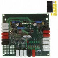
%&.0/453"5*0/�#0"3%�'03�4"���&9
DB62
)551���888�"1&9.*$305&$)�$0.��� ���
�����"1&9��� ���
����������
M I C R O T E C H N O L O G Y
INTRODUCTION
The DB62 is designed to demonstrate the capabilities of
the SA305 as a 3 phase brushless DC motor driver IC. The
PWM inputs to the SA305 are controlled by an on-board
microcontroller. The EVAL49 board is pre-wired for all required
and recommended external components. Please refer to applications note 32 in the Apex catalog for guidance in filter
component selection. The 1µF ceramic capacitors supplied with
the kit are for high frequency bypassing of the VS and VDD
supplies (C1, C11, C4 and C7 on the EVAL49 schematic). Two
additional 100uF bypass capacitors are provided with the kit
for the VS supplies (C2 and C12 on the EVAL49 schematic).
Please refer to applications note 30 for help with power supply
bypassing and other useful information.
PWM CONTROL IN DB62
BLDC motors are electronically commutated based on the
rotor position. The stator windings are energized in a sequence
based upon the combination of three Hall sensor signals which
provide the rotor position. In the DB62 the SA305 input PWM
control is achieved by means of by an on-board Microchip®
PIC 18F2331 microcontroller. The sequence table for commutation (obtained from the motor data sheet) is entered in
the program memory of the microcontroller. Hall sensors A, B
and C are connected to the IC pins of the Input Capture (IC)
module in the PIC18F2331. This module interrupts on every
transition on any of the IC pins. Upon interrupt, the interrupt
service routine reads all the three inputs and loads the correct
sequence for commutation. The following PWM control features
are programmed in the MCU provided with the DB62:
1. User Controlled PWM frequency using external potentiometer (VFREQ in EVAL 49 board). The PWM frequency can
be varied from 4 KHz to 118 KHz.
2. User Controlled PWM duty cycle using external potentiometer (VDUC in EVAL49 board). The voltage set by the
potentiometer will act as a ‘Speed Reference’. The duty
cycle can be varied from 0 % to 98 %.
The Forward/Reverse button is provided to control the
direction of the motor. Depending upon the direction, the corresponding hall sensor commutation sequence is used and the
PWM signals are generated accordingly. The START/STOP
button can be used to run or stop the motor.
As mentioned earlier, the MCU provided with the kit is preprogrammed for all of the features described above. The hall
sensor commutation table that has been used in programming
the MCU is shown in table 1.
Sensor Output
Driver Output
HALLA
HALLB
HALLC
0
0
1
0
1
0
1
ØC (OUTC)
ØB (OUTB)
ØA (OUTA)
X
HI
LO
1
HI
X
LO
1
0
HI
LO
X
1
0
X
LO
HI
1
0
0
LO
X
HI
1
0
1
LO
HI
X
CCW Rotation Facing Lead End
CW Rotation Lead End
0
1
0
LO
HI
X
0
1
1
LO
X
HI
0
0
1
X
LO
HI
1
0
1
HI
LO
X
1
0
0
HI
X
LO
1
1
0
X
HI
LO
Table 1. Commutation Table.
The algorithm for the microcontroller is shown in figure 1. The program for Microchip® PIC 18F2331 is available for download
on www.apexmicrotech.com.
APEX MICROTECHNOLOGY CORPORATION • TELEPHONE (520) 690-8600 • FAX (520) 888-3329 • ORDERS (520) 690-8601 • EMAIL prodlit@apexmicrotech.com
�
�DB62
EVALUATION KIT FOR
SA305EX
*OJUJBMJ[BUJPO
%JTBCMF
/P
4UBSU
:FT
)BMM�4FOTPS
*OQVUT
$IBOHFE
/P
:FT
-PBE�3FWFSTF�5BCMF
#FHJOOJOH�UP�'43
3FWFSTF
'PSXBSE
%JSFDUJPO
-PBE�'PSXBSE�5BCMF
#FHJOOJOH�UP�'43
3FBE�WBMVF�GSPN�5BCMF��
)BMM� PGGTFU
�BOE�MPBE�UP
07%$0/%�SFHJTUFS
4QFFE
3FGFSFODF
$IBOHF
/P
/P
:FT
:FT
3FDBMDVMBUF
18.�%VUZ
$ZDMF
'BVMU
'SFRVFODZ
3FGFSFODF
$IBOHF
3FDBMDVMBUF
18.�'SFRVFODZ
$ZDMF
/P
:FT
Figure 1: Algorithm for Microchip® PIC 18F2331 MCU as implemented for DB62.
APEX MICROTECHNOLOGY CORPORATION • 5980 NORTH SHANNON ROAD • TUCSON, ARIZONA 85741 • USA • APPLICATIONS HOTLINE: 1 (800) 546-2739
�
�EVALUATION KIT FOR
SA305EX
DB62
SPECIAL CONSIDERATIONS
a) 6 schottky diodes D1-D6 (2 for each output provided with
DB62) are recommended for use as external flyback diodes
because of superior reverse recovery characteristics. Please
note that in the DB62, jumpers are needed in order to connect the external schottky diodes (see EVAL49 layout).
b) External RC snubber circuits (R13 and C5, R16 and C8,
R19 and C10 in EVAL49 schematic) can provide noise
immunity especially in high load current scenarios. A 100
V 4.7nF capacitor in series with a 50 ohm 5W resistor
(provided with kit) is recommended for the snubber to be
connected between each output and PGND.
The power dissipated in the snubber components can be
estimated by;
P = V2 • C • FSW
Where
P is the power dissipated
V is the VS supply voltage
C is the snubber capacitor value (15nF)
FSW is the switching frequency.
GROUNDING CONSIDERATIONS
The EVAL49 has three separate ground paths for signal
ground (SGND), power ground (PGND) and digital ground
(DGND). SGND and PGND are the ground paths for the
SA305 while the DGND is for the MCU and related circuitry.
These grounds need to be connected on the board by putting
a jumper between SGND and DGND and another between
PGND and DGND. These jumpers are located in the center
of the board on the right of the SA305. Do not connect the
grounds at any other points to avoid ground loops and unwanted voltage drops.
PARTS LIST
Apex Part #
EVAL49
Description, Vendor
PC Board, Apex
Qty
1
OX7R105KWN
1µF Cap, Novacap
4
MS06
Pin Socket
1
MS11
Socket Strip
(Black) 151-203-RC
Test Point
Mouser
(White) 151-201-RC
(Black) 571-0100
4mm single PCB socket
Deltron
3
ECG-EVQPAC07K
Push Button Switch,
Panasonic
3
3352W-1-102
Potentiometer,
Bourns
2
50SQ100
Schottky Diodes,
International Rectifier
6
140-ESRL100V100
100uF cap,
Xicon
2
MCU-305
PIC18F2331-1/SP-ND
Microchip
1
CFRN60D1001FRE6
1K Ohm Resistor,
(R23,R24.R25)
5% 0.25W
3
RN60D4701FB14
4.7K Ohm Resistor,
(R1, R2, R3, R6)
5% 0.25W
4
CFI-4C1R0J
1 Ohm Resistor,
(R5, R10)
5% 0.25W
2
RN60D2000FB14
200 Ohm Resistor,
(R17, R18, R20,
R21, R22, R26)
5% 0.25W
6
WP63GD
Green LED's,
(D8-D12)
WP631D
Red LED, (D7)
(Optional Components: Refer to SA305U for details)
5
1
Apex Part #
HWRE06
Description, Vendor
Includes the following:
HS32
Heatsink,
Apex
1
3
5
Clip,
Apex
1
Test Point
Mouser
CLAMP05
DIP28 Socket
Mill-Max
1
Thermal Washer,
Apex
1 Box
110-13-328-41-001000
TW12
4mm single PCB socket
Deltron
16
4.7 nF Capacitor,
Kemet
3
(White) 571-0600
C062K472K2X5CA
4mm single PCB socket
Deltron
3
286-51-RC
50 ohm 5W resistor,
Xicon
3
(Red) 571-0500
1 Bag
Qty
APEX MICROTECHNOLOGY CORPORATION • TELEPHONE (520) 690-8600 • FAX (520) 888-3329 • ORDERS (520) 690-8601 • EMAIL prodlit@apexmicrotech.com
�
�DB62
EVALUATION KIT FOR
SA305EX
ASSEMBLY
Before starting the assembly, please review the special considerations section to be able to differentiate between required
and recommended components. The assembly instructions
below cover all the components in the board irrespective of
whether they are required or optional. Use the bread boarding area for any additional circuitry (example: pull-up for hall
sensors) that might be required.
1. Note that each side of the circuit board is identified as either
the “component side” or “bottom side.” The component side
is labeled on the silk screen side of the board. Cut the MS11
strip into strips of 12 and 11. Discard the remaining small
strip of 7. Insert the two strips into the two rows of holes
for the DUT from the component side of the PCB. From
the bottom side, solder all cage jacks to the circuit board
pads. Be sure that the cage jacks are fully seated before
soldering. Be careful that the solder does not flow into the
cage jack. Remove the plastic carrier strips.
2. From the component side, solder a jumper between SGND
and DGND and another between PGND and DGND.
3. From the component side, solder the surface mount capacitors, C1, C4, C7 and C11 and resistors R5 and R10.
4. From the component side, solder jumpers into place for
the following components: R12, R14, R15, R27, R28 and
R29.
5. From the component side, solder pin sockets into place
for the following components: C5, C8, C10, R8, J1A (2 pin
sockets), J1B, J2A, J2B, J3A, J3B and DGND.
6. Study the DIP28 socket and notice the notch on one end.
From the component side, insert the socket, making sure
that the socket has the same orientation as the silk screen
diagram. Solder in the socket from the bottom side.
7. Solder one end of an insulated jumper wire to Pin 11 of the
DIP28 socket, and plug the other end into one of the two
pin sockets at J1A.
8. From the component side, insert the potentiometers VDUC
and VFREQ in the specified orientation and solder from the
bottom side. Carefully bend the potentiometers down to a
horizontal position.
9. From the component side, insert switches SW1 and SW2
and solder from the bottom side.
10. From the component side, insert White Test Points into
TP1, TP2, PWM_HC1, PWM_HB1 and PWM_HA1.
Insert Black Test Points into PWM_LC1, PWM_LB1 and
PWM_LA1. Solder all test points from the bottom side.
11. From the component side, insert the following components:
R1, R2, R3, R6, R7, R11, R17, R20, R26, R22, R21, R18,
R23, R24 and R25, and solder from the bottom side.
12. From the component side, insert LED’s D7, D9, D12, D11,
D10 and D8 and solder from the bottom side.
13. If Hall Effect Sensor pull-up resistors are necessary, install
resistors in bread board to the left of the HALL_A, HALL_B
and HALL_C sockets.
14. Install pin socket in bread board directly under DGND pin
socket.
15. From the component side, insert the 4MM PCB sockets.
Note that there are 4 Black sockets, for SGND, DGND,
PGND and OFF. There are 5 Red sockets, for VPWR,
VDD2, VDD, FAULT and WARNING. The remaining 10
White sockets are for the remaining Input/Output signals.
Solder all sockets from the bottom side.
16. From the component side, insert Schottky diodes D1, D2,
D3, D4, D5 and D6. Solder from the bottom side. Do NOT
trim off excess lead length at this time.
17. If Hall Sensor pull-up resistors are to be used, at this time,
on the bottom side, connect wires from HALL_A, HALL_B,
HALL_C and VDD to the appropriate bread-board sockets
as determined in Step 13.
18. On the bottom side, connect a wire from OFF PCB connector to pin socket directly under DGND pin socket (installed
in Step 14).
19. On the bottom side, connect 16-gauge wire from D4 cathode to AOUT PCB connector. Connect another 16-gauge
wire from D6 cathode to COUT PCB connector. Connect
a third 16-gauge wire from D5 cathode to BOUT PCB
connector. Now, trim off the excess lead length from the
Schottky diodes.
20. From the component side, insert the snubber resistors,
R13, R16 and R19, and solder from the bottom side. Insert
snubber capacitors, C5, C8 and C10 into the previously
installed pin sockets.
21. From the component side, insert the electrolytic capacitors,
C12 and C2, and solder from the bottom side.
22. Install jumper as desired for J3A and/or J3B. Install jumper
from J1A to J1B. If desired, jumper J2A and J2B.
23. Using appropriate hardware, install stand-offs at each
corner hole.
24. Clip the SA305 into the HS32 heat sink with the CLAMP05
clip. Carefully insert the part with the heat sink into the
MS11 sockets. Bolt the heat sink in from the bottom side
of the board using the holes provided on the PCB.
Soft-Start Feature:
A soft start algorithm has been developed so that the
duty cycle at start-up is low and the motor ramps up to the
specified speed reference. The startup duty cycle should be
programmed so that the over current limit of the SA305 is not
exceeded at start-up. The algorithm enables controlling the
rate of acceleration and consequently the maximum current.
When the motor is to be reversed the soft-start algorithm is
once again initiated, causing the motor to gradually accelerate
in the opposite direction. Please refer to application note 45
for details on the soft-start algorithm.
Fault Reset:
The SA305 requires an external reset pulse at the disable
pin to resume normal operation when the part is in a latched
fault condition because of Short-circuit, Over Temperature
(>160°C) or Over-Current (>10 A). In the DB62 board, there
is a provision to reset the part automatically without human
intervention. A jumper needs to be connected between J1A
and P11 of MCU as shown in the schematic. When a fault
occurs, an interrupt is generated which in turn starts generating pulses at P11 to reset the SA305.
APEX MICROTECHNOLOGY CORPORATION • 5980 NORTH SHANNON ROAD • TUCSON, ARIZONA 85741 • USA • APPLICATIONS HOTLINE: 1 (800) 546-2739
�
�DB62
EVALUATION KIT FOR
SA305EX
EVAL49 Schematic
1(/%
4(/%
7183
$�
$$8
'�3
�
51�
3��
3�
$8
3�
���,
3�
3�
$8
$$8
�
�
�
51�
��
7%6$
7'3&2
3�4
18.@-$
%�
065"
%�
065#
%�
%�
%�
065$
3�
�,
%*4"#-&
+�"
3�
3�
��
$�
�V' ���V'
48�
���,
6�
3�
���,
3�
%�
��,
3��
48�
���,
��
��,
+�
+�
+�
��
���
��
��
%�
��
)"--�$
'"6-5
)"--�#
'�3
)"--�"
��
�
%�
���
3��
%��
���
3��
%��
���
3��
%��
���
��
��
��
��
��
%*4"#-&
7183
4(/%
��
��
7%%
��
065"
065#
18.@-#
065$
18.@)$
7183
18.@-$
��
3�4
'"6-5
%�
3��
���
%HOE
*$�
4"���
18.@)#
3��
18.@)"�
3��
��
�
18.@-$�
+�#
��
18.@)$�
18.@-#�
18.@)#�
18.@-"�
'"6-5
+�"
%HOE
%(/%
�
%(/%
7EE
1(/%
$�
�V'
4(/%
�
7%%
18.@-"
��
8"3/*/(
+�#
$�
��
�
#065
���O'
$065
3��
��
��
$��
+�"
3��
�,
���O'
3��
��
*.0/@$
��
��
"065
$�
3��
��
$��
���O'
�
7EE
18.@)"
*.0/@#
18.@-"
��
�
)"--@$
��
��
*.0/@"
5#%
$��
��
/$
5#%
�
��
3��
�
3��
18.@)"
48�
+�#
��
5#%
$��
)"--@$
18.@-#
$�
�V'
0''
)"--@#
7%%�
��
'"6-5
�
��
�
18.@)#
3��
5#%
18.@)$
�
)"--@#
)"--@"
1(/%
3��
�
5#%
1(/%
3��
$��
8"3/*/(
5#%
�
3��
)"--@"
�V'
3��
�,
$��
���V'
3��
�,
0''
*.0/$
*.0/#
*.0/"
APEX MICROTECHNOLOGY CORPORATION • TELEPHONE (520) 690-8600 • FAX (520) 888-3329 • ORDERS (520) 690-8601 • EMAIL prodlit@apexmicrotech.com
�
�DB62
EVALUATION KIT FOR
SA305EX
EVAL49 LAYOUT
501�7*&8
J5
J4
J6
����
����
#0550.�7*&8
This data
sheet has been carefullyCORPORATION
checked and is believed
to beNORTH
reliable, however,
no responsibility
is assumed for
possible inaccuracies
omissions.
All specifications HOTLINE:
are subject to1change
without
notice.
APEX
MICROTECHNOLOGY
• 5980
SHANNON
ROAD • TUCSON,
ARIZONA
85741 •orUSA
• APPLICATIONS
(800)
546-2739
�
DB62U REV B OCTOBER 2006 © 2006 Apex Microtechnology Corp..
�