EK15
EK15
nnoovvaa t i o n FFr roomm
P EK15
r o d u c t IInnSA08
Evaluation Kit for SA08 Pin-Out
INTRODUCTION
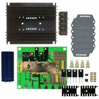
PARTS LIST
This easy-to-use kit provides a platform for the evaluation of
PWM amplifiers using the SA08 pin-out configuration. It can be
used to analyze a multitude of standard or proprietary circuit
configurations, and is flexible enough to do most standard
amplifier test configurations.
The schematic is shown in Figure 3. Note that all of the
components shown on the schematic will probably not be used
for any single circuit. Some components will simply be omitted, while others require installation of a jumper to complete
the signal path.
Only components unique to the EK15 are provided in this
kit. Hardware similar to that shown in Figure 1 must be obtained locally.
Apex Part #
HS18
MS04
EVAL19
60SPG00001
TW05
ZX7R105KTL
OX7R105KWN
TS01
EC01
HS22
CSR03
CSR04
BEFORE YOU GET STARTED
* All Apex Precision Power amplifiers should be handled using
proper ESD precautions.
* Always use the heatsink included in this kit with TW05
washer.
* Always use adequate power supply bypassing.
* Do not change connections while the circuit is powered.
* Initially set all power supplies to the minimum operating
levels allowed in the device data sheet.
* Check for oscillations.
Description
Quantity
Heatsink
1
PC mount Cage Jacks
1 Bag/12 each
PC Board
1
Spacer Grommets
4
Thermal Washer
1 Box/10 each
1µF Cap ST2225B105K501LLXW
2
Novacap
1µF Cap 1825B105K201N,
1
Novacap
Terminal Strip 66505
1
Beau Interconnect
470 µf Cap
1
United Chemi-Con
82DA471M500MG2D
Heatsink
2
Thermolly 6025B
0.010 ohm resistor
2
Caddock MP916-0.010 - 5%
0.020 ohm resistor
2
Caddock MP930-0.020 - 5%
FIGURE 1.
EK15U
http://www.cirrus.com
Copyright © Cirrus Logic, Inc. 2009
(All Rights Reserved)
MAY 20091
APEX − EK15UREVC
�EK15
M I C R O T E C H N O L O G Y
EVAL19 R-C
COMPONENT SIDE
+
PWR
GND
+
B OUT
+Vs
A OUT
Vcc
12
7
Rb
Ra
R1
IC
CVs1
CVs3
4.686
CVcc
CVs2
R2
Vcc SIG
GND
R3
D1
SHDN
SIG
GND
1
6
C3
J1
C2
IC
C1
RAMP/-PWM
OR
FLAG
SIG
GND
R4
SPARE
+PWM
SPARE
5.500
BOTTOM SIDE
6
2
TB1
CIRCUIT DUT SIDE
EVAL19
During assembly refer to Figure 1 and
Figure 2.
1. From the DUT of the PCB insert and
solder the 12 cage jacks. Also solder
the cage jacks from the circuit side
as well, making sure the cage jack
remains flush with the component side
of the PCB.
2. Solder the 3 surface mount ceramic
capacitors to the component side of
the PCB.
3. From the component side of the PCB
insert the terminal strip. Solder from
the circuit side of the PCB. Be sure that
the GND terminal hole in the PCB is
fully filled with solder.
4. Two values of current limiting power
resistors are supplied. Select one
value (see the amplifier data sheet to
learn how to calculate which resistor
will suit your need). Coat the backside
of the power resistor with heat sink
compound (not supplied). Using 4-40
screws and nuts (not supplied) mount
the resistors to the two small heat sinks
supplied. Solder the resistor/heat sink
assembly to the component side of the
PCB.
5. Insert the electrolytic capacitor into
the PCB from the component side and
solder from the circuit side making sure
to fill the mounting holes with solder.
6. From the circuit side, push spacer
grommets into PCB until fully seated.
Grommets will snug when screws are
inserted for heatsink mounting.
7. Apply TW05 thermal washer to the
bottom of the amplifier.
8. Use #14 sleeving to insulate and align
at least 2 opposite pins of the amplifier.
9. Mount amplifier to heatsink using #6
screws and nuts. Torque the part to
the specified 8 to 10 in-lbs (.9 to 1.13
N*M). Do not over torque.
10. Install components as needed. External connections may be soldered
directly or standard banana jacks may
be soldered to the large pads at the
edge of the PCB.
11. Insert amplifier pins into cage jacks
and fasten PCB to heatsink.
FIGURE 2. PCB
TOP SIDE
1
ASSEMBLY
P r o d u c t I n n o v a t i o nF r o m
EK15U
�EK15
P r o d u c t I n n o v a t i o nF r o m
A block diagram of the SA08 is shown in Figure 2 along with
pcb connections of all the commonly used external components.
Your application circuit will not use all of the components. Add
those components required by your circuit. You may have to
jumper some components to make the desired electrical connections. J1 is an optional way to connect the clock circuit. Power
supply bypassing is particularly important and that is why high
quality ceramic chip capacitors are supplied with the kit. In addition, a large electrolytic capacitor is included. This capacitor
was selected expressly for this evaluation kit and may not be
(and likely won't be) suitable for your end application. You will
need to select an electrolytic capacitor based on your analysis
of the capacitor's ripple current, ripple current tolerance, operating temperature, operating voltage, acceptable service life and
acceptable supply ripple. Note that the signal ground and power
ground are separated and tie together only at the ground pin (5).
A breadboarding area is supplied which can accomodate 1 or
2 IC amplifiers and associated components. The large terminal
pads can be used to solder wire connections or bannana jacks.
The schematic of Figure 3 can be used to verify the functionality of your amplifier and help you gain a familiarity with
proper operation. At either A Out or B Out, with respect to
ground, you should observe a square wave approximately 30
V in amplitude with a fixed frequency and duty cycle that varies
from approximately 0 to 100% at a rate of 1 Hz. The current
limit is set to 2 amps.
FIGURE 3. FUNCTIONAL TEST CIRCUIT
50 OHM 25 WATT
DUMMY LOAD
Vcc
Vcc
A OUT
+ Vs
B OUT
CVcc
1µF
FIGURE 3. PCB SCHEMATIC.
A OUT
30V HIGH
AMP
SUPPLY
15V
200 mA
SUPPLY
CVs1-3
Ra
.1 OHM
B OUT
+ Vs
Rb
.1 OHM
R1
5k
R2
5k
CVcc
CVs1-3
12
R1
R2
12
11
I SENSE A
10
8
9
Vcc
A OUT
10V
1000pf
5V
Vcc
910
H
BRIDGE
DRIVER
.01µF
SA08
Vcc
910
50
50k
50
10V
50k
I SENSE B
B OUT
10V
10V
1000pf
7
+ Vs
5V
I SENSE B
.1V
1k
8
9
Vcc
A OUT
I SENSE A
1k
.1V
10
7
B OUT
+ Vs
11
H BRIDGE DRIVER
Ra
10V
.01µF
5V
SA08
TL
56k
f/2 470pF
5V
56k
5V
TL
CLOCK
10V
f/2
470pF
5V
CLK IN
1
CLOCK
CLK IN
2
+ PWM
3
J1
CLK OUT
2
1
CLK OUT
+ PWM
3
C1
J1
4
GND
5
GND ILim/SHDN
FLAG
5
4
C1
.01µF
FLAG
ILim/SHDN
6
C3
.1µF
5K
6
C2
D1
50
C3
R3
+PWM
R4
+PWM
EK15U
D1
RAMP/-PWM
OR
FLAG
SIG
GND
PWR
GND
ILIM/SHDN
RAMP/-PWM
OR
FLAG
SIG
GND
PWR
GND
ILIM/SHDN
1 Hz SDNE WAVE
+3/+7 V AMPLITUDE
VALLEY TO PEAK
3
�EK15
P r o d u c t I n n o v a t i o nF r o m
Contacting Cirrus Logic Support
For all Apex Precision Power product questions and inquiries, call toll free 800-546-2739 in North America.
For inquiries via email, please contact apex.support@cirrus.com.
International customers can also request support by contacting their local Cirrus Logic Sales Representative.
To find the one nearest to you, go to www.cirrus.com
IMPORTANT NOTICE
Cirrus Logic, Inc. and its subsidiaries ("Cirrus") believe that the information contained in this document is accurate and reliable. However, the information is subject
to change without notice and is provided "AS IS" without warranty of any kind (express or implied). Customers are advised to obtain the latest version of relevant
information to verify, before placing orders, that information being relied on is current and complete. All products are sold subject to the terms and conditions of sale
supplied at the time of order acknowledgment, including those pertaining to warranty, indemnification, and limitation of liability. No responsibility is assumed by Cirrus
for the use of this information, including use of this information as the basis for manufacture or sale of any items, or for infringement of patents or other rights of third
parties. This document is the property of Cirrus and by furnishing this information, Cirrus grants no license, express or implied under any patents, mask work rights,
copyrights, trademarks, trade secrets or other intellectual property rights. Cirrus owns the copyrights associated with the information contained herein and gives consent for copies to be made of the information only for use within your organization with respect to Cirrus integrated circuits or other products of Cirrus. This consent
does not extend to other copying such as copying for general distribution, advertising or promotional purposes, or for creating any work for resale.
CERTAIN APPLICATIONS USING SEMICONDUCTOR PRODUCTS MAY INVOLVE POTENTIAL RISKS OF DEATH, PERSONAL INJURY, OR SEVERE PROPERTY OR ENVIRONMENTAL DAMAGE (“CRITICAL APPLICATIONS”). CIRRUS PRODUCTS ARE NOT DESIGNED, AUTHORIZED OR WARRANTED TO BE
SUITABLE FOR USE IN PRODUCTS SURGICALLY IMPLANTED INTO THE BODY, AUTOMOTIVE SAFETY OR SECURITY DEVICES, LIFE SUPPORT PRODUCTS OR OTHER CRITICAL APPLICATIONS. INCLUSION OF CIRRUS PRODUCTS IN SUCH APPLICATIONS IS UNDERSTOOD TO BE FULLY AT THE CUSTOMER’S RISK AND CIRRUS DISCLAIMS AND MAKES NO WARRANTY, EXPRESS, STATUTORY OR IMPLIED, INCLUDING THE IMPLIED WARRANTIES OF
MERCHANTABILITY AND FITNESS FOR PARTICULAR PURPOSE, WITH REGARD TO ANY CIRRUS PRODUCT THAT IS USED IN SUCH A MANNER. IF THE
CUSTOMER OR CUSTOMER’S CUSTOMER USES OR PERMITS THE USE OF CIRRUS PRODUCTS IN CRITICAL APPLICATIONS, CUSTOMER AGREES,
BY SUCH USE, TO FULLY INDEMNIFY CIRRUS, ITS OFFICERS, DIRECTORS, EMPLOYEES, DISTRIBUTORS AND OTHER AGENTS FROM ANY AND ALL
LIABILITY, INCLUDING ATTORNEYS’ FEES AND COSTS, THAT MAY RESULT FROM OR ARISE IN CONNECTION WITH THESE USES.
Cirrus Logic, Cirrus, and the Cirrus Logic logo designs, Apex Precision Power, Apex and the Apex Precision Power logo designs are trademarks of Cirrus Logic, Inc.
All other brand and product names in this document may be trademarks or service marks of their respective owners.
4
EK15U
�