PA03 • PA03A
Power Operational Amplifiers
FEATURES
•
•
•
•
•
•
•
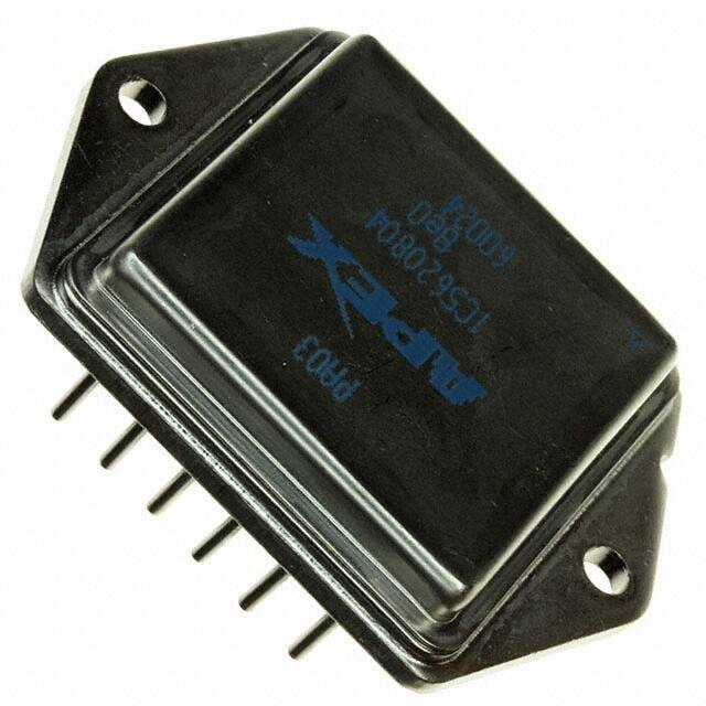
MO-127 Copper Power DIP Package
High Internal Power Dissipation — 500W
High Voltage Operation — ±75V
Very High Current — ±30A
Internal SOA Protection
Output Swings Close to Supply Rails
External Shutdown Control
APPLICATIONS
•
•
•
•
Linear and Rotary Motor Drives
Yoke/Magnetic Field Deflection
Programmable Power Supplies to ±68V
Transducer/Audio to 100W
DESCRIPTION
The super power PA03 advances the state of the art in both brute force power and self-protection against
abnormal operating conditions. Its features start with a copper DIP package developed by Apex Microtechnology to extend power capabilities well beyond those attainable with the familiar TO-3 package. The
increased pin count of the new package provides additional control features, while the superior thermal conductivity of copper allows substantially higher power ratings.
The PA03 incorporates innovative current limiting circuits, limiting internal power dissipation to a curve
approximating the safe operating area of the power transistors. The internal current limit of 35A is supplemented with thermal sensing which reduces the current limit as the substrate temperature rises. Furthermore, a subcircuit monitors actual junction temperatures and with a response time of less than ten
milliseconds reduces the current limit further to keep the junction temperature at 175°C.
The PA03 also features a laser trimmed high performance FET input stage providing superior DC accuracies both initially and over the full temperature range.
Figure 1: Equivalent Schematic
8
11
12
+V
BAL
Q4
Q1
BAL
D1
Q3
Q2
Q6
Q12
Q5
Q18
Q17
–
1
Q20
A
Q20
B
+
2
4
+SHUT
DOWN
Q9
Q7
D2
Q14
+
7
Q16
9
COMP
10
Q22
OUT
Q19
6
–
Q24
3
–SHUT
DOWN
Q29
Q31
D3
Q30
Q32
Q26
Q34
D4
5
–V
www.apexanalog.com
© Apex Microtechnology Inc.
All rights reserved
Feb 2020
PA03U Rev M
�PA03 • PA03A
TYPICAL CONNECTION
Figure 2: Typical Connection
RI
RF
+
+V S
100nF
RBAL
+5V
+V S
+SD
CONTROL
LOGIC
*
PA03
-SD
-V S
V OUT
BAL
CC
BAL
+OUT
-OUT
CC
RL
CC
-V S
100nF
*
*Use 10 μF per Amp of output current
2
PA03U Rev M
�PA03 • PA03A
PINOUT AND DESCRIPTION TABLE
Figure 3: External Connections
Notes: a) Pins 6 & 7 must be connected together.
b) If unused, tie Pins 11 & 12 to +VS
c) IMPORTANT: Observe Mounting precautions. Reverse insertion will destroy unit.
Pin Number
Name
Description
1
2
3
4
5
-IN
+IN
-SD
+SD
-VS
6
-OUT
7
+OUT
8
+VS
9, 10
CC
11, 12
BAL
The inverting input.
The non-inverting input.
The negative shut down pin. See applicable section.
The positive shut down pin. See applicable section.
The negative supply rail.
The negative output. Connect this pin to load and to the feedback resistors. Short to
pin 7.
The positive output. Connect this pin to load and to the feedback resistors. Short to
pin 6.
The positive supply rail.
Compensation capacitor connection. Select value based on Phase Compensation.
See applicable section.
Balance Control pins. Adjusts voltage offset. Short to +VS if unused. See applicable
section.
PA03U Rev M
3
�PA03 • PA03A
SPECIFICATIONS
The power supply voltage for all specifications is the TYP rating unless noted as a test condition.
ABSOLUTE MAXIMUM RATINGS
Parameter
Max
Units
+Vs to -Vs
150
V
Output Current, within SOA
IOUT
Internally Limited
Power Dissipation, internal
PD
500
W
Input Voltage, differential
VIN (Diff)
±25
V
VCM
±VS
V
350
°C
175
°C
-65
+150
°C
-55
+125
°C
±5
±VS
V
Supply Voltage, total
Input Voltage, common mode
Symbol
Min
Temperature, pin solder, 10s max.
Temperature, junction 1
Temperature Range, storage
TJ
Operating Temperature Range, case
TC
Shutdown Voltage, differential
Shutdown Voltage, common mode
V
1. Long term operation at the maximum junction temperature will result in reduced product life. Derate power dissipation
to achieve high MTTF.
CAUTION
4
The internal substrate contains beryllia (BeO). Do not break the seal. If accidentally broken, do
not crush, machine, or subject to temperatures in excess of 850°C to avoid generating toxic
fumes.
PA03U Rev M
�PA03 • PA03A
INPUT
Parameter
Test
Conditions
Offset Voltage, initial
TC = 25°C
Offset Voltage vs. temperature
Full temp range
TC = 25°C
Offset Voltage vs. supply
Offset Voltage vs. power
PA03
Min
Full temp range
Typ
Max
± 0.5
10
Max
±2
± 0.25
± 0.5
mV
30
5
10
µV/°C
µV/V
20
10
µV/W
5
Bias Current vs. supply
TC = 25°C
0.01
Offset Current, initial
TC = 25°C
2.5
Input Impedance, DC
TC = 25°C
10
Input Capacitance
TC = 25°C
6
Common Mode Voltage Range 1
Full temp range
±VS 10V
Common Mode Rejection, DC
Full temp range,
VCM = ±20V
86
Shutdown Current 2
Full temp range
Shutdown Voltage
Units
Typ
*
TC = 25°C
Full temp range,
amp enabled
Full temp range,
amp disabled
Min
8
Bias Current, initial
Shutdown Voltage
PA03A
50
3
10
*
50
1.5
11
pA/V
10
*
100
Ω
*
pF
V
*
dB
*
µA
0.85
3.5
pA
*
*
108
pA
*
*
V
V
1. +VS and –VS denote the positive and negative supply rail respectively. Total VS is measured from +VS to –VS.
2. Rating applies if both shutdown inputs are least 1V inside supply rails. If one of the shutdown inputs is tied to a supply
rail, the current in that pin may increase to 2.4mA.
GAIN
Parameter
Test
Conditions
Full temp range,
full load
T = 25°C, full
Gain Bandwidth Product @ 1 MHz C
load
TC = 25°C, IOUT =
15A, VOUT =
Power Bandwidth
88VPP
Open Loop Gain @10 Hz
Phase Margin
PA03U Rev M
Full temp range,
CC = 1.8nF
PA03
Min
Typ
92
102
PA03A
Max
Max
Units
Min
Typ
*
*
dB
1
*
MHz
30
*
kHz
65
*
°
5
�PA03 • PA03A
OUTPUT
Parameter
Test
Conditions
PA03
Min
Typ
PA03A
Max
Min
Typ
Max
Units
Voltage Swing 1
TC=25°C,
IOUT=30A
± VS - 7
6.2
*
*
V
Voltage Swing 1
Full temp range,
± VS - 5
IOUT = 12A
4.2
*
*
V
Voltage Swing 1
Full temp range,
± VS - 4
IOUT = 146mA
3.5
*
*
V
Current, peak
TC = 25°C
Settling Time to 0.1%
Slew Rate
30
TC = 25°C,
10V step
TC = 25°C,
CC - open
Capacitive Load
Full temp range,
AV = 1
Shutdown Delay
TC = -25°C,
disable
TC = -25°C,
operate
*
A
8
*
µs
8
*
V/µs
2
*
nF
10
*
µs
20
*
µs
1. +VS and –VS denote the positive and negative supply rail respectively. Total VS is measured from +VS to –VS.
POWER SUPPLY
PA03
PA03A
Test
Conditions
Min
Typ
Max
Min
Typ
Max
Voltage
Full temp range
± 15
± 50
± 75
*
*
*
V
Current, quiescent 1
Current, disable mode
TC = 25°C
125
300
*
*
mA
Full temp range
25
40
*
*
mA
Parameter
Units
1. The PA03 must be used with a heatsink or the quiescent power may drive the unit into thermal shutdown.
6
PA03U Rev M
�PA03 • PA03A
THERMAL
Parameter
Resistance, AC junction to case 1
Resistance, DC junction to case
Resistance, junction to ambient
Temperature, junction
Temperature Range, case
Test
Conditions
Full temp range,
F>60 Hz
Full temp range,
F