PA07 • PA07A
FET Input Operational Amplifier
RoHS
COMPLIANT
FEATURES
•
•
•
•
•
Low Bias Current — FET Input
Protected Output Stage — Thermal Shutoff
Excellent Linearity — Class A/B Output
Wide Supply Range — ±12V to ±50V
High Output Current — ±5A Peak
APPLICATIONS
•
•
•
•
•
•
Motor, Valve, and Actuator Control
Magnetic Deflection Circuits up to 4A
Power Transducers up to 100 kHz
Temperature Control up to 180W
Programmable Power Supplies up to 90V
Audio Amplifiers up to 60W RMS
DESCRIPTION
The PA07 is a high voltage, high output current operational amplifier designed to drive resistive, inductive
and capacitive loads. For optimum linearity, especially at low levels, the output stage is biased for class A/B
operation using a thermistor compensated base-emitter voltage multiplier circuit. A thermal shutoff circuit
protects against overheating and minimizes heatsink requirements for abnormal operating conditions. The
safe operating area (SOA) can be observed for all operating conditions by selection of user programmable
current limiting resistors. Both amplifiers are internally compensated for all gain settings. For continuous
operation under load, a heatsink of proper rating is recommended.
This hybrid circuit utilizes thick film (cermet) resistors, ceramic capacitors and semiconductor chips to
maximize reliability, minimize size and give top performance. Ultrasonically bonded aluminum wires provide
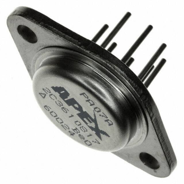
reliable interconnections at all operating temperatures. The 8-pin TO-3 package is hermetically sealed and
electrically isolated. The use of compressible washers and/or improper mounting torque will void the product
warranty. Please see Application Note 1, “General Operating Considerations.”
www.apexanalog.com
© Apex Microtechnology Inc.
All rights reserved
Aug 2015
PA07U Rev U
�PA07 • PA07A
TYPICAL CONNECTION
Figure 1: Typical Connection
Note: Input offset voltage trim optional. RT = 10 kΩ MAX
2
PA07U Rev U
�PA07 • PA07A
PINOUT AND DESCRIPTION TABLE
Figure 2: External Connections
Pin Number
Name
Description
1
OUT
The output. Connect this pin to load and to the feedback resistors.
2
+CL
Connect to the current limit resistor. Output current flows into/out of these pins
through RCL. The output pin and the load are connected to the other side of RCL+.
3
+Vs
The positive supply rail.
4
+IN
The non-inverting input.
5
-IN
The inverting input.
6
-Vs
The negative supply rail.
7
BAL
Balance Control pin. Adjusts voltage offset. See applicable section.
8
-CL
Connect to the current limit resistor. Output current flows into/out of these pins
through RCL. The output pin and the load are connected to the other side of RCL-.
PA07U Rev U
3
�PA07 • PA07A
SPECIFICATIONS
The power supply voltage for all specifications is the TYP rating unless otherwise noted as a test condition.
ABSOLUTE MAXIMUM RATINGS
Parameter
Symbol
Max
Units
+Vs to -Vs
100
V
Output Current, within SOA
IO
5
A
Power Dissipation, internal 1
PD
67
W
VIN (Diff)
±50
V
Vcm
±VS
V
350
°C
200
°C
-65
+150
°C
-55
+125
°C
Supply Voltage, total
Input Voltage, differential
Input Voltage, common mode
Min
Temperature, pin solder, 10s max.
Temperature, junction 1
TJ
Temperature Range, storage
TC
Operating Temperature Range, case
1. Long term operation at the maximum junction temperature will result in reduced product life. Derate internal power dissipation to achieve high MTTF.
CAUTION
The internal substrate contains beryllia (BeO). Do not break the seal. If accidentally broken, do
not crush, machine, or subject to temperatures in excess of 850°C to avoid generating toxic
fumes.
INPUT
Parameter
Test
Conditions
PA07
Min
PA07A
Typ
Max
Min
Typ
Max
Units
Offset Voltage, initial
TC = 25°C
0.5
±2
±0.25
±0.5
mV
Offset Voltage vs. Temperature
Full temp range
10
30
5
10
µV/°C
Offset Voltage vs. Supply
TC = 25°C
8
*
µV/V
Offset Voltage vs. Power
Full temp range
20
10
µV/W
TC = 25°C
5
Bias Current vs. Supply
TC = 25°C
0.01
Offset Current, initial 1
TC = 25°C
2.5
Input Impedance, DC
TC = 25°C
1011
*
Ω
Input Capacitance
TC = 25°C
4
*
pF
Common Mode Voltage Range 2
Full temp range
Common Mode Rejection, DC
Full temp range,
VCM = ±20V
Bias Current, initial
1
±VS–10
50
3
10
*
50
1.5
pA/V
10
*
120
pA
pA
V
*
dB
1. Doubles for every 10°C of temperature increase.
2. +VS and –VS denote the positive and negative supply rail respectively. Total VS is measured from +VS to –VS.
4
PA07U Rev U
�PA07 • PA07A
GAIN
Parameter
Test
Conditions
PA07
Min
Typ
89
95
PA07A
Max
Max
Units
Min
Typ
*
*
dB
Open Loop @ 15 Hz
TC = 25°C,
RL = 15 Ω
Gain Bandwidth Product @ 1 MHz
TC = 25°C,
RL = 15 Ω
1.3
*
MHz
Power Bandwidth
TC = 25°C,
RL = 15 Ω
18
*
kHz
Phase Margin
Full temp range,
RL = 15 Ω
70
*
°
PA07
PA07A
OUTPUT
Parameter
Test
Conditions
Min
Typ
Max
Min
Typ
Max
Units
Voltage Swing 1
Full temp range,
IO = 5A
±VS–5
*
V
Voltage Swing 1
Full temp range,
IO = 2A
±VS–5
*
V
Voltage Swing 1
Full temp range,
IO = 90mA
±VS–5
*
V
Current, peak
TC = 25°C
5
*
A
Settling Time to 0.1%
TC = 25°C, 2V
step
Slew Rate
TC = 25°C
Capacitive Load, unity gain
Full temp range,
1
*
Capacitive Load, gain>4
Full temp range,
SOA
*
1.5
*
µs
5
*
V/µs
nF
1. +VS and –VS denote the positive and negative supply rail respectively. Total VS is measured from +VS to –VS.
POWER SUPPLY
PA07
PA07A
Test
Conditions
Min
Typ
Max
Min
Typ
Max
Voltage
Full temp range
±12
±35
±50
*
*
*
V
Current, quiescent
TC = 25°C
18
30
*
*
mA
Parameter
PA07U Rev U
Units
5
�PA07 • PA07A
THERMAL
Parameter
Test
Conditions
PA07
Min
PA07A
Typ
Max
Min
Typ
Max
Units
Resistance, AC, junction to case 1
F>60 Hz
1.9
2.1
*
*
°C/W
Resistance, DC, junction to case
F