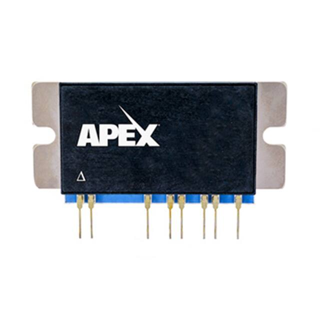
PA194·PA194A
RoHS
Power Operational Amplifier
COMPLIANT
FEATURES
•
•
•
•
High Voltage – 900V
High Speed – 2100V/µs slew rate
Low Noise – 5nV/√Hz @ 10 kHz (typical)
Low Standby Mode Current – 4mA
APPLICATIONS
•
•
•
Test Equipment
Sonar Systems
Industrial Instrumentation
DESCRIPTION
PA194 is a precision power amplifier that can provide a high-voltage, high-speed signal at a very low
noise. It is ideal for applications where high speed analog precision is paramount for the operation of the system. Offered in an 8-pin Power SIP package, the device can handle up to 30W of continuous power dissipation.
Figure 1: Equivalent Schematic
+VS
2*I
Q9
CC
0.5*I
0.5*I
0.5*I
Q6
+IN
Q1A
R1
0.5mA
Q1B
ICL
R8
Q2
R4
OUT
Q3
-IN
Q7
R3
R2
2*I
Q8
+6.2V
ϭ͘ϱDё�
Q4
+
-
I
R6
R5
Q5
MODE
-VS
www.apexanalog.com
6*R6
R7
© Apex Microtechnology Inc.
All rights reserved
Feb 2020
PA194U Rev C
�PA194·PA194A
TYPICAL CONNECTION
Figure 2: Typical Connection
RF
+VS
0.1μF 0.01μF
C1
RIN
-
CC
+VS
+
AC
C2
IN
D1
CC
PA194
D2
MODE
+
-VS
2
-VS
ILIM
OUT
VOUT
RLIM
S1
FOR STANDBY MODE
0.1μF
0.01μF
C1
C2
PA194U Rev C
�PA194·PA194A
PINOUT AND DESCRIPTION TABLE
Figure 3: External Connections
1
2
7
-IN
+IN
CC
9
10
MODE -V S
12
13
ILIM OUT
15
+V S
Pin Number
Name
Description
1
2
7
9
10
-IN
+IN
CC
MODE
-VS
12
ILIM
13
15
3, 4, 5, 6, 8, 11,
14
OUT
+VS
Inverting input
Non-inverting input
Compensation capacitor connection to ground
MODE = -VS -> Standby Mode, MODE = OPEN -> Normal Operation.
Negative supply rail
Connect to the current limit resistor. Output current flows into/out of this pin
through RLIM. The output pin and the load are connected to the other side of RLIM.
Output. Connect this pin to load and to the feedback resistors.
Positive supply rail
NC
No Connection/No Pin
PA194U Rev C
3
�PA194·PA194A
SPECIFICATIONS
Unless otherwise noted: TC = 25°C, CC = open, AV = -100 V/V, MODE is open. DC input specifications are
± value given. Power supply voltage is + 300V.
ABSOLUTE MAXIMUM RATINGS
Parameter
Supply Voltage, total
Output Current, peak, within SOA
Power Dissipation, internal, DC
Input Voltage, differential
Temperature, pin solder, 10s max.
Temperature, junction 1
Temperature Range, storage
Operating Temperature Range, case
Symbol
+Vs to -Vs
IOUT
PD
VIN (Diff)
TJ
TC
Min
-20
-55
-40
Max
Units
900
200
30
20
260
150
+125
+85
V
mA
W
V
°C
°C
°C
°C
1. Long term operation at the maximum junction temperature will result in reduced product life. Derate internal power
dissipation to achieve high MTTF.
4
PA194U Rev C
�PA194·PA194A
INPUT
Parameter
Test
Conditions
PA194
Min
Offset Voltage, initial
Offset Voltage vs. Temperature
0°C to 85°C
Typ
Max
PA194A
Min
Typ
Max
0.5
5
*
10
Offset Voltage vs. Time
75
Bias Current, initial
1
15
Bias Current vs. Supply
4
Offset Current, initial
8
Input Resistance, DC
10
Input Capacitance
VS= ±450V
-VS+40
Common Mode Rejection, DC
VCM = ±90V
92
Noise Density
*
15
*
400
10 kHz BW,
RIN = 100 Ω
RIN = 100 Ω,
F = 10 kHz
*
11
+VS–40
4
µV/V
µV/kh
*
pA
pA/V
*
pA
*
Ω
*
pF
*
*
*
460
*
*
200
mV
µV/°C
*
25
Common Mode Voltage Range2
Integrated Noise
*
25
Offset Voltage vs. Supply
*
Units
V
dB
*
*
nV RMS
nV/Hz
1. Doubles for every 10°C of case temperature increase.
2. Although supply voltages can range up to ±450V the input pins cannot swing over this range. The input pins must be at
least 40 V from either supply rail but not more than 450V from negative supply rail, -VS. However, the inputs can be
860V from the positive supply rail, +VS.
PA194U Rev C
5
�PA194·PA194A
GAIN
Parameter
Test
Conditions
PA194
Min
Typ
96
110
Open Loop Gain @ 15 Hz
RL = 5 kΩ
Gain Bandwidth Product @ 1
MHz
RL = 5 kΩ
140
Power Bandwidth
RL = 5 kΩ
800
Phase Margin, AV=100 V/V
Full temp
range
30
PA194A
Max
Min
*
Typ
Max
*
Units
dB
*
MHz
*
kHz
*
°
OUTPUT
Parameter
Voltage Swing1
Voltage Swing
1
Test
Conditions
PA194
Min
Typ
Max
PA194A
Min
Typ
Max
Units
IOUT =70mA,DC
+VS-12 +VS-25
*
*
V
IOUT = 70mA,DC
-VS+22 -VS+25
*
*
V
Current, continuous, DC
*
100
Slew Rate, AV = -100 V/V 2
2100
Settling Time to 0.1%
2V step
Output Resistance
No load, DC,
Closed loop
1
100
1800
mA
*
V/µs
*
µs
*
Ω
1. Please refer to Output Voltage Drop vs Frequency Plot
2. Ground heat tab for higher slew rate
6
PA194U Rev C
�PA194·PA194A
POWER SUPPLY
Parameter
Test
Conditions
PA194
Min
Voltage
±50
Current, quiescent (normal
operation)
20
Current, quiescent (standby
mode)
Typ
25
PA194A
Max
Min
±450
*
30
Max
*
*
*
Units
V
*
mA
*
4
Mode = -VS
Typ
mA
THERMAL
PA194
PA194A
Parameter
Test
Conditions
Resistance, AC, junction to case1
Full temp
range, F≥60Hz
3
*
°C/W
Resistance, DC, junction to case
Full temp
range, F