PA343
PA343
PA343
High Voltage Power Operational Amplifier
DESCRIPTION
FEATURES
The PA343 is a dual high voltage monolithic MOSFET
operational amplifier achieving performance features
previously found only in hybrid designs while increasing reliability. This approach provides a cost-effective
solution to applications where multiple amplifiers are
required. Inputs are protected from excessive common
mode and differential mode voltages. The safe operating area (SOA) has no secondary breakdown limitations and can be observed with all type loads by choosing an appropriate current limiting resistor. External
compensation provides the user flexibility in choosing
optimum gain and bandwidth for the application.
♦ RoHS COMPLIANT
♦ SURFACE MOUNT PACKAGE
♦ MONOLITHIC MOS TECHNOLOGY
♦ LOW COST
♦ HIGH VOLTAGE OPERATION – 350V
♦ LOW QUIESCENT CURRENT TYP. – 2.2mA
♦ NO SECOND BREAKDOWN
♦ HIGH OUTPUT CURRENT – 120 mA PEAK
APPLICATIONS
♦ TELEPHONE RING GENERATOR
♦ PIEZO ELECTRIC POSITIONING
♦ ELECTROSTATIC TRANSDUCER &
DEFLECTION
♦ DEFORMABLE MIRROR FOCUSING
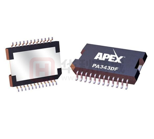
The PA343DF is packaged in a 24 pin PSOP (JEDEC
MO-166) package. The heatslug of the PA343DF
package is isolated in excess of full supply voltage.
FIGURE 1: Equivalent Schematic (one of 2 Amplifiers)
+VS
Q1
Q2
Q3
C C1
Q4
CC2
+IN
-IN
Q5
Q7
Q8
Q9
D4
D1
D2
ILIM
Q6
Q11
Q10
OUT
Q13
D3
Q12
Q14
Q15
D5
-VS
Copyright © Apex Microtechnology, Inc. 2014
www.apexanalog.com
PA343U
(All Rights Reserved)
JAN 2014
1
PA343U REV D
�PA343
FIGURE 2. External Connections.
*
1
+Vsa
NC
-Vsa
24
NC
ILa
COMPa
RCL
+INa
+
A
COMPa
CC
*
NC
-INa
-
OUTa
NC
OUTb
NC
-INb
COMPb
-
B
+INb
RCL
COMPb
+
ILb
CC
NC
*
+Vsb
-Vsb
*
For CC values, see graph on page 4.
Note: CC must be rated for full supply voltage.
* Supply bypassing required. See general Operating Considerations.
24-pin PSOP
PACKAGE STYLE DF
TYPICAL APPLICATION
A single PA343 amplifier operates as a bridge driver for a piezo transducer providing a low cost 660 volt total drive
capability. The RN CN network serves to raise the apparent gain of A2 at high frequencies. If RN is set equal to R the
amplifiers can be compensated identically and will have matching bandwidths. See application note 20 for more
details.
R
VIN
20R
20R
20R
+175
+175
10pF
A
PA343
R CL
47
–175
10pF
R CL
B
PA343
PIEZO
TRANSDUCER 47
RN
CN
–175
FIGURE 3. Low Cost 660v p-p Piezo Drive
2
PA343U
�PA343
1. CHARACTERISTICS AND SPECIFICATIONS
ABSOLUTE MAXIMUM RATINGS
Parameter
Symbol
Min
Max
Units
350
V
OUTPUT CURRENT, continuous within SOA
60
mA
OUTPUT CURRENT, peak
120
mA
POWER DISSIPATION, continuous @ TC = 25°C (Note 7)
12
W
SUPPLY VOLTAGE, +VS to -VS
INPUT VOLTAGE, differential
-16
+16
V
INPUT VOLTAGE, common mode
-VS
+VS
V
220
°C
TEMPERATURE, pin solder - 10 sec
TEMPERATURE, junction (Note 2)
150
°C
TEMPERATURE, storage
-65
150
°C
TEMPERATURE RANGE, powered (case)
-40
125
°C
SPECIFICATIONS (PER AMPLIFIER)
Parameter
Test Conditions (Note 1)
Min
Typ
Max
Units
OFFSET VOLTAGE, initial
12
40
mV
OFFSET VOLTAGE, vs. temperature
25°C to 85°C
(Note 3)
17
250
µV/°C
OFFSET VOLTAGE, vs. temperature
-25°C to 25°C
(Note 3)
18
500
µV/°C
OFFSET VOLTAGE, vs. supply
4.5
OFFSET VOLTAGE, vs. time
80
BIAS CURRENT, initial
50
BIAS CURRENT, vs. supply
2
INPUT
OFFSET CURRENT, initial
50
INPUT IMPEDANCE, DC
INPUT CAPACITANCE
µV/V
µV/kh
200
pA
pA/V
200
pA
1011
Ω
3
pF
COMMON MODE, voltage range
+VS - 12
V
COMMON MODE, voltage range
-VS + 12
V
COMMON MODE REJECTION, DC
VCM = ±90VDC
NOISE, broad band
10kHz BW, RS = 1KΩ
84
115
dB
337
µV RMS
GAIN
OPEN LOOP at 15Hz
RL = 5KΩ
103
dB
GAIN BANDWIDTH PRODUCT
@1MHz
10
MHz
POWER BANDWIDTH
280V p-p
35
kHz
PA343U
90
3
�PA343
Parameter
Test Conditions (Note 1)
Min
Typ
±VS - 12
±VS - 10
Max
Units
OUTPUT
VOLTAGE SWING
IO = 40mA
V
CURRENT, peak (Note 3)
120
mA
CURRENT, continuous
60
mA
SETTLING TIME to 0.1%
10V step, A V = -10
2
µs
SLEW RATE
CC = 4.7pF
32
V/µS
RESISTANCE, 10mA (Note 4) RCL = 0Ω
91
Ω
RESISTANCE, 40mA (Note 4) RCL = 0Ω
65
Ω
POWER SUPPLY
VOLTAGE
±10
CURRENT, quiescent (Note 7)
±150
±175
V
2.2
2.5
mA
THERMAL
RESISTANCE, junction to case
AC, single amplifier
F > 60Hz
6
7
°C/W
DC, single amplifier
F < 60Hz
9
11
°C/W
AC, both amplifier (Note 5)
3.3
4.0
°C/W
DC, both amplifier (Note 5)
5.0
6.0
°C/W
RESISTANCE, junction to air
Full temperature range
(Note 6)
25
TEMPERATURE RANGE, case
Meets full range specifications
-25
°C/W
+85
°C
NOTES:
1. Unless otherwise noted TC = 25°C, CC = 6.8pF. DC input specifications are ± value given. Power supply voltage is typical rating.
2. Long term operation at the maximum junction temperature will result in reduced product life. Derate
internal power dissipation to achieve high MTTF. For guidance, refer to heatsink data sheet.
3. Guaranteed but not tested.
4. The selected value of RCL must be added to the values given for total output resistance.
5. Rating applies when power dissipation is equal in the two amplifiers.
6. Rating applies with solder connection of heatslug to a minimum 1in2 foil area of the printed circuit
board.
7. Specifications are for individual amplifiers in this device, unless otherwise noted.
CAUTION
The PA343 is constructed from MOSFET transistors. ESD handling procedures must be observed.
4
PA343U
�PA343
Both Amplifiers
Single Amplifier
20
0.80
0.75
15
VBE+
0.70
T = TC
0.65
5
0
T = TA
0.60
T = TA
0.55
0
20
40
60
80
TEMPERATURE, T (C)
0.50
-40 -20
100
PHASE, Φ (°)
60
2.2pF
6.8pF
40
2.2pF
6.8pF
-140
-150
68pF
15pF
-160
0
-170
-20
10
10
-110
-130
15pF
20
0.75pF
-120
100 1K 10K 100K 1M 10M
FREQUENCY, F (Hz)
-180
10K
100K
1M
FREQUENCY, F (Hz)
HARMONIC DISTORTION
10M
SLEW RATE
A V = 20
C C = 15pF
R L = 2K
1K
10K
FREQUENCY, F (Hz)
80
60
40
20
0
10
100
1K
10K
FREQUENCY, F (Hz)
100K
RISE
5 15 25 35 45 55 65 75 85
COMPENSATION CAPACITANCE, CC (pF)
POWER SUPPLY REJECTION
COMMON MODE REJECTION
100
10
0
100K
120
FALL
20
100
80
70
25°C
55°C
1
NEGATIVE
60
15pF
33pF
68pF
10
10K
100K
FREQUENCY, F (Hz)
1M
QUIESCENT CURRENT
102
)
5°C
12
100
I Q(
°C)
5
I Q(2
C)
40°
98
I Q(-
96
20 60 100 140 180 220 260 300 340
TOTAL SUPPLY VOLTAGE, (V)
OUTPUT VOLTAGE SWING
VDROP+@85°C
20
VDROP-@85°C
15
VDROP-@27°C
10
40
10
0
PA343U
POWER RESPONSE
100
5
100K
10
2.2pF
6.8pF
50
100
1K
10K
FREQUENCY, F (Hz)
1
GAIN
25
POSITIVE
90
10
30
VDROP FROM VS, (V)
0.01
SLEW RATE, (V/us)
0.1 180V
P-P
0.001
100
COMMON MODE REJECTION, CMR (dB)
30VP-P
60VP-P
POWER SUPPLY REJECTION, PSR (dB)
DISTORTION, (%)
30
1
125°C
85°C
1000
68pF
-100
0.75pF
GAIN AND COMPENSATION
0.1
0.1
0 20 40 60 80 100 120
TEMPERATURE (°C)
PHASE RESPONSE
-80
-90
100
80
VBE-
OUTPUT VOLTAGE, (VOUT) (P-P)
10
SMALL SIGNAL RESPONSE
OPEN LOOP GAIN, A (dB)
100
COMPENSATION, pF
T = TC
VBE for ILIMIT
0.85
NORMALIZED QUIESCENT CURRENT (%)
POWER DERATING
25
VBE (V)
INTERNAL POWER DISSIPATION, P(W)
2. TYPICAL PERFORMANCE GRAPHS
VDROP+@27°C
0
20 40 60 80 100 120
OUTPUT CURRENT, IO (mA)
5
�PA343
3.
APPLICATION INFORMATION
3.1
PHASE COMPENSATION
3.2
OTHER STABILITY CONCERNS
Please read Application Note 1 "General Operating Considerations" which covers stability, power supplies, heat
sinking, mounting, current limit, SOA interpretation, and specification interpretation. Visit www.apexanalog.com
for design tools that help automate tasks such as calculations for stability, internal power dissipation, current limit,
heat sink selection, Apex Microtechnology's complete Application Notes library, Technical Seminar Workbook and
Evaluation Kits.
Open loop gain and phase shift both increase with increasing temperature. The PHASE COMPENSATION typical
graph shows closed loop gain and phase compensation capacitor value relationships for four case temperatures.
The curves are based on achieving a phase margin of 50°. Calculate the highest case temperature for the application (maximum ambient temperature and highest internal power dissipation) before choosing the compensation.
Keep in mind that when working with small values of compensation, parasitics may play a large role in performance
of the finished circuit. The compensation capacitor must be rated for at least the total voltage applied to the amplifier
and should be a temperature stable type such as NPO or COG.
There are two important concepts about closed loop gain when choosing compensation. They stem from the fact
that while "gain" is the most commonly used term, β (the feedback factor) is really what counts when designing for
stability.
1. Gain must be calculated as a non-inverting circuit (equal input and feedback resistors can provide a signal gain
of -1, but for calculating offset errors, noise, and stability, this is a gain of 2).
2. Including a feedback capacitor changes the feedback factor or gain of the circuit. Consider Rin=4.7k, Rf=47k
for a gain of 11. Compensation of 4.7 to 6.8pF would be reasonable. Adding 33pF parallel to the 47k rolls off the
circuit at 103kHz, and at 2MHz has reduced gain from 11 to roughly 1.5 and the circuit is likely to oscillate.
As a general rule the DC summing junction impedance (parallel combination of the feedback resistor and all input
resistors) should be limited to 5k ohms or less. The amplifier input capacitance of about 6pF, plus capacitance of
connecting traces or wires and (if used) a socket will cause undesirable circuit performance and even oscillation if
these resistances are too high. In circuits requiring high resistances, measure or estimate the total sum point capacitance, multiply by Rin/Rf, and parallel Rf with this value. Capacitors included for this purpose are usually in the
single digit pF range. This technique results in equal feedback factor calculations for AC and DC cases. It does not
produce a roll off, but merely keeps β constant over a wide frequency range. Paragraph 6 of Application Note 19
details suitable stability tests for the finished circuit.
3.3
CURRENT LIMIT
For proper operation, the current limiting resistor, RCL, must be connected as shown in Figure 3, “External Connections”. The current limit can be predicted as follows:
ILIMIT =
VBE
RCL
The “VBE for ILIMIT” performance graph is used to find VBE. On this graph, the VBE+ and VBE− curves show the voltages
across the current limiting resistor at which current limiting is turned on. The VBE+ curve shows these turn-on voltages when the amplifier is sourcing current, and the VBE− curve shows these voltages when the amplifier is sinking
current.
The current limit can be thought of as a ceiling or limit for safe operation. For continuous operation it is any value
between the desired load current and 60 mA (as long as the curves on the SOA graph are not exceeded, please
6
PA343U
�PA343
refer to section 3.4 for information on the SOA graph). As an example, suppose the desired load current for the application is 20 mA. In this case we may set a current limit of 30 mA. Starting with the smaller VBE− of 0.6 we have:
RCL =
0.6
= 20Ω
1.03
For the larger VBE+ this RCL resistor will allow for a maximum current of:
ILIMIT =
0.7
= 35mA
20
This value is still acceptable because it is less than 60 mA. For the case of continuous load currents, check that the
current limit does not exceed 60 mA.
The VBE values used above are approximate and can vary with process. To allow for this possibility the user can
reduce the VBE = 0.6 value by 20%. This results in a RCL value of 16 Ω. Using this same RCL value and allowing for
a 20% increase in the other VBE , the current limit maximum is 52 mA.
The absolute minimum value of the current limiting resistor is bounded by the largest current and the largest
VBE in the application. The largest VBE is determined by the coldest temperature in the application. In general the
largest VBE is VBE+ = 0.78, which occurs at T = − 40°C. The largest allowed current occurs in pulsed applications
where, from the SOA graph, we can see current pulses of 120 mA. This gives us an absolute minimum RCL value of
0.78/0.12 = 6.5Ω.
3.4
SAFE OPERATING AREA
1. Voltage withstand capability of the transistors.
2. Current handling capability of the die metalization.
3. Temperature of the output MOSFETS.
These limitations can be seen in the SOA (see Safe Operating
Area graphs). Note that each pulse capability line shows a constant power level (unlike second breakdown limitations where
power varies with voltage stress). These lines are shown for a
case temperature of 25°C and correspond to thermal resistances
of 5.2°C/W for the PA343DF. Pulse stress levels for other case
temperatures can be calculated in the same manner as DC power levels at different temperatures. The output stage is protected
against transient flyback by the parasitic diodes of the output
stage MOSFET structure. However, for protection against sustained high energy flyback external fast-recovery diodes must be
used.
OUTPUT CURRENT FROM +VS or -VS, (mA)
The MOSFET output stage of the PA343 is not limited by second FIGURE 4. Safe Operating Area
breakdown considerations as in bipolar output stages. However
PA343 SOA
there are still three distinct limitations:
200
120
100
50
40
30
20
10
5
4
3
20
30
0m
S
0m
S
DC
,T
C
DC
DC
,T
C
=
=
85
°C
12
5
°C
PULSE CURVES @
10% DUTY CYCLE MAX.
2
10
20 30 50
100
200 300 500
SUPPLY TO OUTPUT DIFFERENTIAL, V S- V O (V)
3.5 HEATSINKING
The PA343DF package has a large exposed integrated copper heatslug to which the monolithic amplifier is directly
attached. The solder connection of the heatslug to a minimum of 1 square inch foil area on the printed circuit board
will result in thermal performance of 25°C/W junction to air rating of the PA343DF. Solder connection to an area of 1
to 2 square inches is recommended. This may be adequate heatsinking but the large number of variables involved
suggest temperature measurements be made on the top of the package. Do not allow the temperature to exceed
85°C.
PA343U
7
�PA343
3.6
OVERVOLTAGE PROTECTION
Although the PA343 can withstand differential input voltages up to 16V, FIGURE 5. Overvoltage Protection
in some applications additional external protection may be needed. Dif+Vs Z1
ferential inputs exceeding 16V will be clipped by the protection circuitry.
However, if more than a few milliamps of current is available from the
overload source, the protection circuitry could be destroyed. For differen+Vs
-IN
tial sources above 16V, adding series resistance limiting input current to
1mA will prevent damage. Alternatively, 1N4148 signal diodes connected
OUT
Q1
anti-parallel across the input pins is usually sufficient. In more demanding
Q2
applications where bias current is important, diode connected JFETs such
as 2N4416 will be required. See Q1 and Q2 in Figure 5. In either case the +IN
-Vs
differential input voltage will be clamped to 0.7V. This is sufficient overdrive
to produce the maximum power bandwidth.
In the case of inverting circuits where the +IN pin is grounded, the diodes
Z2
-Vs
mentioned above will also afford protection from excessive common mode
voltage. In the case of non-inverting circuits, clamp diodes from each input to each supply will provide protection.
Note that these diodes will have substantial reverse bias voltage under normal operation and diode leakage will
produce errors.
Some applications will also need over-voltage protection devices connected to the power supply rails. Unidirectional
zener diode transient suppressors are recommended. The zeners clamp transients to voltages within the power
supply rating and also clamp power supply reversals to ground. Whether the zeners are used or not the system
power supply should be evaluated for transient performance including power-on overshoot and power-off polarity
reversals as well as line regulation. See Z1 and Z2 in Figure 5.
NEED TECHNICAL HELP? CONTACT APEX SUPPORT!
For all Apex Microtechnology product questions and inquiries, call toll free 800-546-2739 in North America.
For inquiries via email, please contact apex.support@apexanalog.com.
International customers can also request support by contacting their local Apex Microtechnology Sales Representative.
To find the one nearest to you, go to www.apexanalog.com
IMPORTANT NOTICE
Apex Microtechnology, Inc. has made every effort to insure the accuracy of the content contained in this document. However, the information is subject to change
without notice and is provided "AS IS" without warranty of any kind (expressed or implied). Apex Microtechnology reserves the right to make changes without further
notice to any specifications or products mentioned herein to improve reliability. This document is the property of Apex Microtechnology and by furnishing this information, Apex Microtechnology grants no license, expressed or implied under any patents, mask work rights, copyrights, trademarks, trade secrets or other intellectual
property rights. Apex Microtechnology owns the copyrights associated with the information contained herein and gives consent for copies to be made of the information only for use within your organization with respect to Apex Microtechnology integrated circuits or other products of Apex Microtechnology. This consent does not
extend to other copying such as copying for general distribution, advertising or promotional purposes, or for creating any work for resale.
APEX MICROTECHNOLOGY PRODUCTS ARE NOT DESIGNED, AUTHORIZED OR WARRANTED TO BE SUITABLE FOR USE IN PRODUCTS USED FOR
LIFE SUPPORT, AUTOMOTIVE SAFETY, SECURITY DEVICES, OR OTHER CRITICAL APPLICATIONS. PRODUCTS IN SUCH APPLICATIONS ARE UNDERSTOOD TO BE FULLY AT THE CUSTOMER OR THE CUSTOMER’S RISK.
Apex Microtechnology, Apex and Apex Precision Power are trademarks of Apex Microtechnolgy, Inc. All other corporate names noted herein may be trademarks
of their respective holders.
Copyright © Apex Microtechnology, Inc. 2014
www.apexanalog.com
8
(All Rights Reserved)
JAN 2014
PA343U
PA343U REV D
�