PA84 • PA84A
• PA84S
PA84 • PA84A
• PA84S
PA84, PA84A, PA84S
Power Operational Amplifiers
FEATURES
• HIGH SLEW RATE — 200V/µs
• FAST SETTLING TIME — .1% in 1µs (PA84S)
• FULLY PROTECTED INPUT — Up to ±150v
• LOW BIAS CURRENT, LOW NOISE — FET Input
• WIDE SUPPLY RANGE — ±15V to ±150V
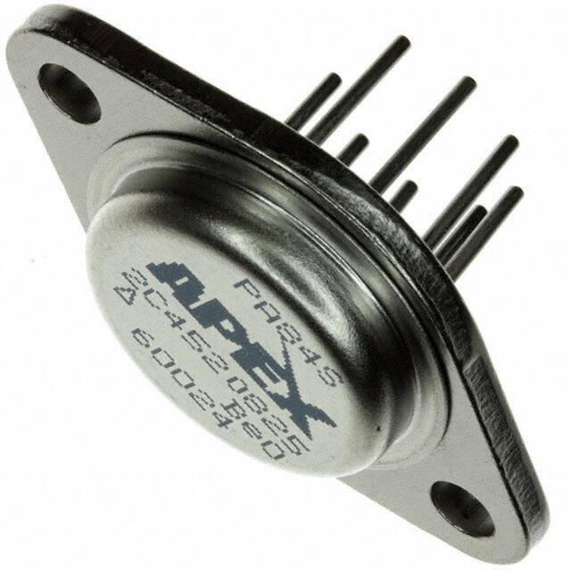
8-PIN TO-3
PACKAGE STYLE CE
APPLICATIONS
• HIGH VOLTAGE INSTRUMENTATION
• ELECTROSTATIC TRANSDUCERS & DEFLECTION
• PROGRAMMABLE POWER SUPPLIES UP TO 290V
• ANALOG SIMULATORS
100K 50K
+150V
DESCRIPTION
The PA84 is a high voltage operational amplifier designed
for output voltage swings up to ±145V with a dual supply or
290V with a single supply. Two versions are available. The
new PA84S, fast settling amplifier can absorb differential input
overvoltages up to ±50V while the established PA84 and PA84A
can handle differential input overvoltages of up to ±300V. Both
versions are protected against common mode transients and
overvoltages up to the supply rails. High accuracy is achieved
with a cascode input circuit configuration. All internal biasing
is referenced to a zener diode fed by a FET constant current
source. As a result, the PA84 features an unprecedented supply range and excellent supply rejection. The output stage is
biased-on for linear operation. External phase compensation
allows for user flexibility in obtaining the maximum slew rate.
Fixed current limits protect these amplifiers against shorts
to common at supply voltages up to 150V. For operation into
inductive loads, two external flyback pulse protection diodes
are recommended. However, a heatsink may be necessary to
maintain the proper case temperature under normal operating
conditions.
This hybrid integrated circuit utilizes a beryllia (BeO) substrate, thick film resistors, ceramic capacitors and semiconductor chips to maximize reliability, minimize size and give top
performance. Ultrasonically bonded aluminum wires provide
reliable interconnections at all operating temperatures. The
8-pin TO-3 package is hermetically sealed and electrically
isolated. The use of compressible thermal isolation washers
and/or improper mounting torque will void the product warranty.
Please see “General Operating Considerations”.
EXTERNAL CONNECTION
-VS
COMP
RC
7
8
5 –IN
TOP VIEW
4
OUT
1
+VS
2
3
BAL
www.apexanalog.com
PA84U
BAL
GAIN
CC
RC
1
10
100
1000
10nF
500pF
50pF
none
200Ω
2KΩ
20KΩ
none
NOTES:
1. Phase Compensation required
for safe operation.
2. Input offset trimpot optional.
Recommended value 100KΩ.
10K
PA84
••••••
••••••
••••••
–150V
TYPICAL APPLICATION
The PA84 is ideally suited to driving ink jet control units (often
a piezo electric device) which require precise pulse shape
control to deposit crisp clear date or lot code information on
product containers. The external compensation network has
been optimized to match the gain setting of the circuit and the
complex impedance of the ink jet control unit. The combination
of speed and high voltage capabilities of the PA84 form ink
droplets of uniform volume at high production rates to enhance
the value of the printer.
EQUIVALENT SCHEMATIC
4
2
C1
D1
3
Q3
Q2
Q1
Q4
Q5
Q6
8
Q8
C5
PHASE COMPENSATION
+IN
390pF
10V
INK JET
CONTROL
5
6
CC
DAC
4.7K
6
*
C4
Q7
Q10
Q11
Q12B
1
Q12A
*
Q13 *
Q14 *
*
C6
7
Q9
Q16
Q17
Q15
*
D2
*Not included in PA84S.
Copyright © Apex Microtechnology, Inc. 2014
(All Rights Reserved)
OCT 2015
1
PA84U REVV
�PA84 • PA84A • PA84S
ABSOLUTE MAXIMUM RATINGS
SPECIFICATIONS
SUPPLY VOLTAGE, +VS to –VS
OUTPUT CURRENT, within SOA
POWER DISSIPATION, internal at TC = 25°C2
INPUT VOLTAGE, differential PA84/PA84A1
INPUT VOLTAGE, differential PA84S
INPUT VOLTAGE, common mode1
TEMPERATURE, pins for 10s max (solder)
TEMPERATURE, junction2
TEMPERATURE RANGE, storage
OPERATING TEMPERATURE RANGE, case
MIN
PA84/PA84S PA84A
TYP
MAX MIN TYP MAX UNITS
PARAMETER
TEST CONDITIONS 3
INPUT
OFFSET VOLTAGE, initial
OFFSET VOLTAGE, vs. temperature
OFFSET VOLTAGE, vs. supply
OFFSET VOLTAGE, vs. time
BIAS CURRENT, initial4
BIAS CURRENT, vs. supply
OFFSET CURRENT, initial4
OFFSET CURRENT, vs. supply
INPUT IMPEDANCE, DC
INPUT CAPACITANCE
COMMON MODE VOLTAGE RANGE5
COMMON MODE REJECTION, DC
TC = 25°C
TC = –25° to +85°C
TC = 25°C
TC = 25°C
TC = 25°C
TC = 25°C
TC = 25°C
TC = 25°C
TC = 25°C
TC = –25° to +85°C
TC = –25° to +85°C
TC = –25° to +85°C
GAIN
OPEN LOOP GAIN at 10Hz
OPEN LOOP GAIN at 10Hz.
GAIN BANDWIDTH PRODUCT@ 1MHz
POWER BANDWIDTH, high gain
POWER BANDWIDTH, low gain
TC = 25°C, RL = ∞
TC = 25°C, RL = 3.5KΩ
TC = 25°C, RL = 3.5KΩ, RC = 20KΩ
TC = 25°C, RL = 3.5KΩ, RC = 20KΩ
TC = 25°C, RL = 3.5KΩ, RC = 20KΩ
OUTPUT
VOLTAGE SWING5
VOLTAGE SWING5
CURRENT, peak
CURRENT, short circuit
SLEW RATE, high gain
SLEW RATE, low gain
SETTLING TIME .01% at gain = 100
SETTLING TIME .1% at gain = 100
SETTLING TIME .01% at gain = 100
SETTLING TIME .1% at gain = 100
TC = 25°C, IO = ±40mA
±VS–7
TC = –25° to +85°C, IO = ±15mA
±VS–5
TC = 25°C
40
TC = 25°C
TC = 25°C, RL = 3.5KΩ, RC = 20KΩ
TC = 25°C, RL = 3.5KΩ, RC = 2KΩ
TC = 25°C, RL = 3.5KΩ
PA84S
RC = 20KΩ, VIN = 2V step ONLY
TC = 25°C, RL = 3.5KΩ
PA84/84A
RC = 20KΩ, VIN = 2V step
POWER SUPPLY
VOLTAGE
CURRENT, quiescent
TC = –55°C to +125°C
TC = 25°C
THERMAL
RESISTANCE, AC, junction to case6
RESISTANCE, DC, junction to case
RESISTANCE, case to air
TEMPERATURE RANGE, case
TC = –55°C to +125°C, F > 60Hz
TC = –55°C to +125°C, F < 60Hz
TC = –55°C to +125°C
Meets full range specifications
±1.5
±10
±.5
±75
5
.01
±2.5
±.01
1011
6
±VS–10 ±VS–8.5
130
100
±15
–25
300V
Internally Limited
17.5W
±300V
±50V
±VS
350°C
175°C
–65 to +150°C
–55 to +125°C
120
118
75
250
120
±VS–3
±VS–2
50
200
125
2
1
20
12
5.5
4.26
6.22
30
±3
±.5
±1
mV
±25
±5
±10
µV/°C
±.2
µV/V
*
µV/√kh
50
3
10
pA
*
pA/V
±50
±1.5
±10
pA
*
pA/V
* Ω
*
pF
* *
V
*
dB
*
180
*
*
*
*
*
dB
dB
MHz
kHz
kHz
* * V
* * V
*
mA
*
mA
150
*
V/µs
*
V/µs
µs
µs
20 µs
12 µs
±150
*
7.5
*
*
*
*
8.57
*
*
*
+85
*
*
V
mA
°C/W
°C/W
°C/W
°C
NOTES: * The specification of PA84A is identical to the specification for PA84/PA84S in applicable column to the left.
1. Signal slew rates at pins 5 and 6 must be limited to less than 1V/ns to avoid damage. When faster waveforms are unavoidable,
resistors in series with those pins, limiting current to 150mA will protect the amplifier from damage.
2. Long term operation at the maximum junction temperature will result in reduced product life. Derate internal power dissipation to
achieve high MTTF.
3. The power supply voltage for all tests is ±150V, unless otherwise noted as a test condition.
4. Doubles for every 10°C of temperature increase.
5. +VS and –VS denote the positive and negative power supply rail respectively.
6. Rating applies if the output current alternates between both output transistors at a rate faster than 60Hz.
CAUTION
2
The internal substrate contains beryllia (BeO). Do not break the seal. If accidentally broken, do not crush, machine, or
subject to temperatures in excess of 850°C to avoid generating toxic fumes.
PA84U
�POWER DERATING
12.5
10
7.5
5
2.5
0
0
25
50
75
100 125
TEMPERATURE, T (°C)
1
10
100 1K 10K .1M 1M 10M
FREQUENCY, F (Hz)
SLEW RATE VS. COMP
SLEW RATE (V/µS)
150
100
70
50
30
RL = 3.5KΩ
20
500 1K 2K
5K 10K 20K
200
EXT. COMPENSATION RESISTANCE, RC (Ω)
COMMON MODE REJECTION
120
100
80
60
40
20
1
PA84U
10
100
10K .1M 1M
1K
FREQUENCY, F (Hz)
°C
2.5
TC
=
2.0
1.5
=
5
–2
TC
0
C
5°
=8
10 20 30 40 50 60
OUTPUT CURRENT, IO (mA)
70
SLEW RATE VS. SUPPLY
1.4
1.2
1.0
.8
.6
RL = 3.5KΩ
POWER SUPPLY REJECTION
140
120
100
80
60
40
20
1
10
100 1K 10K .1M
FREQUENCY, F (Hz)
1M
R
200
C
150
R
/C
C
100
60
30
C
/C
C
=
=
VS = ±150V
15
50K
.1M
.2M .3M .5M .7M 1M
FREQUENCY, F (Hz)
20
.4
30 50
100
150
200
250 300
TOTAL SUPPLY VOLTAGE, VS (V)
POWER SUPPLY REJECTION, PSR (dB)
140
TC
1.6
NORMALIZED SLEW RATE (X)
OPEN LOOP GAIN, AOL (dB)
200
°C
25
POWER RESPONSE
F
–20
4.0
3.0
50
100 150 200 250 300
TOTAL SUPPLY VOLTAGE, VS (V)
0n
0
0
/1
RL = 3.5KΩ
–8
300
4.5
3.5
TC = –25°C
–6
–25 0
25 50 75 100 125
CASE TEMPERATURE, TC (°C)
OUTPUT VOLTAGE SWING
5.0
–4
0Ω
20
30
TC = 25°C
–2
20
40
40
RL = 3.5KΩ
0
Ω/
2K
60
50
TC = 85°C
2
=
/C C
RC
F
0p
Ω/5
0K
=2
F
/C C
F
0p
RC
50
0n
/
/1
KΩ
0Ω
=2
20
=
/C C
RC
80
60
4
pF
/50
KΩ
F
20
0p
50
/C C
RC
100
VOLTAGE DROP SUPPLY, VS –VO (V)
SMALL SIGNAL RESPONSE
120
70
20
–55
150
RELATIVE OPEN LOOP GAIN, A (dB)
15
OPEN LOOP GAIN
OUTPUT VOLTAGE, VO (VPP)
CURRENT LIMIT, ILIM (mA)
17.5
COMMON MODE REJECTION, CMR (dB)
CURRENT LIMIT
80
INPUT NOISE VOLTAGE, VN (nV/√Hz)
20
COMMON MODE VOLTAGE, VCM (VPP)
INTERNAL POWER DISSIPATION, PD (W)
PA84 • PA84A • PA84S
INPUT NOISE
15
10
7
5
3
2
10
300
100
1K
10K
FREQUENCY, F (Hz)
.1M
COMMON MODE VOLTAGE
200
150
100
50
30
VS = ±150V
15
50K .1M .2M
.5M 1M
10K 20K
FREQUENCY, F (Hz)
3
�PA84 • PA84A • PA84S
GENERAL
OUTPUT PROTECTION
Please read Application Note 1 "General Operating Considerations" which covers stability, supplies, heat sinking,
mounting, current limit, SOA interpretation, and specification
interpretation. Visit www.apexanalog.com for design tools that
help automate tasks such as calculations for stability, internal
power dissipation, current limit and heat sink selection. The
"Application Notes" and "Technical Seminar" sections contain a
wealth of information on specific types of applications. Package
outlines, heat sinks, mounting hardware and other accessories
are located in the "Packages and Accessories" section. Evaluation Kits are available for most Apex Microtechnology product
models, consult the "Evaluation Kit" section for details. For the
most current version of all Apex Microtechnology product data
sheets, visit www.apexanalog.com.
Two external diodes as shown in Figure 1, are required
to protect these amplifiers against flyback (kickback) pulses
exceeding the supply voltages of the amplifier when driving
inductive loads. For component selection, these external diodes
must be very quick, such as ultra fast recovery diodes with
no more than 200 nanoseconds of reverse recovery time. Be
sure the diode voltage rating is greater than the total of both
supplies. The diode will turn on to divert the flyback energy
into the supply rails thus protecting the output transistors from
destruction due to reverse bias.
FIGURE 1. PROTECTIVE,
INDUCTIVE LOAD
+VS
SAFE OPERATING AREA (SOA)
OUTPUT CURRENT FROM +VS OR –VS (mA)
The bipolar output stage of this high voltage operational
amplifier has two output limitations:
1. The internal current limit which limits maximum available
output current.
2. The second breakdown effect, which occurs whenever the
simultaneous collector current and collector-emitter voltage
exceeds specified limits.
SOA
50
ST
t=
EA
D
40
Y
t=
5m
ST
1m
s
s
AT
E
35
A note of caution about the supply. The energy of the flyback
pulse must be absorbed by the power supply. As a result, a
transient will be superimposed on the supply voltage, the
magnitude of the transient being a function of its transient
impedance and current sinking capability. If the supply voltage
plus transient exceeds the maximum supply rating or if the AC
impedance of the supply is unknown, it is best to clamp the
output and the supply with a zener diode to absorb the transient.
STABILITY
30
25
SAFE OPERATING AREA CURVES
20
150
170
200
250
300
SUPPLY TO OUTPUT DIFFERENTIAL VOLTAGE (V)
The SOA curves combine the effect of these limits. For a
given application, the direction and magnitude of the output
current should be calculated or measured and checked against
the SOA curves. This is simple for resistive loads but more
complex for reactive and EMF generating loads. However,
the following guidelines may save extensive analytical efforts:
1. The following capacitive and inductive loads are safe:
±VS
C(MAX)
L(MAX)
150V
1.2µF
.7H
125V
6.0µF
25H
100V
12µF
90H
75V
ALL
ALL
2. Short circuits to ground are safe with dual supplies up to
±150V or single supplies up to 150V.
3. Short circuits to the supply rails are safe with total supply
voltages up to 150V (i.e. ±75V).
4
–VS
Due to its large bandwidth the PA84 is more likely to oscillate
than lower bandwidth Power Operational Amplifiers such as
the PA83 or PA08. To prevent oscillations, a reasonable phase
margin must be maintained by:
1. Selection of the proper phase compensation capacitor and
resistor. Use the values given in the table under external
connections and interpolate if necessary. The phase margin
can be increased by using a large capacitor and a smaller
resistor than the slew rate optimized values listed in the
table. The compensation capacitor may be connected to
common (in lieu of +VS) if the positive supply is properly
bypassed to common. Because the voltage at pin 8 is only a
few volts below the positive supply, this ground connection
requires the use of a high voltage capacitor.
2. Keeping the external sumpoint stray capacitance to ground
at a minimum and the sumpoint load resistance (input and
feedback resistors in parallel) below 500Ω. Larger sumpoint
load resistance can be used with increased phase compensation (see 1 above).
3. Connecting the amplifier case to a local AC common thus
preventing it from acting as an antenna.
PA84U
�PA84 • PA84A • PA84S
NEED TECHNICAL HELP? CONTACT APEX SUPPORT!
For all Apex Microtechnology product questions and inquiries, call toll free 800-546-2739 in North America.
For inquiries via email, please contact apex.support@apexanalog.com.
International customers can also request support by contacting their local Apex Microtechnology Sales Representative.
To find the one nearest to you, go to www.apexanalog.com
IMPORTANT NOTICE
Apex Microtechnology, Inc. has made every effort to insure the accuracy of the content contained in this document. However, the information is subject to change
without notice and is provided "AS IS" without warranty of any kind (expressed or implied). Apex Microtechnology reserves the right to make changes without further
notice to any specifications or products mentioned herein to improve reliability. This document is the property of Apex Microtechnology and by furnishing this information, Apex Microtechnology grants no license, expressed or implied under any patents, mask work rights, copyrights, trademarks, trade secrets or other intellectual
property rights. Apex Microtechnology owns the copyrights associated with the information contained herein and gives consent for copies to be made of the information only for use within your organization with respect to Apex Microtechnology integrated circuits or other products of Apex Microtechnology. This consent does not
extend to other copying such as copying for general distribution, advertising or promotional purposes, or for creating any work for resale.
APEX MICROTECHNOLOGY PRODUCTS ARE NOT DESIGNED, AUTHORIZED OR WARRANTED TO BE SUITABLE FOR USE IN PRODUCTS USED FOR
LIFE SUPPORT, AUTOMOTIVE SAFETY, SECURITY DEVICES, OR OTHER CRITICAL APPLICATIONS. PRODUCTS IN SUCH APPLICATIONS ARE UNDERSTOOD TO BE FULLY AT THE CUSTOMER OR THE CUSTOMER’S RISK.
Apex Microtechnology, Apex and Apex Precision Power are trademarks of Apex Microtechnolgy, Inc. All other corporate names noted herein may be trademarks
of their respective holders.
PA84U
www.apexanalog.com
Copyright © Apex Microtechnology, Inc. 2014
(All Rights Reserved)
OCT 20155
PA84U REVV
�