VRE107
VRE107
VRE107
Precision Voltage Reference
FEATURES
♦ Very High Accuracy: ±5 V, ±0.8 mV
♦ Extremely Low Drift: 1.33 ppm/°C (-55°C to
+125°C)
♦ Excellent Stability: 6 ppm/1000 Hrs. Typical
♦ Excellent Line Regulation: 6 ppm/V Typical
♦ Wide Supply Range: ±13.5 V to ±22 V
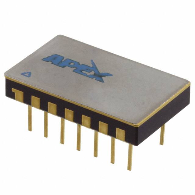
♦ Hermetic 14-pin Ceramic DIP
♦ Military Processing Option
APPLICATIONS
♦ Precision A/D and D/A Converters
♦ Transducer Excitation
♦ Accurate Comparator Threshold Reference
♦ High Resolution Servo Systems
♦ Digital Voltmeters
♦ High Precision Test and Measurement Instruments
DESCRIPTION
VRE107 Series Precision Voltage References provide
ultrastable ±5 V outputs with ±0.8 mV initial accuracy
and temperature coefficient as low as 1.33 ppm/°C
over the full military temperature range. This impovement in accuracy is made possible by a unique, proprietary multipoint laser compensation technique.
Significant improvements have been made in other
performance parameters as well, including initial accuracy, warm-up drift, line regulation, and long-term
stability, making the VRE107 series the most accurate
and stable 5 V references available.
VRE107 series devices are available in two performance grades. All devices are packaged in 14-pin
hermetic ceramic packages for maximum long-term
stablity. “M” versions are screened for high reliability
and quality.
Superior stability, accuracy, and quality make these
references ideal for precision applications such as A/D
and D/A converters, high accuracy test and measurement instrumentation, and tranducer excitation.
Figure 1. BLOCK DIAGRAM
www.apexanalog.com
VRE107DS
Copyright © Apex Microtechnology, Inc. 2012
(All Rights Reserved)
SEP 2012
1
VRE107DS REVH
�VRE107
SELECTION GUIDE
Model
Output (V)
Temperature
Operating Range
Volt Deviation (MAX)
±5
±5
-55°C to +125°C
-55°C to +125°C
±0.7mV
±0.6mV
VRE107M
VRE107MA
1. CHARACTERISTICS AND SPECIFICATIONS
Hermetic 14-pin Ceramic DIP
Package Style HC
ELECTRICAL SPECIFICATIONS
VPS =±15V, T = +25°C, RL = 10K Ω UNLESS OTHERWISE NOTED.
Model
Parameter
VRE107M
Min
Typ
VRE107MA
Max
Min
Typ
Max
Units
ABSOLUTE MAXIMUM RATINGS
Power Supply
±13.5
±22
*
*
V
Operating Temperature
-55
+125
*
*
ºC
Storage Temperature
-65
+150
*
*
ºC
Short Circuit Protection
Continuous
*
±5
*
OUTPUT VOLTAGE
VRE107
V
OUTPUT VOLTAGE ERRORS
Initial Error
±900
Warmup Drift
TMIN - TMAX
±800
2
(Note1)
1
700
µV
ppm
600
µV
Long-Term Stability
6
*
ppm/1000hrs.
Noise (0.1 - 10Hz)
3
*
µVpp
OUTPUT CURRENT
Range
±10
*
mA
REGULATION
Line
6
10
*
*
ppm/V
Load
3
*
ppm/mA
Range
10
*
mV
Temperature Coefficient
4
*
µV/ºC/mV
OUTPUT ADJUSTMENT
POWER SUPPLY CURRENT (Note 2)
VRE107 +PS
7
9
*
*
mA
VRE107 -PS
4
6
*
*
mA
NOTES:
* Same as M Models.
1. Using the box method, the specified value is the maximum deviation from the output voltage at 25°C
over the specified operating temperature range.
2. The specified values are unloaded.
2
VRE107DS
�VRE107
TYPICAL PERFORMANCE GRAPHS
VOUT vs. TEMPERATURE
0.7
VOUT vs. TEMPERATURE
0.6
-0.6
-0.7
Temperature oC
VRE107M
Temperature oC
VRE107MA
POSITIVE OUTPUT
QUIESCENT CURRENT VS. TEMP
Temperature oC
JUNCTION TEMP. RISE VS. OUTPUT CURRENT
Output Current (mA)
PSRR VS. FREQUENCY
Frequency (Hz)
NEGATIVE OUTPUT
QUIESCENT CURRENT VS. TEMP
Temperature oC
JUNCTION TEMP. RISE VS. OUTPUT CURRENT
Output Current (mA)
PSRR VS. FREQUENCY
Frequency (Hz)
2. THEORY OF OPERATION
The following discussion refers to the block diagram in Figure 1. A FET current source is used to bias a 6.3 V zener
diode. The zener voltage is divided by the resistor network R1 and R2. This voltage is then applied to the noninverting input of the operational amplifier which amplifies the voltage to produce a 5 V output. The gain is determined by
the resistor networks R3 and R4: G=1 + R4/R3. The 6.3 V zener diode is used because it is the most stable diode
over time and temperature.
The current source provides a closely regulated zener current, which determines the slope of the reference’s voltage vs. temperature function. By trimming the zener current, a lower drift over temperature can be achieved. But
since the voltage vs. temperature function is nonlinear, this method leaves a residual error over wide temperature
ranges.
To remove this residual error, a nonlinear compensation network of thermistors and resistors is used in the VRE107
VRE107DS
3
�VRE107
series references. This proprietary network eliminates most of the nonlinearity in the voltage vs. temperature function. By then adjusting the slope, The VRE107 series produces a very stable voltage over wide temperature ranges.
This network is less than 2% of the overall network resistance so it has a negligible effect on long term stability.
3. APPLICATION INFORMATION
The proper connection of the VRE107 series voltage reference is shown below with the optional trim resistors.
When trimming the VRE107, the positive voltage should be trimmed first since the negative voltage tracks the positive side. Pay careful attention to the circuit layout to avoid noise pickup and voltage drops in the lines.
The VRE107 series voltage references have the ground terminal brought out on two pins (pin 6 and pin 7) which
are connected together internally. This allows the user to achieve greater accuracy when using a socket. Voltage
references have a voltage drop across their power supply ground pin due to quiescent current flowing through the
contact resistance. If the contact resistance was constant with time and temperature, this voltage drop could be
trimmed out. When the reference is plugged into a socket, this source of error can be as high as 20 ppm. By connecting pin 7 to the power supply ground and pin 6 to a high impedance ground point in the measurement circuit,
the error due to the contact resistance can be eliminated. If the unit is soldered into place the contact resistance is
sufficiently small that it doesn’t effect performance.
EXTERNAL CONNECTIONS
PIN CONFIGURATION
TOP VIEW
FINE +ADJ.
FINE -ADJ.
-5V
+5V
FINE +ADJ.
FINE -ADJ.
-PS
VRE107
NC
3. Optional Fine Adjust for approximately ±10mV.
+PS
NC
REF. GND
NC
GND
NC
NEED TECHNICAL HELP? CONTACT APEX SUPPORT!
For all Apex Microtechnology product questions and inquiries, call toll free 800-546-2739 in North America.
For inquiries via email, please contact apex.support@apexanalog.com.
International customers can also request support by contacting their local Apex Microtechnology Sales Representative.
To find the one nearest to you, go to www.apexanalog.com
IMPORTANT NOTICE
Apex Microtechnology, Inc. has made every effort to insure the accuracy of the content contained in this document. However, the information is subject to change
without notice and is provided "AS IS" without warranty of any kind (expressed or implied). Apex Microtechnology reserves the right to make changes without further
notice to any specifications or products mentioned herein to improve reliability. This document is the property of Apex Microtechnology and by furnishing this information, Apex Microtechnology grants no license, expressed or implied under any patents, mask work rights, copyrights, trademarks, trade secrets or other intellectual
property rights. Apex Microtechnology owns the copyrights associated with the information contained herein and gives consent for copies to be made of the information only for use within your organization with respect to Apex Microtechnology integrated circuits or other products of Apex Microtechnology. This consent does not
extend to other copying such as copying for general distribution, advertising or promotional purposes, or for creating any work for resale.
APEX MICROTECHNOLOGY PRODUCTS ARE NOT DESIGNED, AUTHORIZED OR WARRANTED TO BE SUITABLE FOR USE IN PRODUCTS USED FOR
LIFE SUPPORT, AUTOMOTIVE SAFETY, SECURITY DEVICES, OR OTHER CRITICAL APPLICATIONS. PRODUCTS IN SUCH APPLICATIONS ARE UNDERSTOOD TO BE FULLY AT THE CUSTOMER OR THE CUSTOMER’S RISK.
Apex Microtechnology, Apex and Apex Precision Power are trademarks of Apex Microtechnolgy, Inc. All other corporate names noted herein may be trademarks
of their respective holders.
www.apexanalog.com
4
Copyright © Apex Microtechnology, Inc. 2012
(All Rights Reserved)
SEP 2012
VRE107DS
VRE107DS REVH
�
很抱歉,暂时无法提供与“VRE107MA”相匹配的价格&库存,您可以联系我们找货
免费人工找货