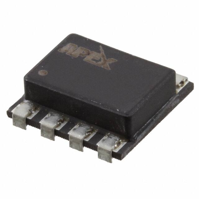
VRE3050
RoHS
Precision Voltage Reference
COMPLIANT
FEATURES
•
•
•
•
•
•
•
•
+5 V Output, ± 0.5 mV (0.01%)
Temperature Drift: 0.6 ppm/°C
Low Noise: 3 μVP-P (0.1 Hz - 10 Hz)
Low Thermal Hysteresis: 1 ppm Typical
±15mA Output Source and Sink Current
Excellent Line Regulation: 5 ppm/V Typical
Optional Noise Reduction and Voltage Trim
Industry Standard Pinout: 8-pin Surface Mount Package
APPLICATIONS
The VRE3050 is recommended for use as a reference for 14, 16, or 18 bit data converters which require
an external precision reference. The device is also ideal for calibrating scale factor on high resolution data
converters. The VRE3050 offers superior performance over monolithic references.
DESCRIPTION
The VRE3050 is a low cost, high precision 5 V reference that operates from +10 V. The device features a
buried zener for low noise and excellent long term stability. Packaged in an 8-pin SMT, the device is ideal for
high resolution data conversion systems.
The device provides ultrastable +5 V output with ±0.5 mV (0.01%) initial accuracy and a temperature
coefficient of 0.6 ppm/°C. This improvement in accuracy is made possible by a unique, patented multi-point
laser compensation technique. Significant improvements have been made in other performance parameters
as well, including initial accuracy, warm-up drift, line regulation, and long-term stability, making the VRE3050
series the most accurate reference available.
For enhanced performance, the VRE3050 has an external trim option for users who want less than 0.01%
initial error. For ultra low noise applications, an external capacitor can be attached between the noise reduction pin and the ground pin. A ceramic input filter capacitor of 0.1μF is recommended to ensure output stability.
SELECTION GUIDE
Model
www.apexanalog.com
Initial Error
(mV)
Temp. Coeff.
(ppm/ºC)
Temp Range
(ºC)
VRE3050BS
±0.8
1.0
0ºC to +70ºC
VRE3050JS
±0.5
0.6
-40ºC to +85ºC
VRE3050LS
±1.0
2.0
-40ºC to +85ºC
© Apex Microtechnology Inc.
All rights reserved
Oct 2017
VRE3050DS Rev O
�VRE3050
TYPICAL CONNECTION
Figure 1: Typical Connection
+ V IN
2
Optional
Noise
Reduction
Capacitor
Input Filter
Capacitor
CIN
0.1μF
+ V OUT
8
6
VRE3025
CN
5
1μF
4
10 kΩ
Optional Fine
Trim Adjustment
GND
PIN DESCRIPTIONS
2
Pin Number
Name
Description
1, 3, 7
NC
No connection.
2
VIN
The supply voltage connection.
4
GND
Ground.
5
TRIM
Optional fine adjustment. Connect to a voltage divider between OUT and GND.
6
OUT
5 V output.
8
NR
Optional noise reduction. Connect a 1µF capacitor between this pin and GND.
VRE3050DS Rev O
�VRE3050
ELECTRICAL SPECIFICATIONS
ABSOLUTE MAXIMUM RATINGS
Parameter
Power Supply
Symbol
Min
Max
Unit
VIN
-0.3
+40
V
-0.3
+12
V
-0.3
+6
V
0
+70
°C
-40
Out, Trim
Noise Reduction
Operating Temp. (B)
Operating Temp. (J, L)
NR
+85
°C
Out Short Circuit to GND Duration (VIN
很抱歉,暂时无法提供与“VRE3050JS”相匹配的价格&库存,您可以联系我们找货
免费人工找货