Features
• 8-Bit Multiplexed Addresses/Outputs • Fast Read Access Time - 90 ns • Dual Voltage Range Operation • • • • • • •
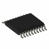
– Low-Voltage Power Supply Range, 3.0V to 3.6V, or – Standard 5V ± 10% Supply Range Low Power CMOS Operation – 20 µA max. Standby for ALE = VIH and VCC = 3.6V – 29 mW max. Active at 5 MHz for VCC = 3.6V 20-Lead TSSOP Package High Reliability CMOS Technology – 2,000V ESD Protection – 200 mA Latchup Immunity Rapid™ Programming Algorithm - 50 µs/byte (typical) CMOS and TTL Compatible Inputs and Outputs – JEDEC Standard for LVTTL Integrated Product Identification Code Commercial and Industrial Temperature Range
Description
The AT27LV520 is a low-power, high-performance 524,288-bit one-time programmable read only memory (OTP EPROM) organized 64K by 8 bits. It incorporates latches for the 8 lower order address bits to multiplex with the 8 data bits. This minimizes system chip count, reduces cost, and simplifies the design of multiplexed bus systems. It requires only one power supply in the range of 3.0V to 3.6V for normal read mode operation, making it ideal for fast, portable systems using battery power. Any byte can be accessed in less than 90 ns. The AT27LV520 is available in 173 mil, 20-pin TSSOP, 300 mil, 20-pin SOIC and 28pin TSOP, one-time programmable (OTP) plastic packages. (continued)
512K (64K x 8) Multiplexed Addresses/ Outputs Low Voltage OTP EPROM AT27LV520
Pin Configurations
Pin Name A8 - A15 AD0 - AD7 OE /VPP ALE Function Addresses Addresses/Outputs Output Enable/VPP Address Latch Enable
TSOP Top View
A10 NC NC A12 A14 ALE VCC OE/VPP A15 A13 A11 NC NC A9 22 23 24 25 26 27 28 1 2 3 4 5 6 7 21 20 19 18 17 16 15 14 13 12 11 10 9 8 A8 NC NC AD1 AD3 AD5 AD7 GND AD6 AD4 AD2 NC NC AD0
TSSOP Top View
A10 A12 A14 ALE VCC OE/VPP A15 A13 A11 A9 1 2 3 4 5 6 7 8 9 10 20 19 18 17 16 15 14 13 12 11 A8 AD1 AD3 AD5 AD7 GND AD6 AD4 AD2 AD0
SOIC Top View
OE/VPP A15 A13 A11 A9 AD0 AD2 AD4 AD6 GND 1 2 3 4 5 6 7 8 9 10 20 19 18 17 16 15 14 13 12 11 VCC ALE A14 A12 A10 A8 AD1 AD3 AD5 AD7
Rev. 0911B-B–01/98
1
�Atmel’s innovative design techniques provide fast speeds that rival 5V parts while keeping the low power consumption of a 3.3V supply. At V CC = 3 .0V, any byte can be accessed in less than 90 ns. With a typical power dissipation of only 18 mW at 5 MHz and V C C = 3 .3V, the AT27LV520 consumes less than one fifth the power of a standard 5V EPROM. Standby mode is acheived by asserting ALE high. Standby mode supply current is typically less than 1 µA at 3.3V. The AT27LV520 operating with VCC at 3.0V produces TTL level outputs that are compatible with standard TTL logic devices operating at VCC = 5.0V. The device is also capable of standard 5-volt operation making it ideally suited for dual supply range systems or card products that are pluggable in both 3-volt and 5-volt hosts. Atmel’s AT27LV520 has additional features to ensure high quality and efficient production use. The Rapid™ Programming Algorithm reduces the time required to program the part and guarantees reliable programming. Programing time is typically only 50 µs/byte. The Integrated Product Identification Code electronically identifies the device and
manufacturer. This feature is used by industry standard programming equipment to select the proper programming algorithms and voltages. The AT27LV520 programs exactly the same way as a standard 5V AT27C520 and uses the same programming equipment.
System Considerations
Switching under active conditions may produce transient voltage excursions. Unless accommodated by the system design, these transients may exceed data sheet limits, resulting in device non-conformance. At a minimum, a 0.1 µ F high frequency, low inherent inductance, ceramic capacitor should be utilized for each device. This capacitor should be connected between the VCC and Ground terminals of the device, as close to the device as possible. Additionally, to stabilize the supply voltage level on printed circuit boards with large EPROM arrays, a 4.7 µF bulk electrolytic capacitor should be utilized, again connected between the V CC a nd Ground terminals. This capacitor should be positioned as close as possible to the point where the power supply is connected to the array.
Block Diagram
VCC GND OE/VPP ALE OE, ALE, AND PROGRAM LOGIC OUTPUT BUFFERS 8
LATCHES
Y DECODER
Y-GATING
AD7 - AD0
A15 - A8
8
X DECODER
CELL MATRIX
IDENTIFICATION
2
AT27LV520
�AT27LV520
Absolute Maximum Ratings*
Temperature Under Bias ................................ -55°C to +125°C Storage Temperature ..................................... -65°C to +150°C Voltage on Any Pin with Respect to Ground ........................................ -2.0V to +7.0V(1) Voltage on A9 with Respect to Ground ..................................... -2.0V to +14.0V(1) Note: VPP Supply Voltage with Respect to Ground ...................................... -2.0V to +14.0V(1) 1. *NOTICE: Stresses beyond those listed under “Absolute Maximum Ratings” may cause permanent damage to the device. This is a stress rating only and functional operation of the device at these or any other conditions beyond those indicated in the operational sections of this specification is not implied. Exposure to absolute maximum rating conditions for extended periods may affect device reliability. Minimum voltage is -0.6V DC which may undershoot to -2.0V for pulses of less than 20 ns. Maximum output pin voltage is VCC + 0.75V DC which may overshoot to +7.0V for pulses of less than 20 ns.
Operating Modes
Mode/Pin Read(2) Output Disable(2) Enable(2) ALE VIL VIL/VIH VIH VIH VIH
(4)
OE/VPP VIL VIH VIH VIH VPP VIL
A8 - A15 Ai X(1) Ai X Ai A9 = VH A8 = VIH or VIL A10 - A15 = VIL
(5)
AD0 - AD7 DOUT High Z/A0 - A7 A0 - A7 A0 - A7 DIN Identification Code
Standby Address Latch Rapid Program(3) Product Identification
Notes:
VIL
1. X can be VIL or VIH. 2. Read, output disable, and standby modes require 3.0V ≤ VCC ≤ 3.6V, or 4.5V ≤ VCC ≤ 5.5V. 3. Refer to Programming Characteristics. 4. VH = 12.0 ± 0.5V. 5. Two identifier bytes may be selected. All A8 - A15 inputs are held low (VIL), except A9 which is set to VH and A8 which is toggled low (VIL) to select the Manufacturer’s Identification byte and high (VIH) to select the Device Code byte.
3
�DC and AC Operating Conditions for Read Operation
AT27LV520-90 Com. Operating Temp. (Case) Ind. VCC Supply -40°C - +85°C 3.0V to 3.6V 5V ± 10% 0°C - 70°C
DC and Operating Characteristics for Read Operation
Symbol Parameter Condition Min Max Units
VCC = 3.0V to 3.6V
ILI ILO ISB ICC VIL VIH VOL VOH
(1)
Input Load Current Output Leakage Current VCC Standby Current VCC Active Current Input Low Voltage Input High Voltage Output Low Voltage Output High Voltage
VIN = 0V to VCC VOUT = 0V to VCC ALE = VCC ± 0.3V; Ai, ADi = GND/VCC ± 0.3V f = 5 MHz, IOUT = 0 mA, ALE = VIL -0.6 2.0 IOL = 2.0 mA IOH = -2.0 mA 2.4
±1 ±5 20 8 0.8 VCC + 0.5 0.4
µA µA µA mA V V V V
VCC = 4.5V to 5.5V ILI ILO ISB ICC VIL VIH VOL VOH
(1)
Input Load Current Output Leakage Current VCC Standby Current VCC Active Current Input Low Voltage Input High Voltage Output Low Voltage Output High Voltage
VIN = 0V to VCC VOUT = 0V to VCC ALE = VCC ± 0.3V; Ai, ADi = GND/VCC ± 0.3V f = 5 MHz, IOUT = 0 mA, ALE = VIL -0.6 2.0 IOL = 2.1 mA IOH = -400 µA 2.4
±1 ±5 100 20 0.8 VCC + 0.5 0.4
µA µA µA mA V V V
Note:
VCC standby current will be slightly higher with ALE, Ai, and ADi at TTL levels.
AC Characteristics for Read Operation
VCC = 3.0V to 3.6V and 4.5V to 5.5V
AT27LV520-90 Symbol tACC tCE tAS tAH tALE tOE(3) tDF(4)(5) tOH
(3)
Parameter Address to Output Delay Address Latch Enable Low to Output Delay Address Setup Time Address Hold Time Address Latch Enable Width OE/VPP to Output Delay OE/VPP High to Output Float Output Hold from Address or OE/VPP whichever occurred first ,
Condition ALE = OE/VPP = VIL Address Valid OE/VPP = VIH OE/VPP = VIH OE/VPP = VIH ALE = VIL ALE = VIL ALE = VIL
Min
Max 90 70
Units ns ns ns ns ns
15 15 45 35 25 0
ns ns ns
Notes:
2, 3, 4 — see AC Waveforms for Read Operation
4
AT27LV520
�AT27LV520
AC Waveforms for Read Operation(1)
tALE ALE tCE OE/VPP tDF tAS AD7 - AD0 ADDRESS IN tACC A15 - A8
Notes: 1. 2. 3. 4. 5. Timing measurement reference levels for all speed grades are VOL = 0.8V and VOH = 2.0V. Input AC drive levels are VIL = 0.45V and VIH = 2.4V. OE/VPP may be delayed up to tCE - tOE after the address is valid without impact on tCE. OE/VPP may be delayed up to tACC - tOE after the address is valid without impact on tACC. This parameter is only sampled and is not 100% tested. Output float is defined as the point when data is no longer driven.
tAH
tOE
tOH DATA OUT
Input Test Waveforms and Measurement Levels
Output Test Load
tR, tF < 20 ns (10% to 90%)
Note:
CL = 100 pF including jig capacitance.
Pin Capacitance(Note:)
(f = 1 MHz, T = 25°C) Typ CIN COUT
Note:
Max 6 12
Units pF pF
Conditions VIN = 0V VOUT = 0V
4 8
Typical values for nominal supply voltage. This parameter is only sampled and is not 100% tested.
5
�Programming Waveforms
PROGRAM VCC 6.5V 5.0V tVCS 13V OE/VPP VIH VIL tPRT ALE VIH VIL tLP tALE tLAS ADDR tAS A15 - A8 VIH VIL ADDRESS STABLE tLAH tPW tDS DATA IN tDH tALE tOE AD7 - AD0 VIH VIL tLAS ADDR tLAH DATA OUT tAH tDFP tOES tOEH tVR READ (VERIFY)
Notes:
1. 2.
The Input Timing Reference is 0.8V for VIL and 2.0V for VIH. tOE and tDFP are characteristics of the device but must be accommodated by the programmer.
DC Programming Characteristics
TA = 25 ± 5°C, VCC = 6.5 ± 0.25V, OE/VPP = 13.0 ± 0.25V Limits Symbol ILI VIL VIH VOL VOH ICC2 IPP2 Parameter Input Load Current Input Low Level Input High Level Output Low Voltage Output High Voltage VCC Supply Current (Program and Verify) OE/VPP Current ALE = VIH IOL = 2.1 mA IOH = -400 µA 2.4 25 25 Test Conditions VIN = VIL, VIH -0.6 2.0 Min Max ±10 0.8 VCC + 1.0 0.4 Units µA V V V V mA mA
6
AT27LV520
�AT27LV520
AC Programming Characteristics*
TA = 25 ± 5°C, VCC = 6.5 ± 0.25V, OE/VPP = 13.0 ± 0.25V Limits Symbol tALE tLAS tLAH tLP tOES tOEH tDS tDH tPW tVR tVCS tOE tDFP tAS tAH tPRT
Notes:
Parameter(1) Address Latch Enable Width Latched Address Setup Time Latched Address Hold Time ALE Low to OE/VPP High Voltage Delay OE/VPP Setup Time OE/VPP Hold Time Data Setup Time Data Hold Time ALE Program Pulse Width(2)
Test Conditions
Min 500 100 100 2
Max
Units ns ns ns µs µs µs µs µs µs µs µs
Input Rise and Fall Times (10% to 90%) 20 ns Input Pulse Levels 0.45V to 2.4V Input Timing Reference Level 0.8V to 2.0V Output Timing Reference Level 0.8V to 2.0V
2 2 2 2 47.5 2 2 150 0 2 0 50 130 52.5
OE/VPP Recovery Time VCC Setup Time Data Valid from OE/VPP OE/VPP High to Output Float Address Setup Time Address Hold Time OE/VPP Pulse Rise Time During Programming
2. Program Pulse width tolerance is 50 µsec ± 5%.
ns ns µs µs ns
Delay(4)
1. VCC must be applied simultaneously or before OE/VPP and removed simultaneously or after OE/VPP .
3. This parameter is only sampled and is not 100% tested. Output Float is defined as the point where data is no longer driven — see timing diagram.
Atmel’s 27LV520 Integrated Product Identification Code
Pins Codes Manufacturer Device Type A8 0 1 AD7 0 1 AD6 0 0 AD5 0 0 AD4 1 1 AD3 1 1 AD2 1 1 AD1 1 0 AD0 0 1
Hex Data
1E 9D
7
�Rapid™ Programming Algorithm
A 50 µs ALE pulse width is used to program. The address is set to the first location. VCC is raised to 6.5V and OE/VPP is raised to 13.0V. Each address is first programmed with one 50 µs ALE pulse without verification. Then a verification/reprogramming loop is executed for each address. In the event a byte fails to pass verification, up to 10 successive 50 µs pulses are applied with a verification after each
pulse. If the byte fails to verify after 10 pulses have been applied, the part is considered failed. After the byte verifies properly, the next address is selected until all have been checked. OE/VPP is then lowered to VIH and VCC to 5.0V. All bytes are read again and compared with the original data to determine if the device passes or fails.
START
ADDR = FIRST LOCATION VCC = 6.5V VPP = 13.0V PROGRAM ONE 50 µS PULSE
INCREMENT ADDRESS
NO
LAST ADDR.? YES
ADDR = FIRST LOCATION INCREMENT ADDRESS NO LAST ADDR.? YES PROGRAM ONE 100 µS PULSE NO X = 10? PASS VERIFY BYTE FAIL INCREMENT X X=0
YES
VCC = 5.0V VPP = 5.0V
COMPARE ALL BYTES TO ORIGINAL DATA
FAIL
DEVICE FAILED
PASS DEVICE PASSED
8
AT27LV520
�AT27LV520
Ordering Information
tACC (ns) 90 ICC (mA) Active 8 Ordering Code AT27LV520-90SC AT27LV520-90TC AT27LV520-90XC AT27LV520-90SI AT27LV520-90TI AT27LV520-90XI Package 20S 28T 20X 20S 28T 20X Operation Range Commercial (0°C to 70°C) Industrial (-40°C to +85°C)
90
8
Package Type 20S 28T 20X 20-Lead, 0.300” Wide, Plastic Gull-Wing Small Outline (SOIC) 28-Lead, Thin Small Outline Package (TSOP) 20-Lead, 0.173” Wide, Thin Shrink Small Outline (TSSOP)
9
�Packaging Information
20S, 20-Lead, 0.300” Wide, Plastic Gull Wing Small Outline Dimensions in Inches and (Millimeters) 28T, 28-Lead, Plastic Thin Small Outline Package (TSOP) Dimensions in Millimeters and (Inches)
.020(.508) .013(.330)
.299(7.60) .420(10.7) .291(7.39) .393(9.98) PIN 1 ID
.050(1.27) BSC .513(13.0) .497(12.6)
.105(2.67) .092(2.34)
.012(.305) .003(.076)
.013(.330) .009(.229) 0 REF 8 .035(0.889) .015(.381)
20X, 20-Lead, 0.173” Wide, Thin Super Small Outline Package (TSSOP) Dimensions in (Millimeters) and Inches
0.30(0.012) 0.18(0.007)
4.48(.176) 6.50(.256) 4.30(.169) 6.25(.246) PIN 1 ID
0.65(.0256) BSC 6.60(.260) 6.40(.252)
1.10(0.043) MAX
0.15(.006) 0.05(.002)
0.18(.007) 0.09(.003) 0 REF 8 0.70(.028) 0.50(.020)
10
AT27LV520
�