Features
• • • • • • • • • • •
Compatible with MCS-51™ Products 4K Bytes of User Programmable QuickFlash Memory 2.7V to 5.5V Operating Range Fully Static Operation: 0 Hz to 16 MHz Three-level Program Memory Lock 128 x 8-bit Internal RAM 32 Programmable I/O Lines Two 16-bit Timer/Counters Six Interrupt Sources Programmable Serial Channel Low-power Idle and Power-down Modes
Description
The AT87LV51 is a low-voltage, high-performance CMOS 8-bit microcontroller with 4K bytes of QuickFlash One-Time Programmable (OTP) Read Only memory. The device is manufactured using Atmel’s high-density nonvolatile memory technology and is compatible with the industry standard MCS-51 instruction set and pinout. The on-chip QuickFlash allows the program memory to be user programmed by a conventional nonvolatile memory programmer. By combining a versatile 8-bit CPU with QuickFlash on a monolithic chip, the Atmel AT87LV51 is a powerful microcontroller that provides a highly flexible and cost-effective solution to many embedded control applications. (continued)
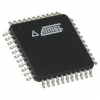
P1.4 P1.3 P1.2 P1.1 P1.0 NC VCC P0.0 (AD0) P0.1 (AD1) P0.2 (AD2) P0.3 (AD3)
8-bit Microcontroller with 4K Bytes QuickFlash® AT87LV51 Preliminary
Pin Configurations
P1.5 P1.6 P1.7 RST (RXD) P3.0 NC (TXD) P3.1 (INT0) P3.2 (INT1) P3.3 (T0) P3.4 (T1) P3.5 1 2 3 4 5 6 7 8 9 10 11
TQFP
44 43 42 41 40 39 38 37 36 35 34
PDIP
P1.0 P1.1 P1.2 P1.3 P1.4 P1.5 P1.6 P1.7 RST (RXD) P3.0 (TXD) P3.1 (INT0) P3.2 (INT1) P3.3 (T0) P3.4 (T1) P3.5 (WR) P3.6 (RD) P3.7 XTAL2 XTAL1 GND 1 2 3 4 5 6 7 8 9 10 11 12 13 14 15 16 17 18 19 20 40 39 38 37 36 35 34 33 32 31 30 29 28 27 26 25 24 23 22 21 VCC P0.0 (AD0) P0.1 (AD1) P0.2 (AD2) P0.3 (AD3) P0.4 (AD4) P0.5 (AD5) P0.6 (AD6) P0.7 (AD7) EA/VPP ALE/PROG PSEN P2.7 (A15) P2.6 (A14) P2.5 (A13) P2.4 (A12) P2.3 (A11) P2.2 (A10) P2.1 (A9) P2.0 (A8)
33 32 31 30 29 28 27 26 25 24 23
12 13 14 15 16 17 18 19 20 21 22
P0.4 (AD4) P0.5 (AD5) P0.6 (AD6) P0.7 (AD7) EAVPP NC ALE/PROG PSEN P2.7 (A15) P2.6 (A14) P2.5 (A13)
6 5 4 3 2 1 44 43 42 41 40
P1.4 P1.3 P1.2 P1.1 P1.0 NC VCC P0.0 (AD0) P0.1 (AD1) P0.2 (AD2) P0.3 (AD3) (WR) P3.6 (RD) P3.7 XTAL2 XTAL1 GND NC (A8) P2.0 (A9) P2.1 (A10) P2.2 (A11) P2.3 (A12) P2.4 18 19 20 21 22 23 24 25 26 27 28
(WR) P3.6 (RD) P3.7 XTAL2 XTAL1 GND GND (A8) P2.0 (A9) P2.1 (A10) P2.2 (A11) P2.3 (A12) P2.4
PLCC
P1.5 P1.6 P1.7 RST (RXD) P3.0 NC (TXD) P3.1 (INT0) P3.2 (INT1) P3.3 (T0) P3.4 (T1) P3.5
7 8 9 10 11 12 13 14 15 16 17
39 38 37 36 35 34 33 32 31 30 29
P0.4 (AD4) P0.5 (AD5) P0.6 (AD6) P0.7 (AD7) EA/VPP NC ALE/PROG PSEN P2.7 (A15) P2.6 (A14) P2.5 (A13)
Rev. 1602A–04/00
1
�Block Diagram
2
AT87LV51
�AT87LV51
The AT87LV51 provides the following standard features: 4K bytes of QuickFlash OTP program memory, 128 bytes of RAM, 32 I/O lines, two 16-bit timer/counters, a five-vector, 2-level interrupt architecture, a full duplex serial port, on-chip oscillator, and clock circuitry. In addition, the AT87LV51 is designed with static logic for operation down to zero frequency and supports two software-selectable power-saving modes. The Idle mode stops the CPU while allowing the RAM, timer/counters, serial port and interrupt system to continue functioning. The Power-down mode saves the RAM contents but freezes the oscillator disabling all other chip functions until the next hardware reset. Port 2 emits the high-order address byte during fetches from external program memory and during accesses to external data memory that use 16-bit addresses (MOVX @ DPTR). In this application, it uses strong internal pull-ups when emitting 1s. During accesses to external data memory that use 8-bit addresses (MOVX @ RI), Port 2 emits the contents of the P2 Special Function Register. Port 2 also receives the high-order address bits and some control signals during QuickFlash programming and verification. Port 3 Port 3 is an 8-bit bidirectional I/O port with internal pull-ups. The Port 3 output buffers can sink/source four TTL inputs. When 1s are written to Port 3 pins they are pulled high by the internal pull-ups and can be used as inputs. As inputs, Port 3 pins that are externally being pulled low will source current (IIL) because of the pull-ups. Port 3 also serves the functions of various special features of the AT87LV51 as listed below:
Pin Description
VCC Supply voltage. GND Ground. Port 0 Port 0 is an 8-bit open drain bidirectional I/O port. As an output port, each pin can sink eight TTL inputs. When 1s are written to Port 0 pins, the pins can be used as highimpedance inputs. Port 0 may also be configured to be the multiplexed loworder address/data bus during accesses to external program and data memory. In this mode, P0 has internal pull-ups. Port 0 also receives the code bytes during QuickFlash programming and outputs the code bytes during program verification. External pull-ups are required during program verification. Port 1 Port 1 is an 8-bit bidirectional I/O port with internal pull-ups. The Port 1 output buffers can sink/source four TTL inputs. When 1s are written to Port 1 pins they are pulled high by the internal pull-ups and can be used as inputs. As inputs, Port 1 pins that are externally being pulled low will source current (IIL) because of the internal pull-ups. Port 1 also receives the low-order address bytes during QuickFlash programming and verification. Port 2 Port 2 is an 8-bit bidirectional I/O port with internal pull-ups. The Port 2 output buffers can sink/source four TTL inputs. When 1s are written to Port 2 pins they are pulled high by the internal pull-ups and can be used as inputs. As inputs, Port 2 pins that are externally being pulled low will source current (IIL) because of the internal pull-ups.
Port Pin P3.0 P3.1 P3.2 P3.3 P3.4 P3.5 P3.6 P3.7
Alternate Functions RXD (serial input port) TXD (serial output port) INT0 (external interrupt 0) INT1 (external interrupt 1) T0 (timer 0 external input) T1 (timer 1 external input) WR (external data memory write strobe) RD (external data memory read strobe)
Port 3 also receives some control signals for QuickFlash programming and verification. RST Reset input. A high on this pin for two machine cycles while the oscillator is running resets the device. ALE/PROG Address Latch Enable output pulse for latching the low byte of the address during accesses to external memory. This pin is also the program pulse input (PROG) during QuickFlash programming. In normal operation ALE is emitted at a constant rate of 1/6 the oscillator frequency and may be used for external timing or clocking purposes. Note, however, that one ALE pulse is skipped during each access to external data memory.
3
�PSEN Program Store Enable is the read strobe to external program memory. When the AT87LV51 is executing code from external program memory, PSEN i s activated twice each machine cycle, except that two PSEN activations are skipped during each access to external data memory. EA/VPP External Access Enable. EA must be strapped to GND in order to enable the device to fetch code from external program memory locations starting at 0000H, up to FFFFH. Note, however, that if lock bit 1 is programmed, EA will be internally latched on reset.
EA s hould be strapped to VCC for internal program executions. This pin also receives the 12-volt programming enable voltage (VPP) during QuickFlash programming. XTAL1 Input to the inverting oscillator amplifier and input to the internal clock operating circuit. XTAL2 Output from the inverting oscillator amplifier.
Special Function Registers
A map of the on-chip memory area called the Special Function Register (SFR) space is shown in Table 1.
Table 1. AT87LV51 SFR Map and Reset Values
0F8H 0F0H 0E8H 0E0H 0D8H 0D0H 0C8H 0C0H 0B8H 0B0H 0A8H 0A0H 98H 90H 88H 80H IP XX000000 P3 11111111 IE 0X000000 P2 11111111 SCON 00000000 P1 11111111 TCON 00000000 P0 11111111 TMOD 00000000 SP 00000111 TL0 00000000 DPL 00000000 TL1 00000000 DPH 00000000 TH0 00000000 TH1 00000000 PCON 0XXX0000 SBUF XXXXXXXX PSW 00000000 ACC 00000000 B 00000000 0FFH 0F7H 0EFH 0E7H 0DFH 0D7H 0CFH 0C7H 0BFH 0B7H 0AFH 0A7H 9FH 97H 8FH 87H
4
AT87LV51
�AT87LV51
Note that not all of the addresses are occupied, and unoccupied addresses may not be implemented on the chip. Read accesses to these addresses will, in general, return random data and write accesses will have an indeterminate effect. User software should not write 1s to these unlisted locations, since they may be used in future products to invoke new features. In that case, the reset or inactive values of the new bits will always be 0. Timer 0 and 1 Timer 0 and Timer 1 in the AT87LV51 operate the same way as Timer 0 and Timer 1 in the AT89C51. Figure 2. External Clock Drive Configuration
NC XTAL2
EXTERNAL OSCILLATOR SIGNAL
XTAL1
GND
Oscillator Characteristics
XTAL1 and XTAL2 are the input and output, respectively, of an inverting amplifier, which can be configured for use as an on-chip oscillator as shown in Figure 1. Either a quartz crystal or ceramic resonator may be used. To drive the device from an external clock source, XTAL2 should be left unconnected while XTAL1 is driven as shown in Figure 2. There are no requirements on the duty cycle of the external clock signal, since the input to the internal clocking circuitry is through a divide-by-two flip-flop, but minimum and maximum voltage high and low time specifications must be observed. Figure 1. Oscillator Connections
C2 XTAL2
Idle Mode
In Idle Mode, the CPU puts itself to sleep while all the onchip peripherals remain active. The mode is invoked by software. The content of the on-chip RAM and all the Special Function registers remains unchanged during this mode. The Idle mode can be terminated by any enabled interrupt or by a hardware reset. It should be noted that when Idle is terminated by a hardware reset, the device normally resumes program execution from where it left off, up to two machine cycles before the internal reset algorithm takes control. On-chip hardware inhibits access to internal RAM in this event, but access to the port pins is not inhibited. To eliminate the possibility of an unexpected write to a port pin when Idle is terminated by reset, the instruction following the one that invokes Idle should not be one that writes to a port pin or to external memory.
C1 XTAL1
Power-down Mode
In Power-down Mode, the oscillator is stopped and the instruction that invokes power-down is the last instruction executed. The on-chip RAM and Special Function registers retain their values until the Power-down mode is terminated. The only exit from Power-down is a hardware reset. Reset redefines the SFRs but does not change the on-chip RAM. The reset should not be activated before V CC i s restored to its normal operating level and must be held active long enough to allow the oscillator to restart and stabilize.
GND
Note:
C1, C2 = 30 pF ± 10 pF for Crystals = 40 pF ± 10 pF for Ceramic Resonators
5
�Status of External Pins during Idle and Power-down Modes
Mode Idle Idle Power-down Power-down Program Memory Internal External Internal External ALE 1 1 0 0 PSEN 1 1 0 0 PORT0 Data Float Data Float PORT1 Data Data Data Data PORT2 Data Address Data Data PORT3 Data Data Data Data
Program Memory Lock Bits
The AT87LV51 has three lock bits that can be left unprogrammed (U) or can be programmed (P) to obtain the additional features listed in the table below:
Programming Algorithm: B efore programming the AT87LV51, the address, data and control signals should be set up according to the QuickFlash Programming Modes table and Figure 3 and Figure 4. To pr ogr am the AT87LV51, the following sequence should be followed: 1. Input the desired memory location on the address lines. 2. Input the appropriate data byte on the data lines. 3. Activate the correct combination of control signals. 4. Raise EA/VPP to 12V. 5. Pulse ALE/PROG once to program a byte in the QuickFlash array or the lock bits. The byte-write cycle is self-timed and typically takes no more than 1.5 ms. Repeat steps 1 through 5, changing the address and data for the entire array or until the end of the object file is reached. Data Polling: The AT87LV51 features Data Polling to indicate the end of a write cycle. During a write cycle, an attempted read of the last byte written will result in the complement of the written data on P0.7. Once the write cycle has been completed, true data is valid on all outputs, and the next cycle may begin. Data Polling may begin any time after a write cycle has been initiated. Ready/Busy: The progress of byte programming can also be monitored by the RDY/BSY output signal. P3.4 is pulled low after ALE goes high during programming to indicate BUSY. P3.4 is pulled high again when programming is done to indicate READY. Program Verify: If lock bits LB1 and LB2 have not been programmed, the programmed code data can be read back via the address and data lines for verification. The lock bits cannot be verified directly. Verification of the lock bits is achieved by observing that their features are enabled. Reading the Signature Bytes: The signature bytes are read by the same procedure as a normal verification of locations 030H and 031H, except that P3.6 and P3.7 need to be pulled to a logic low. The values returned are: (030H) = 1EH indicates manufactured by Atmel (031H) = 87H indicates 87F family (032H) = 03H indicates 87LV51
Lock Bit Protection Modes
Program Lock Bits LB1 1 2 U P LB2 U U LB3 U U Protection Type No program lock features. MOVC instructions executed from external program memory are disabled from fetching code bytes from internal memory, EA is sampled and latched on reset, and further programming of the QuickFlash is disabled. Same as mode 2, also verify is disabled. Same as mode 3, also external execution is disabled.
3 4
P P
P P
U P
When lock bit 1 is programmed, the logic level at the EA pin is sampled and latched during reset. If the device is powered up without a reset, the latch initializes to a random value, and holds that value until reset is activated. It is necessary that the latched value of EA be in agreement with the current logic level at that pin in order for the device to function properly.
Programming the QuickFlash
The AT87LV51 is shipped with the on-chip QuickFlash memory array ready to be programmed. The programming interface needs a high-voltage (12-volt) program enable signal and is compatible with conventional third-party QuickFlash or EPROM programmers. The AT87LV52 code memory array is programmed byteby-byte. 6
AT87LV51
�AT87LV51
Programming Interface
Every code byte in the QuickFlash array can be programmed by using the appropriate combination of control signals. The write operation cycle is self-timed and once initiated, will automatically time itself to completion. All major programming vendors offer worldwide support for the Atmel microcontroller series. Please contact your local programming vendor for the appropriate software revision.
QuickFlash Programming Modes
Mode Write Code Data RST H PSEN L ALE/PROG EA/VPP 12V P2.6 L P2.7 H P3.6 H P3.7 H
Read Code Data Write Lock Bit - 1
H H
L L
H
H 12V
L H
L H
H H
H H
Bit - 2
H
L
12V
H
H
L
L
Bit - 3
H
L
12V
H
L
H
L
Read Signature Byte
H
L
H
H
L
L
L
L
Figure 3. Programming the QuickFlash Memory
+5V AT87LV51 A0 - A7 ADDR. 0000H/0FFFH A8 - A11 SEE QUICKFLASH PROGRAMMING MODES TABLE P1 P2.0 - P2.3 P2.6 P2.7 P3.6 P3.7 XT AL2 EA VIH /VPP ALE PROG VCC P0 PGM DATA
Figure 4. Verifying the QuickFlash Memory
+5V AT87LV51 A0 - A7 ADDR. 0000H/0FFFH A8 - A11 SEE QUICKFLASH PROGRAMMING MODES TABLE P1 P2.0 - P2.3 P2.6 P2.7 P3.6 P3.7 XT AL2 EA VIH ALE VCC P0 PGM DATA (USE 10K PULL-UPS)
3 -16 MHz P3.4 RDY/BSY
3 -16 MHz
XT AL1 GND
RST PSEN
VIH
XT AL1 GND
RST PSEN
VIH
7
�QuickFlash Programming and Verification Characteristics
TA = 0°C to 70°C, VCC = 5.0V ± 10%
Symbol VPP IPP 1/tCLCL tAVGL tGHAX tDVGL tGHDX tEHSH tSHGL tGHSL tGLGH tAVQV tELQV tEHQZ tGHBL tWC Parameter Programming Enable Voltage Programming Enable Current Oscillator Frequency Address Setup to PROG Low Address Hold After PROG Data Setup to PROG Low Data Hold After PROG P2.7 (ENABLE) High to VPP VPP Setup to PROG Low VPP Hold After PROG PROG Width Address to Data Valid ENABLE Low to Data Valid Data Float After ENABLE PROG High to BUSY Low Byte Write Cycle Time 0 3 48tCLCL 48tCLCL 48tCLCL 48tCLCL 48tCLCL 10 10 1 110 48tCLCL 48tCLCL 48tCLCL 1.0 2.0 µs ms µs µs µs Min 11.5 Max 12.5 1.0 16 Units V mA MHz
QuickFlash Programming and Verification Waveforms
P1.0 - P1.7 P2.0 - P2.3
PORT 0 tAVGL ALE/PROG tSHGL
VPP
PROGRAMMING ADDRESS
VERIFICATION ADDRESS tAVQV
DATA IN tDVGL tGHDX
DATA IN tGHAX tGHSL LOGIC 1 LOGIC 0 tELQV tEHQZ
tGLGH
EA/VPP tEHSH
P2.7 (ENABLE)
tGHBL P3.4 (RDY/BSY)
BUSY tWC
READY
8
AT87LV51
�AT87LV51
Absolute Maximum Ratings*
Operating Temperature.................................. -55°C to +125°C Storage Temperature ..................................... -65°C to +150°C Voltage on Any Pin with Respect to Ground .....................................-1.0V to +7.0V Maximum Operating Voltage ............................................ 6.0V DC Output Current...................................................... 15.0 mA *NOTICE: Stresses beyond those listed under “Absolute Maximum Ratings” may cause permanent damage to the device. This is a stress rating only and functional operation of the device at these or any other conditions beyond those indicated in the operational sections of this specification is not implied. Exposure to absolute maximum rating conditions for extended periods may affect device reliability.
DC Characteristics
The values shown in this table are valid for TA = -40°C to 85°C and VCC = 2.7V to 5.5V, unless otherwise noted.
Symbol VIL VIL1 VIH VIH1 VOL VOL1 VOH Parameter Input Low Voltage Input Low Voltage (EA) Input High Voltage Input High Voltage Output Low Voltage(1) (Ports 1,2,3) Output Low Voltage(1) (Port 0, ALE, PSEN) Output High Voltage (Ports 1,2,3, ALE, PSEN) (Except XTAL1, RST) (XTAL1, RST) IOL = 1.6 mA IOL = 3.2 mA IOH = -60 µA, VCC = 5V ± 10% IOH = -20 µA IOH = -10 µA VOH1 Output High Voltage (Port 0 in External Bus Mode) IOH = -800 µA, VCC = 5V ± 10% IOH = -300 µA IOH = -80 µA IIL ITL ILI RRST CIO ICC Logical 0 Input Current (Ports 1,2,3) Logical 1 to 0 Transition Current (Ports 1,2,3) Input Leakage Current (Port 0, EA) Reset Pulldown Resistor Pin Capacitance Power Supply Current Test Freq. = 1 MHz, TA = 25°C Active Mode, 12 MHz, VCC = 6V/3V Idle Mode, 12 MHz, VCC = 6V/3V Power-down Mode(2) VCC = 6V VCC = 3V VIN = 0.45V VIN = 2V, VCC= 5V ± 10% 0.45 < VIN < VCC 50 2.4 0.75 VCC 0.9 VCC 2.4 0.75 VCC 0.9 VCC -50 -650 Condition (Except EA) Min -0.5 -0.5 0.2 VCC + 0.9 0.7 VCC Max 0.2 VCC - 0.1 0.2 VCC - 0.3 VCC + 0.5 VCC + 0.5 0.45 0.45 Units V V V V V V V V V V V V µA µA µA KΩ pF mA mA µA µA
±10
300 10 20/5.5 5/1 100 20
Notes:
1. Under steady state (non-transient) conditions, IOL must be externally limited as follows: Maximum IOL per port pin: 10 mA Maximum IOL per 8-bit port: Port 0: 26 mA Ports 1, 2, 3: 15 mA
Maximum total IOL for all output pins: 71mA If IOL exceeds the test condition, VOL may exceed the related specification. Pins are not guaranteed to sink current greater than the listed test conditions. 2. Minimum VCC for Power-down is 2V.
9
�AC Characteristics
Under operating conditions, load capacitance for Port 0, ALE/PROG, and PSEN = 100 pF; load capacitance for all other outputs = 80 pF.
External Program and Data Memory Characteristics
16 MHz Oscillator Symbol 1/tCLCL tLHLL tAVLL tLLAX tLLIV tLLPL tPLPH tPLIV tPXIX tPXIZ tPXAV tAVIV tPLAZ tRLRH tWLWH tRLDV tRHDX tRHDZ tLLDV tAVDV tLLWL tAVWL tQVWX tQVWH tWHQX tRLAZ tWHLH Parameter Oscillator Frequency ALE Pulse Width Address Valid to ALE Low Address Hold After ALE Low ALE Low to Valid Instruction In ALE Low to PSEN Low PSEN Pulse Width PSEN Low to Valid Instruction In Input Instruction Hold After PSEN Input Instruction Float After PSEN PSEN to Address Valid Address to Valid Instruction In PSEN Low to Address Float RD Pulse Width WR Pulse Width RD Low to Valid Data In Data Hold After RD Data Float After RD ALE Low to Valid Data In Address to Valid Data In ALE Low to RD or WR Low Address to RD or WR Low Data Valid to WR Transition Data Valid to WR High Data Hold After WR RD Low to Address Float RD or WR High to ALE High 23 137 122 13 287 13 0 103 tCLCL - 40 0 65 350 397 239 3tCLCL - 50 4tCLCL - 130 tCLCL - 50 7tCLCL - 150 tCLCL - 50 0 tCLCL + 40 275 275 147 0 2tCLCL - 60 8tCLCL - 150 9tCLCL - 165 3tCLCL + 50 75 207 10 6tCLCL - 100 6tCLCL - 100 5tCLCL - 165 0 37 tCLCL - 8 5tCLCL - 105 10 32 142 82 0 tCLCL - 25 85 22 32 150 tCLCL - 30 3tCLCL - 45 3tCLCL - 105 Min Max Variable Oscillator Min 0 2tCLCL - 40 tCLCL - 40 tCLCL - 30 4tCLCL - 100 Max 16 Units MHz ns ns ns ns ns ns ns ns ns ns ns ns ns ns ns ns ns ns ns ns ns ns ns ns ns ns
10
AT87LV51
�AT87LV51
External Program Memory Read Cycle
tLHLL ALE tAVLL PSEN tPLAZ tLLPL tLLIV tPLIV tPXAV tPLPH
tLLAX
PORT 0 A0 - A7 tAVIV PORT 2 A8 - A15
tPXIZ
tPXIX INSTR IN A0 - A7
A8 - A15
External Data Memory Read Cycle
tLHLL ALE tWHLH tLLDV tLLWL RD tLLAX tAVLL PORT 0 tRLAZ
DATA IN
PSEN
tRLRH
tRLDV
tRHDZ tRHDX
A0 - A7 FROM PCL INSTR IN
A0 - A7 FROM RI OR DPL
tAVWL tAVDV
PORT 2
P2.0 - P2.7 OR A8 - A15 FROM DPH A8 - A15 FROM PCH
11
�External Data Memory Write Cycle
tLHLL ALE tWHLH
PSEN tLLWL WR tAVLL PORT 0 tLLAX tQVWX tWLWH
tQVWH
DATA OUT
tWHQX
A0 - A7 FROM PCL INSTR IN
A0 - A7 FROM RI OR DPL
tAVWL PORT 2
P2.0 - P2.7 OR A8 - A15 FROM DPH A8 - A15 FROM PCH
External Clock Drive Waveforms
tCHCX VCC - 0.5V 0.7 VCC 0.2 VCC - 0.1V 0.45V tCLCX tCLCL tCHCX tCLCH tCHCL
External Clock Drive
Symbol 1/tCLCL tCLCL tCHCX tCLCX tCLCH tCHCL Parameter Oscillator Frequency Clock Period High Time Low Time Rise Time Fall Time Min 0 62.5 20 20 20 20 Max 16 Units MHz ns ns ns ns ns
12
AT87LV51
�AT87LV51
Serial Port Timing: Shift Register Mode Test Conditions
The values in this table are valid for VCC = 2.7V to 5.5V and Load Capacitance = 80 pF
12 MHz Oscillator Symbol tXLXL tQVXH tXHQX tXHDX tXHDV Parameter Serial Port Clock Cycle Time Output Data Setup to Clock Rising Edge Output Data Hold After Clock Rising Edge Input Data Hold After Clock Rising Edge Clock Rising Edge to Input Data Valid Min 1.0 700 50 0 700 Max Variable Oscillator Min 12tCLCL 10tCLCL - 133 2tCLCL - 117 0 10tCLCL - 133 Max Units µs ns ns ns ns
Shift Register Mode Timing Waveforms
INSTRUCTION ALE CLOCK tQVXH WRITE TO SBUF OUTPUT DATA CLEAR RI INPUT DATA 0 tXHDV
VALID VALID
0
1
2 tXLXL tXHQX 1
3
4
5
6
7
8
2 tXHDX
VALID
3
4
5
6
7 SET TI
VALID
VALID
VALID
VALID
VALID
SET RI
AC Testing Input/Output Waveforms(1)
VCC - 0.5V 0.2 VCC + 0.9V Test Points 0.45V 0.2 VCC - 0.1V
Float Waveforms(1)
VLOAD + 0.1V VLOAD VLOAD - 0.1V Timing Reference Points VOL - 0.1V
VOL + 0.1V
Note:
1. AC inputs during testing are driven at VCC - 0.5V for a logic “1” and 0.45V for a logic “0”. Timing measurements are made at VIH min. for a logic “1” and VIL max. for a logic “0”.
Note:
1. For timing purposes, a port pin is no longer floating when a 100 mV change from load voltage occurs. A port pin begins to float when a 100 mV change from the loaded VOH/VOL level occurs.
13
�Ordering Information
Speed (MHz) 12 Power Supply 2.7V to 5.5V Ordering Code AT87LV51-12AC AT87LV51-12JC AT87LV51-12PC AT87LV51-12AI AT87LV51-12JI AT87LV51-12PI 16 2.7V to 5.5V AT87LV51-16AC AT87LV51-16JC AT87LV51-16PC AT87LV51-16AI AT87LV51-16JI AT87LV51-16PI Package 44A 44J 40P6 44A 44J 40P6 44A 44J 40P6 44A 44J 40P6 Operation Range Commercial (0°C to 70°C) Industrial (-40°C to 85°C) Commercial (0°C to 70°C) Industrial (-40°C to 85°C)
Package Type 44A 44J 40P6 44-lead, Thin Plastic Gull Wing Quad Flatpack (TQFP) 44-lead, Plastic J-leaded Chip Carrier (PLCC) 40-pin, 0.600" Wide, Plastic Dull Inline Package (PDIP)
14
AT87LV51
�AT87LV51
Packaging Information
44A, 44-lead, Thin (1.0 mm) Plastic Gull Wing Quad Flat Package (TQFP) Dimensions in Millimeters and (Inches)* 44J, 44-lead, Plastic J-leaded Chip Carrier (PLCC) Dimensions in Inches and (Millimeters)
PIN 1 ID
12.21(0.478) SQ 11.75(0.458)
.045(1.14) X 45°
PIN NO. 1 IDENTIFY
.045(1.14) X 30° - 45°
.012(.305) .008(.203)
0.80(0.031) BSC
0.45(0.018) 0.30(0.012)
.656(16.7) SQ .650(16.5) .032(.813) .026(.660) .695(17.7) SQ .685(17.4)
.630(16.0) .590(15.0) .021(.533) .013(.330)
.050(1.27) TYP .500(12.7) REF SQ
10.10(0.394) SQ 9.90(0.386) 0 7 1.20(0.047) MAX
.043(1.09) .020(.508) .120(3.05) .090(2.29) .180(4.57) .165(4.19)
0.20(.008) 0.09(.003)
.022(.559) X 45° MAX (3X)
0.75(0.030) 0.45(0.018) 0.15(0.006) 0.05(0.002)
*Controlling dimension: millimeters 40P6, 40-pin, 0.600" Wide, Plastic Dual Inline Package (PDIP) Dimensions in Inches and (Millimeters)
JEDEC STANDARD MS-011 AC
2.07(52.6) 2.04(51.8)
PIN 1
.566(14.4) .530(13.5)
1.900(48.26) REF .220(5.59) MAX SEATING PLANE .161(4.09) .125(3.18) .110(2.79) .090(2.29) .065(1.65) .041(1.04) .630(16.0) .590(15.0) 0 REF 15 .690(17.5) .610(15.5)
.090(2.29) MAX .005(.127) MIN
.065(1.65) .015(.381) .022(.559) .014(.356)
.012(.305) .008(.203)
15
�Atmel Headquarters
Corporate Headquarters
2325 Orchard Parkway San Jose, CA 95131 TEL (408) 441-0311 FAX (408) 487-2600
Atmel Operations
Atmel Colorado Springs
1150 E. Cheyenne Mtn. Blvd. Colorado Springs, CO 80906 TEL (719) 576-3300 FAX (719) 540-1759
Europe
Atmel U.K., Ltd. Coliseum Business Centre Riverside Way Camberley, Surrey GU15 3YL England TEL (44) 1276-686-677 FAX (44) 1276-686-697
Atmel Rousset
Zone Industrielle 13106 Rousset Cedex France TEL (33) 4-4253-6000 FAX (33) 4-4253-6001
Asia
Atmel Asia, Ltd. Room 1219 Chinachem Golden Plaza 77 Mody Road Tsimhatsui East Kowloon Hong Kong TEL (852) 2721-9778 FAX (852) 2722-1369
Japan
Atmel Japan K.K. 9F, Tonetsu Shinkawa Bldg. 1-24-8 Shinkawa Chuo-ku, Tokyo 104-0033 Japan TEL (81) 3-3523-3551 FAX (81) 3-3523-7581
Fax-on-Demand
North America: 1-(800) 292-8635 International: 1-(408) 441-0732
e-mail
literature@atmel.com
Web Site
http://www.atmel.com
BBS
1-(408) 436-4309
© A tmel Corporation 2000. Atmel Corporation makes no warranty for the use of its products, other than those expressly contained in the Company ’s standard warranty which is detailed in Atmel ’s Terms and Conditions located on the Company ’s web site. The Company assumes no responsibility for any errors which may appear in this document, reserves the right to change devices or specifications detailed herein at any time without notice, and does not make any commitment to update the information contained herein. No licenses to patents or other intellectual property of Atmel are granted by the Company in connection with the sale of Atmel products, expressly or by implication. Atmel ’s products are not authorized for use as critical components in life suppor t devices or systems. Marks bearing
®
a nd/or
™
a re registered trademarks and trademarks of Atmel Corporation. Printed on recycled paper.
1602A–04/00/xM
Terms and product names in this document may be trademarks of others.
�