Features
• • • • • • • •
Low Noise Figure High Small Signal Gain Single +2.7V Operation Power-up Control 50Ω Output Unconditionally Stable Ultra Compact PLLP6 Package Pb-free, RoHS Compliant, Green
Benefits
• Low Power Consumption < 10 mW • Very Small, PLLP6 Package (1.6 mm × 2.0 mm) • Few External Components
2.7-V GPS Low-noise Amplifier ATR0610
1. Description
The ATR0610 is a GPS low-noise amplifier IC designed for GPS applications. The part uses Atmel’s SiGe1 SiGe technology and is optimized for high linearity, low-noise figure, low BOM and low power consumption. The part features an integrated 50Ω output match and is prematched at the input. Due to internal supply blocking, the BOM is minimized. Together with the small footprint of 1.6 mm × 2.0 mm, the LNA allows for a very compact GPS receiver design. Figure 1-1. Block Diagram
PU
Cblock = 8.2 pF RF input Lseries = 4.7 nH
PU Mode PD Mode
ATR0610 RF output
Cshunt = 1.2 pF GND VCC
4573H–GPS–11/06
�2. Pin Configuration
Figure 2-1. Pinning PLLP6 (Not Scaled)
PU RF_GND RF_IN Bottom View: RF_IN RF_GND PU
Top View:
6
5
4
4
5
6
1
2
3
3
2
1
VCC
RF_OUT
DC_GND
DC_GND
RF_OUT
VCC
Table 2-1.
Pin 1 2 3 4 5 6
Pin Description
Symbol VCC RF_OUT DC_GND RF_IN RF_GND PU Type Supply Output Supply Input Supply Input Function Supply voltage Signal output Ground Input for received signal Ground for RF stage Power up
2
ATR0610
4573H–GPS–11/06
�ATR0610
3. Absolute Maximum Ratings
Parameters Supply voltage Power-up voltage Input power Operating temperature Storage temperature Symbol VCC VPU Pin Top Tstg Value –0.3 to +3.7 –0.3 to +3.7 –5 –40 to +85 –55 to +125 Unit V V dBm °C °C
Electrostatic sensitive device. Observe precautions for handling.
4. Thermal Resistance
Parameters Thermal resistance Symbol Rth Value 100 Unit K/W
5. Electrical Characteristics
VCC = 2.7V, VPU = 1.8V, f = 1575 MHz, Tamb = 25°C, Zload = 50Ω Minimum/maximum limits are at +25°C ambient temperature, unless otherwise specified. No. 1 2 3 4 5 6 7 8 9 Parameters Operating frequency Supply voltage Operating current Power-down current Small signal gain Minimum noise figure Noise figure Input referred 1 dB compression point Input 3rd-order intercept point Input 3rd-order intercept point (inband) Input return loss Output return loss Reverse isolation Control voltage Control current Control voltage Control current
(1)
Test Conditions
Pin RF_IN VCC
Symbol f VCC I IPD G NFmin NF Icp1 IIP3
Min. 2.7
Typ. 1575.42 3 3.3 0.2 16 1.5 1.6 –9 –1
Max. 3.3 1
Unit MHz V mA µA dB dB dB dBm dBm
Type* D C A A A C C C C
RF ON (VPU = 1.8V) RF OFF(VPU = 0V)
(1)
VCC VCC
Caused by a DCS blocker at 1710 MHz(1) f1 = 1750 MHz f2 = 1925 MHz(1) f1 = 1575 MHz f2 = 1577 MHz(1)
(1) (1) (1)
10 11 12 13 14 15 16 17
IIP3inb RLin RLout 1/|S12| PU PU PU PU
2
–3 10 10 30 1.2 0 0 1.8 10 0.2 3.3 50 0.4 0.7
dBm dB dB dB V µA V µA
C C C C C C C C
Power-up mode Power-up mode Power-down mode Power-down mode
VPU,high IPU,high VPU,low IPU,low
*) Type means: A = 100% tested, B = 100% correlation tested, C = Characterized on samples, D = Design parameter Note: 1. Using the proposed input matching (see Figure 1-1 on page 1) and the PCB layout shown in Figure 7-1 on page 11.
3
4573H–GPS–11/06
�6. Measurement Results of Typical Samples VCC = 2.7V, VPU = 1.8V, Tamb = 25°C, ZLOAD = 50Ω
6.1 Matched Device (see Figure 1-1 on page 1)
Figure 6-1. Gain and Maximum Available Gain
30.0 Gmax 20.0 10.0 Gain 0.0
Gain (dB)
-10.0 -20.0 -30.0 -40.0 -50.0 -60.0 0 500 1000 1500 2000 2500 3000
f (MHz)
Figure 6-2.
Input and Output Return Loss
0.0 RLout -5.0
RLin, RLout (dB)
-10.0 RLin -15.0
-20.0
-25.0 0 500 1000 1500 2000 2500 3000
f (MHz)
4
ATR0610
4573H–GPS–11/06
�ATR0610
Figure 6-3. Reverse Transfer Function
0 -10 -20 -30 -40
S12 (dB)
-50 -60 -70 -80 -90 -100 0 500 1000 1500 2000 2500 3000
f (MHz)
Figure 6-4.
K Factor (→ Unconditional Stability)
10.0 9.0 8.0 7.0
K Factor
6.0 5.0 4.0 3.0 2.0 1.0 0.0 0 500 1000 1500 2000 2500 3000
f (MHz)
5
4573H–GPS–11/06
�Table 6-1.
f/MHz 60 120 180 240 300 360 420 480 540 600 660 720 780 840 900 960 1020 1080 1140 1200 1260 1320 1380 1440 1500 1560 1620 1680 1740 1800 1860 1920 1980 2040 2100 2160 2220 2280 2340 2400 2460
Measured Scattering Parameters of Matched Device (Given as Linear Magnitude and Phase in Degree)
| S11| 0.897 0.891 0.886 0.891 0.894 0.890 0.879 0.876 0.872 0.869 0.872 0.874 0.878 0.813 0.806 0.813 0.809 0.785 0.732 0.637 0.522 0.378 0.311 0.325 0.287 0.257 0.180 0.175 0.160 0.152 0.187 0.249 0.314 0.389 0.450 0.514 0.564 0.621 0.678 0.722 0.762 ϕ(S11) –9.9 –25.6 –37.4 –49.4 –61.9 –74.3 –86.0 –97.1 –108.2 –118.8 –129.8 –140.7 –153.0 –165.3 –172.6 176.5 164.4 150.1 135.5 118.7 107.6 98.0 108.3 97.5 88.9 73.3 59.1 46.3 3.9 –43.9 –77.9 –104.8 –122.7 –137.6 –151.0 –162.2 –172.4 179.3 169.7 160.6 152.2 | S21| 0.06 0.17 0.26 0.34 0.32 0.26 0.41 0.62 0.83 1.07 1.34 1.66 2.04 2.30 2.64 3.17 3.78 4.34 4.93 5.30 5.32 5.24 5.33 6.14 6.51 6.77 6.58 6.79 6.78 6.33 5.95 5.58 5.15 4.71 4.33 3.99 3.71 3.45 3.08 2.66 2.39 ϕ(S21) –96.1702 –98.98544 –113.4846 –128.3148 –145.6032 –128.5304 –113.438 –117.7927 –125.7797 –135.3626 –144.9783 –155.2931 –168.018 177.8467 169.357 157.1773 143.6133 128.2928 111.4632 92.48291 76.71066 63.20023 56.22391 41.04218 25.58716 8.313904 –8.583069 –22.98477 –40.46539 –57.3143 –73.04535 –87.41135 –100.7899 –114.63 –127.6309 –138.8933 –151.1952 –166.5967 –178.6954 170.4748 158.4146 | S12| 0.0006 0.0008 0.0002 0.0008 0.0021 0.0014 0.0022 0.0037 0.0039 0.0043 0.0063 0.0101 0.0144 0.0152 0.0126 0.0185 0.0237 0.0318 0.0399 0.0491 0.0494 0.0517 0.0385 0.0326 0.0307 0.0320 0.0355 0.0281 0.0263 0.0297 0.0288 0.0310 0.0285 0.0307 0.0305 0.0328 0.0333 0.0205 0.0100 0.0071 0.0056 ϕ(S12) 19.5 84.2 173.8 -86.0 -137.8 153.2 149.7 147.3 143.4 142.5 130.7 127.3 108.8 73.6 71.9 79.4 67.9 51.1 35.3 11.0 –10.0 –36.7 –63.8 –62.8 –74.9 –76.5 –93.7 –107.7 –103.6 –112.5 –121.8 –132.7 –142.7 –154.3 –171.1 175.1 148.3 110.4 118.3 129.9 136.8 | S22| 0.998 0.996 0.991 0.987 0.981 0.979 0.973 0.965 0.958 0.948 0.935 0.920 0.893 0.863 0.853 0.817 0.767 0.693 0.598 0.466 0.381 0.325 0.358 0.270 0.212 0.207 0.202 0.268 0.358 0.411 0.453 0.471 0.487 0.492 0.476 0.452 0.443 0.645 0.708 0.722 0.738 ϕ(S22) –6.6 –17.4 –26.1 –34.4 –42.8 –51.4 –60.1 –69.3 –78.0 –87.1 –96.9 –106.6 –116.9 –126.3 –137.2 –149.8 –163.0 –176.6 168.3 155.8 147.9 141.9 125.1 88.5 52.2 –1.0 –46.0 –62.3 –81.5 –101.3 –116.8 –129.8 –139.2 –150.3 –156.8 –162.0 –152.8 –158.2 –173.7 175.9 167.1 K Factor 13.5 5.5 43.3 10.1 6.5 12.3 7.4 4.4 3.8 3.4 2.5 1.7 1.5 2.0 2.1 1.6 1.4 1.3 1.3 1.3 1.5 1.7 2.1 2.3 2.4 2.2 2.1 2.5 2.4 2.2 2.2 2.1 2.3 2.1 2.2 2.1 2.1 2.5 4.1 5.7 6.7
6
ATR0610
4573H–GPS–11/06
�ATR0610
Table 6-1.
f/MHz 2520 2580 2640 2700 2760 2820 2880 2940 3000
Measured Scattering Parameters of Matched Device (Given as Linear Magnitude and Phase in Degree)
| S11| 0.793 0.821 0.839 0.857 0.876 0.886 0.900 0.908 0.914 ϕ(S11) 144.0 136.5 129.4 122.3 115.8 109.5 103.2 97.4 91.3 | S21| 2.14 1.87 1.65 1.50 1.30 1.13 0.99 0.84 0.71 ϕ(S21) 148.5269 139.0457 127.6694 118.4024 109.0173 98.04062 88.75305 80.06287 69.79065 | S12| 0.0042 0.0047 0.0032 0.0048 0.0047 0.0056 0.0058 0.0069 0.0086 ϕ(S12) 129.5 134.1 158.1 168.3 173.3 -171.8 -173.3 175.4 167.6 | S22| 0.742 0.750 0.762 0.768 0.774 0.775 0.775 0.775 0.761 ϕ(S22) 158.8 151.3 143.8 136.4 129.3 121.4 113.9 106.6 98.8 K Factor 8.7 7.5 11.3 6.9 7.1 6.3 6.2 5.6 5.2
Figure 6-5.
Gain versus Blocker at 1710 MHz (Compression)
20.0 18.0 16.0 14.0 12.0
Gain (dB)
10.0 8.0 6.0 4.0 2.0 0.0 -50 -40 -30 -20 -10 0 10
CW Blocking Power (dBm)
Figure 6-6.
Out of Band Intermodulation Product 3rd Order (IP3)
40.0 IP3 20.0
0.0
Pout ( dBm)
-20.0
-40.0
-60.0
-80.0 -50 -40 -30 -20 -10 0 10
Pin (dBm)
7
4573H–GPS–11/06
�Figure 6-7.
Inband Intermodulation Product 3rd Order (Inband IP3)
40.0 Inband IP3 20.0
0.0
Pout (dBm)
-20.0
-40.0
-60.0
-80.0 -50 -40 -30 -20 -10 0 10
Pin (dBm)
Figure 6-8.
Noise Figure without any De-embedding
3.0
2.5
2.0
NF (dB)
1.5
1.0
0.5
0.0 1.25
1.38
1.50
1.63
1.75
1.88
2.00
f (GHz)
Figure 6-9.
Reference Planes of Unmatched Device
PU
PU Mode PD Mode
Cblock = 1 nF RF input Port 1 GND
ATR0610 RF output Port 2 VCC
8
ATR0610
4573H–GPS–11/06
�ATR0610
6.2 Unmatched Device (see Figure 6-9 on page 8)
Table 6-2.
f/MHz 1.400 1.425 1.450 1.475 1.500 1.525 1.550 1.575 1.600 1.625 1.650 1.675 1.700 1.725 1.750
Measured Scattering Parameters of Unmatched Device (De-embedded) (Given as Linear Magnitude and Phase in Degree)
| S11| 0.725 0.712 0.698 0.682 0.666 0.647 0.630 0.610 0.592 0.573 0.558 0.552 0.556 0.565 0.573 ϕ(S11) –116.0 –117.7 –119.3 –120.6 –122.0 –123.1 –123.9 –124.4 –124.6 –124.2 –123.3 –121.7 –120.5 –120.0 –120.1 | S21| 6.04 6.12 6.17 6.19 6.18 6.16 6.10 6.05 5.98 5.93 5.92 5.99 6.05 6.10 6.10 ϕ(S21) 132.8 127.7 122.6 117.6 112.7 108.1 103.8 99.6 95.8 92.4 89.4 86.0 82.0 77.5 72.9 | S12| 0.028 0.030 0.031 0.032 0.033 0.033 0.034 0.034 0.034 0.034 0.032 0.029 0.026 0.022 0.020 ϕ(S12) 63.1 58.2 53.0 47.7 42.0 35.9 29.5 22.5 15.9 7.8 –1.0 –9.0 –15.3 –18.7 –20.0 | S22| 0.400 0.366 0.332 0.303 0.278 0.258 0.244 0.240 0.240 0.249 0.276 0.315 0.360 0.404 0.443 ϕ(S22) 104.5 94.5 83.6 72.2 60.2 47.4 35.0 22.5 10.8 1.5 –7.1 –16.6 –27.3 –38.2 -48.6
Figure 6-10. Minimum Noise Figure NFmin (De-embedded)
3.0
2.5
2.0
NFmin (dB)
1.5
1.0
0.5
0.0 1.4 1.5 1.6 1.7
f (GHz)
9
4573H–GPS–11/06
�Table 6-3.
f/GHz 1.400 1.425 1.450 1.475 1.500 1.525 1.550 1.575 1.600 1.625 1.650 1.675 1.700 1.725 1.700 1.725 1.750
Raw Noise Data of Unmatched Device (De-embedded)
NFmin/dB 1.51 1.46 1.45 1.43 1.43 1.38 1.49 1.49 1.57 1.50 1.54 1.52 1.52 1.65 1.52 1.65 1.62 | Γ opt| 0.31 0.31 0.31 0.31 0.31 0.32 0.31 0.31 0.28 0.30 0.31 0.31 0.31 0.28 0.31 0.28 0.31 φ(Γ opt) 98.07 98.55 100.00 100.16 101.78 103.08 104.16 106.49 109.84 110.74 112.12 113.20 113.33 116.76 113.33 116.76 115.03 Rn/Ω 8.89 8.71 9.30 9.13 8.70 9.15 9.41 8.78 9.05 8.22 8.41 8.61 8.40 8.61 8.40 8.61 8.24
Figure 6-11. Schematic of Application Board
C23 VCC R5
+
C20 L5 1 J2 2
RFPU
R7
L8 3
RFPU
VCC
C5 6 PU C1 P1 L1 4 IN OUT C2 GND 5 3 GND IV IC1 1
C3
2
P2
R1
10
ATR0610
4573H–GPS–11/06
�ATR0610
7. Bill of Materials of Application Board
Component Qty. R5 R7 C2(1) L1(1) C1(1) C20 C23 P1, P2 IC1 J2 L5, L8 C3, C5 R1 Notes: 1 1 1 1 1 1 1 2 1 1 2 2 1 Value 1 1 1p2(2) 4n7(2) 8p2(2) 10µ 100n 142-0711-821 ATR0610 JP2E WE74476401 NC NC 10% Tolerance Voltage Material Manufacturer 5% 5% 0.25 pF 5% ±0.1 pF 10% 20% 16V Y5V 25V C0G 25V C0G Vishay® Vishay Murata® Würth® Elektronik Vishay Vishay Vishay Johnson Components™ Atmel® Molex® Würth Elektronik Manufacturer Order Code CRCW04021R0J CRCW04021R0J GRM1555C1H1R2BZ01D 744784047 VJ0402A8R2CXX 293D106X56R3A2. VJ0402V104MXJ 742-0711-821 ATR0610 90120-0762 74476401 RS Components 360-6241 RS Components 363-4729 Distributor Distributor Order Code
1. L1, C1 and C2 are the only devices which are needed for final application. All other components are only used for the application board shown in Figure 7-1. 2. Depending on the layout of the final application board other values are possible.
Figure 7-1.
Layout of Application Board
11
4573H–GPS–11/06
�8. Ordering Information
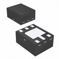
Extended Type Number ATR0610-PQQ Package PLLP6 Remarks Area 1.6 mm × 2.0 mm, 0.5 mm pitch, PB-free, RoHS compliant, green
9. Package Information
12
ATR0610
4573H–GPS–11/06
�ATR0610
13
4573H–GPS–11/06
�10. Revision History
Please note that the following page numbers referred to in this section refer to the specific revision mentioned, not to this document. Revision No. 4573H-GPS-11/06 History • Features on page 1 changed • Section 8 “Ordering Information” on page 12 changed • Put datasheet in a new template • ESD logo moved from page 1 to page 3 • Section 7 “Bill of Materials of Application Board” on page 11 changed
4573G-GPS-10/06
14
ATR0610
4573H–GPS–11/06
�Atmel Corporation
2325 Orchard Parkway San Jose, CA 95131, USA Tel: 1(408) 441-0311 Fax: 1(408) 487-2600
Atmel Operations
Memory
2325 Orchard Parkway San Jose, CA 95131, USA Tel: 1(408) 441-0311 Fax: 1(408) 436-4314
RF/Automotive
Theresienstrasse 2 Postfach 3535 74025 Heilbronn, Germany Tel: (49) 71-31-67-0 Fax: (49) 71-31-67-2340 1150 East Cheyenne Mtn. Blvd. Colorado Springs, CO 80906, USA Tel: 1(719) 576-3300 Fax: 1(719) 540-1759
Regional Headquarters
Europe
Atmel Sarl Route des Arsenaux 41 Case Postale 80 CH-1705 Fribourg Switzerland Tel: (41) 26-426-5555 Fax: (41) 26-426-5500
Microcontrollers
2325 Orchard Parkway San Jose, CA 95131, USA Tel: 1(408) 441-0311 Fax: 1(408) 436-4314 La Chantrerie BP 70602 44306 Nantes Cedex 3, France Tel: (33) 2-40-18-18-18 Fax: (33) 2-40-18-19-60
Biometrics/Imaging/Hi-Rel MPU/ High-Speed Converters/RF Datacom
Avenue de Rochepleine BP 123 38521 Saint-Egreve Cedex, France Tel: (33) 4-76-58-30-00 Fax: (33) 4-76-58-34-80
Asia
Room 1219 Chinachem Golden Plaza 77 Mody Road Tsimshatsui East Kowloon Hong Kong Tel: (852) 2721-9778 Fax: (852) 2722-1369
ASIC/ASSP/Smart Cards
Zone Industrielle 13106 Rousset Cedex, France Tel: (33) 4-42-53-60-00 Fax: (33) 4-42-53-60-01 1150 East Cheyenne Mtn. Blvd. Colorado Springs, CO 80906, USA Tel: 1(719) 576-3300 Fax: 1(719) 540-1759 Scottish Enterprise Technology Park Maxwell Building East Kilbride G75 0QR, Scotland Tel: (44) 1355-803-000 Fax: (44) 1355-242-743
Japan
9F, Tonetsu Shinkawa Bldg. 1-24-8 Shinkawa Chuo-ku, Tokyo 104-0033 Japan Tel: (81) 3-3523-3551 Fax: (81) 3-3523-7581
Literature Requests
www.atmel.com/literature
Disclaimer: T he information in this document is provided in connection with Atmel products. No license, express or implied, by estoppel or otherwise, to any intellectual property right is granted by this document or in connection with the sale of Atmel products. EXCEPT AS SET FORTH IN ATMEL’S TERMS AND CONDITIONS OF SALE LOCATED ON ATMEL’S WEB SITE, ATMEL ASSUMES NO LIABILITY WHATSOEVER AND DISCLAIMS ANY EXPRESS, IMPLIED OR STATUTORY WARRANTY RELATING TO ITS PRODUCTS INCLUDING, BUT NOT LIMITED TO, THE IMPLIED WARRANTY OF MERCHANTABILITY, FITNESS FOR A PARTICULAR PURPOSE, OR NON-INFRINGEMENT. IN NO EVENT SHALL ATMEL BE LIABLE FOR ANY DIRECT, INDIRECT, CONSEQUENTIAL, PUNITIVE, SPECIAL OR INCIDENTAL DAMAGES (INCLUDING, WITHOUT LIMITATION, DAMAGES FOR LOSS OF PROFITS, BUSINESS INTERRUPTION, OR LOSS OF INFORMATION) ARISING OUT OF THE USE OR INABILITY TO USE THIS DOCUMENT, EVEN IF ATMEL HAS BEEN ADVISED OF THE POSSIBILITY OF SUCH DAMAGES. A tmel makes no representations or warranties with respect to the accuracy or completeness of the contents of this document and reserves the right to make changes to specifications and product descriptions at any time without notice. Atmel does not make any commitment to update the information contained herein. Unless specifically provided otherwise, Atmel products are not suitable for, and shall not be used in, automotive applications. Atmel’s products are not intended, authorized, or warranted for use as components in applications intended to support or sustain life.
© 2006 Atmel Corporation. A ll rights reserved. A tmel ®, logo and combinations thereof, Everywhere You Are® a nd others are registered trademarks or trademarks of Atmel Corporation or its subsidiaries. Other terms and product names may be trademarks of others.
4573H–GPS–11/06
�