5962-8876904KPA

5962-8876904KPA

  • 厂商:

    AVAGO(博通)

  • 封装:

  • 描述:

    5962-8876904KPA - Hermetically Sealed Low IF, Wide VCC, Logic Gate Optocouplers - AVAGO TECHNOLOGIES...

  • 详情介绍
  • 数据手册
  • 价格&库存
5962-8876904KPA 数据手册
HCPL-520x, HCPL-523x, HCPL-623x, HCPL-625x, 5962-88768 and 5962-88769 Hermetically Sealed Low IF, Wide VCC, Logic Gate Optocouplers Data Sheet Description �he�e unit� are �ingle�� dual and quad channel�� hermeti� call�� �ealed o�tocou�ler�. �he �roduct� are ca�able o� o�eration and �torage over the �ull militar�� tem�erature range and can be �urcha�ed a� either �tandard �roduct or with �ull M���P��������� Cla�� �evel �� or � te�ting or �rom the a��ro�riate DSCC Drawing. �ll device� are manu�actured and te�ted on a M���P��������� certified line and are included in the DSCC �ualified Manu�actur� er� �i�t �M�������� �or ����brid Microcircuit�. Each channel contain� an �l�a�� light emitting diode which i� o�ticall�� cou�led to an integrated high gain �hoton detector. �he detector ha� a thre�hold with h���� tere�i� which �rovide� differential mode noi�e immunit�� and eliminate� the �otential �or out�ut �ignal chatter. �he detector in the �ingle channel unit� ha� a tri��tate out�ut �tage which allow� �or direct connection to data bu�e�. �he out�ut i� noninverting. �he detector �C ha� an internal �hield that �rovide� a guaranteed common mode tran�ient immunit�� o� u� to �0��000 ����. �m�roved �ower �u��l�� rejection eliminate� the need �or ��ecial �ower �u��l�� b���a�� �recaution�. Features • Dual Marked with Device Part Number and DSCC Standard Microcircuit Drawing • Manu�actured and �e�ted on a M���P��������� Certi� Manu�actured and �e�ted on a M���P��������� Certi� fied �ine • �M���������� Cla�� �� and � �M���������� Cla�� �� and � • �our ��ermeticall�� Sealed Package Configuration� �our ��ermeticall�� Sealed Package Configuration� • Per�ormance �uaranteed over ����C to �����C Per�ormance �uaranteed over ����C to �����C • �ide �CC �ange (��.� to �0 �) �ide � • ��0 n� Ma�imum Pro�agation Dela�� ��0 n� Ma�imum Pro�agation Dela�� • CM��� �� �0��000 ���� ����ical CM��� �� �0��000 ���� ����ical • ��00 �dc �ith�tand �e�t �oltage ��00 �dc �ith�tand �e�t �oltage • �hree State �ut�ut �vailable �hree State �ut�ut �vailable • ��igh �adiation �mmunit�� ��igh �adiation �mmunit�� • ��CP����00��� �unction Com�atibilit�� ��CP����00��� �unction Com�atibilit�� • �eliabilit�� Data �vailable �eliabilit�� Data �vailable • Com�atible with �S����� ����� and CM�S �ogic Com�atible with �S����� ����� and CM�S �ogic Applications • • • • • • • • • Militar�� and S�ace ��igh �eliabilit�� S���tem� �ran��ortation and �i�e Critical S���tem� ��igh S�eed �ine �eceiver ��olated Bu� Driver (Single Channel) Pul�e �ran��ormer �e�lacement �round �oo� Elimination ��ar�h �ndu�trial Environment� Com�uter�Peri�heral �nter�ace� Note�� � 0.� m� b���a�� ca�acitor mu�t be connected between �CC and �ND �in�. CAUTION: It is advised that normal static precautions be taken in handling and assembly of this component to prevent damage and/or degradation which may be induced by ESD. Functional Diagram Multi�le Channel Device� �vailable V CC VO Truth Tables (Po�itive �ogic) Multichannel Devices Input On (H) Off (L) Output H L VE GND Package �t��le� �or the�e �art� are � �in D�P through hole (ca�e outline P)�� �6 �in D�P flat �ack (ca�e outline �)�� and leadle�� ceramic chi� carrier (ca�e outline �). Device� ma�� be �urcha�ed with a variet�� o� lead bend and �lating o�tion��� �ee Selection �uide �able �or detail�. Standard Microcircuit Drawing (SMD) �art� are available �or each �ackage and lead �t��le. Becau�e the �ame electrical die (emitter� and detector�) are u�ed �or each channel o� each device li�ted in thi� data �heet�� ab�olute ma�imum rating��� recommended o�erating condition��� electrical ��ecification��� and �er�or� mance characteri�tic� �hown in the figure� are identical �or all �art�. �cca�ional e�ce�tion� e�i�t due to �ackage variation� and limitation� and are a� noted. �dditionall���� the �ame �ackage a��embl�� �roce��e� and material� are u�ed in all device�. �he�e �imilaritie� give ju�tification �or the u�e o� data obtained �rom one �art to re�re�ent other �art’� �er�ormance �or die related reliabilit�� and certain limited radiation te�t re�ult�. Single Channel Devices Input On (H) Off (L) On (H) Off (L) Enable H H L L Output Z Z H L Functional Diagrams 8 Pin DIP Through Hole 1 Channel 1 2 3 4 V CC VO 8 7 6 5 8 Pin DIP Through Hole 2 Channels 1 2 3 4 V CC V O1 V O2 8 7 6 5 1 2 3 4 5 6 7 8 16 Pin Flat Pack Unformed Leads 4 Channels 16 V CC V O1 V O2 V O3 V O4 GND 15 14 13 12 11 10 9 20 Pad LCCC Surface Mount 2 Channels 15 V CC2 19 20 V O2 GND 2 V O1 GND 1 7 8 V CC1 13 12 VE GND 2 3 10 GND Note�� Multichannel D�P and flat �ack device� have common �CC and ground. Single channel D�P ha� an enable �in 6. �CCC (leadle�� ceramic chi� carrier) �ackage ha� i�olated channel� with �e�arate �CC and ground connection�.  Selection Guide–Package Styles and Lead Configuration Options Package Lead Style Channels Common Channel Wiring Avago Technologies’ Part Numbers and Options Commercial MIL-PRF-38534 Class H MIL-PRF-38534 Class K Standard Lead Finish Solder Dipped* Butt Joint/Gold Plate Gull Wing/Soldered* Class H SMD Part Number Prescript for all below Either Gold or Soldered Gold Plate Solder Dipped* Butt Joint/Gold Plate Butt Joint/Soldered* Gull Wing/Soldered* Class K SMD Part Number Prescript for all below Either Gold or Soldered Gold Plate Solder Dipped* Butt Joint/Gold Plate Butt Joint/Soldered* Gull Wing/Soldered* * Solder contain� lead 8 Pin DIP Through Hole 1 None 8 Pin DIP Through Hole 2 VCC GND HCPL-5230 HCPL-5231 HCPL-523K Gold Plate Option 200 Option 100 Option 300 16 Pin Flat Pack Unformed Leads 4 VCC GND HCPL-6250 HCPL-6251 HCPL-625K Gold Plate 20 Pad LCCC Surface Mount 2 None HCPL-5200 HCPL-5201 HCPL-520K Gold Plate Option 200 Option 100 Option 300 HCPL-6230 HCPL-6231 HCPL-623K Solder Pads * 59628876801PX 8876801PC 8876801PA 8876801YC 8876801YA 8876801XA 59628876901PX 8876901PC 8876901PA 8876901YC 8876901YA 8876901XA 59628876903FX 8876903FC 596288769022X 88769022A 59628876802KPX 8876802KPC 8876802KPA 8876802KYC 8876802KYA 8876802KXA 59628876904KPX 8876904KPC 8876904KPA 8876904KYC 8876904KYA 8876904KXA 59628876906KFX 8876906KFC 59628876905K2X 8876905K2A  Outline Drawings 8 Pin DIP Through Hole, 1 and 2 Channel 9.40 (0.370) 9.91 (0.390) 0.76 (0.030) 1.27 (0.050) 4.32 (0.170) MAX. 0.51 (0.020) MIN. 8.13 (0.320) MAX. 7.16 (0.282) 7.57 (0.298) 3.81 (0.150) MIN. 0.20 (0.008) 0.33 (0.013) 7.36 (0.290) 7.87 (0.310) 2.29 (0.090) 2.79 (0.110) 0.51 (0.020) MAX. NOTE: DIMENSIONS IN MILLIMETERS (INCHES). 16 Pin Flat Pack, 4 Channels 7.24 (0.285) 6.99 (0.275) 2.29 (0.090) MAX. 1.27 (0.050) REF. 11.13 (0.438) 10.72 (0.422) 0.46 (0.018) 0.36 (0.014) 2.85 (0.112) MAX. 8.13 (0.320) MAX. 0.89 (0.035) 0.69 (0.027) 5.23 (0.206) MAX. 0.88 (0.0345) MIN. 9.02 (0.355) 8.76 (0.345) 0.31 (0.012) 0.23 (0.009) NOTE: DIMENSIONS IN MILLIMETERS (INCHES).  20 Terminal LCCC Surface Mount, 2 Channels 8.70 (0.342) 9.10 (0.358) 4.95 (0.195) 5.21 (0.205) 1.02 (0.040) (3 PLCS) 1.14 (0.045) 1.40 (0.055) 8.70 (0.342) 9.10 (0.358) 4.95 (0.195) 5.21 (0.205) 1.78 (0.070) 2.03 (0.080) 0.64 (0.025) (20 PLCS) 1.52 (0.060) 2.03 (0.080) NOTE: DIMENSIONS IN MILLIMETERS (INCHES). SOLDER THICKNESS 0.127 (0.005) MAX. 1.78 (0.070) 2.03 (0.080) TERMINAL 1 IDENTIFIER 2.16 (0.085) METALIZED CASTILLATIONS (20 PLCS) 0.51 (0.020) Leaded Device Marking AVAGO Designator AVAGO P/N DSCC SMD* DSCC SMD* PIN ONE/ ESD IDENT A QYYWWZ XXXXXX XXXXXXX XXX XXX 50434 COMPLIANCE INDICATOR,* DATE CODE, SUFFIX (IF NEEDED) COUNTRY OF MFR. AVAGO FSCN* *QUALIFIED PARTS ONLY Leadless Device Marking AVAGO Designator AVAGO P/N PIN ONE/ ESD IDENT COUNTRY OF MFR. A QYYWWZ XXXXXX XXXX XXXXXX XXX 50434 COMPLIANCE INDICATOR,* DATE CODE, SUFFIX (IF NEEDED) DSCC SMD* DSCC SMD* AVAGO FSCN* *QUALIFIED PARTS ONLY  Hermetic Optocoupler Options Option 100 Description Surface mountable hermetic optocoupler with leads trimmed for butt joint assembly. This option is available on commercial and hi-rel product in 8 pin DIP (see drawings below for details). 4.32 (0.170) MAX. 0.51 (0.020) MIN. 2.29 (0.090) 2.79 (0.110) 1.14 (0.045) 1.40 (0.055) 0.51 (0.020) MAX. NOTE: DIMENSIONS IN MILLIMETERS (INCHES). 0.20 (0.008) 0.33 (0.013) 7.36 (0.290) 7.87 (0.310) 200 Lead finish is solder dipped rather than gold plated. This option is available on commercial and hi-rel product in 8 pin DIP. DSCC Drawing part numbers contain provisions for lead finish. All leadless chip carrier devices are delivered with solder dipped terminals as a standard feature. Surface mountable hermetic optocoupler with leads cut and bent for gull wing assembly. This option is available on commercial and hi-rel product in 8 pin DIP (see drawings below for details). This option has solder dipped leads. 4.57 (0.180) MAX. 0.20 (0.008) 0.33 (0.013) 9.65 (0.380) 9.91 (0.390) 4.57 (0.180) MAX. 300 0.51 (0.020) MIN. 2.29 (0.090) 2.79 (0.110) 1.40 (0.055) 1.65 (0.065) 0.51 (0.020) MAX. 5˚ MAX. NOTE: DIMENSIONS IN MILLIMETERS (INCHES). Note: Solder contain� lead  Absolute Maximum Ratings Parameter Storage �em�erature �ange ��erating �mbient �em�erature Junction �em�erature Ca�e �em�erature �ead Solder �em�erature (�.6 mm below �eating �lane) �verage �orward Current�� each channel Peak �n�ut Current�� each channel �ever�e �n�ut �oltage�� each channel �verage �ut�ut Current�� each channel Su��l�� �oltage �ut�ut �oltage�� each channel Package Power Di��i�ation�� each channel �� ��� ��P� �� �� �CC �� PD 0.0 �0.� Symbol �S �� �J �C Min. �6�� ���� Max. ���0� ����� ��7�� ��70� �60� �or �0 � � �0 [�] � �� �0 �0 �00 Units C C C C C m� m� � m� � � m� Single Channel Product Only �ri�State Enable �oltage �E �0.� �0 � 8 Pin Ceramic DIP Single Channel Schematic Note enable �in 6. �n e�ternal 0.0� �� to 0.� �� b���a�� ca�acitor i� recommended between �CC and ground �or each �ackage t���e. ESD Classification (MIL-STD-883, Method 3015) ��CP����00�0��0� and ��CP��6��0������ ��CP�����0������ and ��CP��6��0������ (D)�� Cla�� � (Dot)�� Cla�� � Recommended Operating Conditions Parameter Power Su��l�� �oltage �n�ut Current�� ��igh �evel�� each channel �n�ut �oltage�� �ow �evel�� each channel �an �ut (��� �oad)�� each channel Symbol �CC ���� ��� N Min. ��.� � 0 Max. �0 � 0.� �� Units � m� � Single Channel Product Only ��igh �evel Enable �oltage �ow �evel Enable �oltage �E�� �E� �.0 0 �0 0.� � �  Electrical Characteristics �� = ����C to �����C�� ��.� � ≤ �CC ≤ �0 ��� � m� ≤ ��(�N) ≤ � m��� 0 � ≤ ��(���) ≤ 0.� ��� unle�� otherwi�e ��ecified. Parameter �ogic �ow �ut�ut �oltage �ogic ��igh �ut�ut �oltage Symbol ��� ���� Group A, Sub-groups[11] ��� ��� � ��� ��� � N� �ut�ut �eakage Current (��U� �� �CC) ������ ��� ��� � Limits Test Conditions ��� = 6.�� m� (�� ��� �oad�) ���� = ��.6 m��� (**���� = �CC � �.� �) ���� = �0.�� m� �� = �.� � �� = �0 � �ogic �ow Su��l�� Current Single Channel �CC� ��� ��� � �CC = �.� � �CC = �0 � �CC = �.� � �CC = �0 � �CC = �.� � �CC = �0 � �CC�� ��� ��� � �CC = �.� � �CC = �0 � �CC = �.� � �CC = �0 � �CC = �.� � �CC = �0 � ��S� ��� ��� � �� = �CC = �.� � �� = �CC = �0 � �ogic ��igh Short Circuit �ut�ut Current �n�ut �orward �oltage �n�ut �ever�e Breakdown �oltage �n�ut��ut�ut �n�ulation �eakage Current �ogic ��igh Common Mode �ran�ient �mmunit�� �ogic �ow Common Mode �ran�ient �mmunit�� Pro�agation Dela�� �ime to �ogic �ow Pro�agation Dela�� �ime to �ogic ��igh ��S�� �� B�� ���� ��� ��� � �CC = �.�� �CC = �0 � ��� ��� � ��� ��� � � �� = � m� �� = �ND �.0 � �.0 �.� �� = � m� �CC = ��.� � �� = 0 � �E = Don’t Care ��� = ��� = 0 � ��� = ��� = ��� = ���� =0 � �� = �m� �E = Don’t Care ��� = ��� = �m� ��� = ��� = ��� = ���� = �m� �� = 0 � �0 �� ��0 ��� �.� � � m� �� � � ���� � m� ��� � ��.� �.� 9.0 �0.6 ��� �7 �.9 �.� �.� 6.6 9 �� �.�� ** �.� �00 �00 6 7.� �� �� ��� �0 ��.� 6 9 �� �� ��� m� ��� � m� m� m� � Min. Typ.* Max. 0.� Units � � Fig. ��� � ��� � Notes � � Dual Channel �uad Channel �ogic ��igh Su��l�� Current Single Channel Dual Channel �uad Channel �ogic �ow Short Circuit �ut�ut Current �� = � m� �� = �0 m� ���� = ��00 �dc�� t = ���� ��� ≤ 6�%�� �� = ���C �� = � m��� �CM = �0 �P�P �� = 0 m��� �CM = �0 �P�P |CM��| |CM�| tP��� tP��� 9�� �0�� �� 9�� �0�� �� 9�� �0�� �� 9�� �0�� �� �000 �0��000 �000 �0��000 �7� ��� ��0 ��0 ��m� ��m� n� n� 9 9 ��� 6 ��� 6 ��� 6�� �� ��� 6�� �� ��� 7 ��� 7  Electrical Characteristics - Single Channel Product Only �� = ����C to �����C�� ��.� � ≤ �CC ≤ �0 ��� � m� ≤ �� (�N) ≤ � m��� 0 � ≤ ��(���) ≤ 0.� ��� �.0 � ≤ �E�� ≤ �0 ��� 0 � ≤ �E� ≤ 0.� ��� unle�� otherwi�e ��ecified. Parameter ��igh �m�edance State �ut�ut Current Symbol ��Z� ��Z�� Group A, Sub-groups[11] ������� ������� Limits Test Conditions �� = 0.�� � �� = �.�� � �� = �.� � �� = �0 � �EN = � ��� �� = 0 � �EN = � ��� �� = � m� Min. Typ.* Max. ��0 �0 �00 �00 Units m� m� Fig. Notes �ogic ��igh Enable �oltage �ogic �ow Enable �oltage �ogic ��igh Enable Current �E�� �E� �E�� ��� ��� � ��� ��� � ��� ��� � �EN = �.7 � �EN = �.� � �EN = �0 � �.0 0.� �0 �00 0.00�� ��0 �0.�� � � m� �ogic �ow Enable Current �E� ��� ��� � �EN = 0.�� � m� *�ll t���ical value� are at �CC = � ��� �� = ���C�� ��(�N) = � m� unle�� otherwi�e ��ecified.  Typical Characteristics �ll t���ical value� are at �� = ���C�� �CC = � ��� ��(�N) = � m� unle�� otherwi�e ��ecified. Parameter �n�ut Current �����tere�i� �n�ut Diode �em�erature Coefficient �e�i�tance (�n�ut��ut�ut) Ca�acitance (�n�ut��ut�ut) �n�ut Ca�acitance �ut�ut �i�e �ime (�0�90%) �ut�ut �all �ime (90��0%) Symbol ���YS D�� D�� ���� C��� C�N tr t� Test Conditions �CC = � � �� = � m� ���� = �00 �dc � = � M��z �� = 0 ��� � = � M��z Typ. 0.07 ��.�� �0�� �.0 �0 ��� �0 Units m� m���C W �� �� n� n� Fig. � Notes � � ��� � ��� � ��� �0 ��� 7 ��� 7 � � Single Channel Product Only �ut�ut Enable �ime to �ogic ��igh �ut�ut Enable �ime to �ogic �ow �ut�ut Di�able �ime �rom �ogic ��igh �ut�ut Di�able �ime �rom �ogic �ow tPZ�� tPZ� tP��Z tP�Z �0 �0 ��� �� n� n� n� n� � � � � Multi-Channel Product Only �n�ut��n�ut �n�ulation �eakage Current �e�i�tance (�n�ut��n�ut) Ca�acitance (�n�ut��n�ut) ���� ���� C��� ��� ≤ 6�%�� ���� = �00 ��� t = � � ���� = �00 � � = � M��z 0.� �0�� �.� n� W �� 9 9 9 Note��� �. Peak �orward �n�ut Current �ul�e width < �0 �� at � ���z ma�imum re�etition rate. �. Each channel o� a multichannel device. �. Duration o� out�ut �hort circuit time not to e�ceed �0 m�. ��. �ll device� are con�idered two�terminal device��� mea�ured between all in�ut lead� or terminal� �horted together and all out�ut lead� or ter� minal� �horted together. �. �hi� i� a momentar�� with�tand te�t�� not an o�erating condition. 6. CM� i� the ma�imum rate o� ri�e o� the common mode voltage that can be �u�tained with the out�ut voltage in the logic low �tate (�� < 0.� �). CM�� i� the ma�imum rate o� �all o� the common mode voltage that can be �u�tained with the out�ut voltage in the logic high �tate (�� �� �.0 �). 7. tP��� �ro�agation dela�� i� mea�ured �rom the �0% �oint on the leading edge o� the in�ut �ul�e to the �.� � �oint on the leading edge o� the out�ut �ul�e. �he tP��� �ro�agation dela�� i� mea�ured �rom the �0% �oint on the trailing edge o� the in�ut �ul�e to the �.� � �oint on the trailing edge o� the out�ut �ul�e. �. Mea�ured between each in�ut �air �horted together and all out�ut connection� �or that channel �horted together. 9. Mea�ured between adjacent in�ut �air� �horted together �or each multichannel device. �0. Zero�bia� ca�acitance mea�ured between the �ED anode and cathode. ��. Standard �art� receive �00% te�ting at ���C (Subgrou�� � and 9). SMD�� Cla�� �� and Cla�� � �art� receive �00% te�ting at ���� ����� and –���C (Subgrou�� � and 9�� � and �0�� � and ���� re��ectivel��). ��. Parameter� are te�ted a� �art o� device initial characterization and a�ter de�ign and �roce�� change�. Parameter� guaranteed to limit� ��eci� fied �or all lot� not ��ecificall�� te�ted. 10 Figure 1. Typical Logic Low Output Voltage vs. Temperature. Figure 2. Typical Logic High Output Current vs. Temperature. Figure 3. Output Voltage vs. Forward Input Current. Figure 4. Typical Diode Input Forward Characteristic. V CC PULSE GEN. t r = t f = 5 ns t = 100 kHz 10 % DUTY CYCLE INPUT MONITORING NODE Rf IF OUTPUT VO MONITORING NODE V CC VO CL= 15 pF 5K D1 D.U.T. 5V 619 Ω VE GND D2 D3 D4 THE PROBE AND JIG CAPACITANCES ARE INCLUDED IN C L . Figure 5. Test Circuit for tPLH, tPHL, tr, and tf. 11 Figure 6. Typical Propagation Delay vs. Temperature. Figure 7. Typical Rise, Fall Time vs. Temperature. PULSE GENERATOR Z O = 50 Ω t r = t f = 5 ns C L = 15 pF INCLUDING PROBE AND JIG CAPACITANCE. V CC D.U.T. V CC VO D1 +5 V S1 619 Ω IF VO CL VE GND INPUT VO MONITORING NODE D2 5 KΩ D3 D4 S2 Figure 8. Test Circuit for tPHZ, tPZH, tPLZ, and tPZL. A D.U.T. B R IN VCC VO VCC OUTPUT VO MONITORING NODE V FF VE GND 0.1 µF BYPASS V CM + PULSE GEN. Figure 9. Test Circuit for Common Mode Transient Immunity and Typical Waveforms. 1 V CC1 (+5 V) 665 Ω D.U.T. VCC DATA INPUT VO TTL OR LSTTL VE GND TOTEM POLE OUTPUT GATE V CC2 5V 10 V 15 V 20 V RL 1.1 K 2.37 K 3.83 K 5.11 K RL V CC2 (4.5 TO 20 V) V CC1 (+5 V) 750 Ω D.U.T. V CC DATA INPUT TOTEM POLE OUTPUT GATE TTL OR LSTTL CMOS DATA OUTPUT GND 1 2 Figure 10. LSTTL to CMOS Interface Circuit. Figure 11. Recommended LED Drive Circuit. V CC1 (+5 V) 619 Ω D.U.T. V CC 4.02 KΩ DATA INPUT TTL OR LSTTL GND OPEN COLLECTOR GATE Figure 12. Series LED Drive with Open Collector Gate (4.02 kΩ Resistor Shunts IOH from the LED). V CC2 (+5 V) DATA OUTPUT V CC1 (+5 V) 665 Ω 665 Ω D.U.T. V CC DATA INPUT TOTEM POLE OUTPUT GATE TTL OR LSTTL UP TO 16 LSTTL LOADS OR 4 TTL LOADS 0.1 µF DATA OUTPUT DATA INPUT 1 TOTEM POLE OUTPUT GATE TTL OR LSTTL GND UP TO 16 LSTTL LOADS OR 4 TTL LOADS 1 Figure 13. Recommended LSTTL to LSTTL Circuit. 2 V CC + 20 V D.U.T.* IF +V IN 1.90 V 100 Ω V CC IO VE GND 1200 Ω 0.01 µF MIL-PRF-38534 Class H, Class K, and DSCC SMD Test Program �vago �echnologie�’ ��i��el ��tocou�ler� are in com� �liance with M���P��������� Cla��e� �� and �. Cla�� �� and Cla�� � device� are al�o in com�liance with DSCC drawing� �96����76� and �96����769. �e�ting con�i�t� o� �00% �creening and qualit�� con�or� mance in��ection to M���P���������. CONDITIONS: I F = 8 mA IO = -14 mA T A = +125 ˚C *ALL CHANNELS TESTED SIMULTANEOUSLY. Figure 14. Single Channel Operating Circuit for Burn-in and Steady State Life Tests. For product information and a complete list of distributors, please go to our web site: www.avagotech.com Avago, Avago Technologies, and the A logo are trademarks of Avago Technologies, Limited in the United States and other countries. Data subject to change. Copyright © 2006 Avago Technologies Limited. All rights reserved. 5989-2666EN - April 4, 2007
5962-8876904KPA
1. 物料型号: - HCPL-520x, HCPL-523x, HCPL-623x, HCPL-625x, 5962-88768 和 5962-88769

2. 器件简介: - 这些是单通道、双通道和四通道的密封光耦器件。产品能够在全军用温度范围内操作和存储,并且可以作为标准产品或带有完整的MIL-PRF-38534 H级或K级测试购买,或来自适当的DSCC图纸。所有设备都在MIL-PRF-38534认证线上制造和测试,并包含在DSCC合格制造商名单QML-38534中,用于混合微电路。
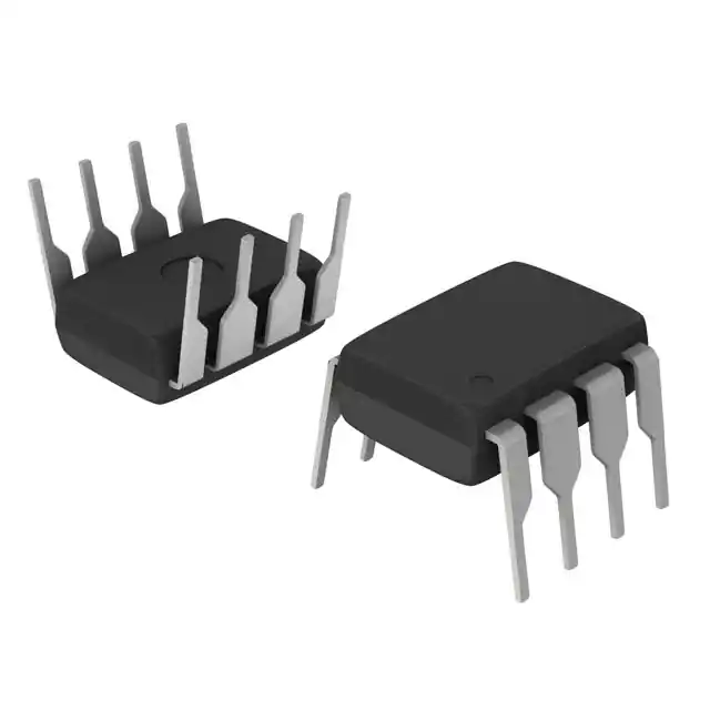
3. 引脚分配: - 8引脚DIP:Vcc、通道1、通道2、...、GND - 16引脚扁平包装:Vcc、通道1-4、GND - 20端LCCC:Vcc1、通道1-2、GND、Vcc2、通道3-4、GND

4. 参数特性: - 工作温度范围:-55°C至+125°C - 供电电压范围:4.5至20V - 最大传播延迟:350ns - 共模抑制比:>10,000V/us - 耐压测试电压:1500Vdc - 三态输出可用

5. 功能详解: - 每个通道包含一个AlGaAs发光二极管,与集成的高增益光子探测器光耦合。探测器具有带有滞后的阈值,提供差分模式噪声抑制,并消除输出信号抖动的潜力。单通道单元中的探测器具有三态输出级,允许直接连接到数据总线。输出为非反相。探测器IC内部有屏蔽,提供高达10,000V/us的共模瞬态免疫。

6. 应用信息: - 军事和航天、高可靠性系统、交通和生命关键系统、高速线接收器、隔离总线驱动器(单通道)、脉冲变压器替代、接地回路消除、恶劣工业环境、计算机外设接口。

7. 封装信息: - 8引脚DIP直插式封装、16引脚DIP扁平封装、无引线陶瓷芯片载体封装。设备可以购买各种引脚弯曲和电镀选项,详见选择指南表。每种封装和引脚样式都有标准微电路绘图(SMD)部件。
5962-8876904KPA 价格&库存

很抱歉,暂时无法提供与“5962-8876904KPA”相匹配的价格&库存,您可以联系我们找货

免费人工找货