Data Sheet
ACML-7400, ACML-7410, and ACML-7420
3.3V/5V 100-MBd High-Speed CMOS Digital
Isolator
Description
The Broadcom® ACML-7400, ACML-7410, and ACML7420 are multi-channel, high-speed CMOS digital isolators.
Using magnetic coupling through a thick insulation barrier,
the isolators enable high speed transmissions without
compromise in isolation performance. These isolators
consume low power even at high data rates, yet provide
excellent transient immunity performance in compact
surface-mount packages. The devices are qualified to a
maximum propagation delay of 36 ns and a maximum pulse
width distortion of 3 ns. They are capable of running at a 100
MBaud data rate.
Features
UL Recognised
ACML-7400, ACML-7410 ,and ACML-7420 are available in
16-pin SOIC wide-body packages. They operate at dual
3.3V/5V supply voltages. The DC and timing specifications
are specified over the temperature range of –40°C to
+105°C. ACML-7400, ACML-7410, and ACML-7420 are
built using CMOS input buff ers and CMOS output drivers to
eliminate the need for both input limiters and output pull-up
resistors. Refresh circuitry is built in to ensure DCcorrectness.
– 5600 VRMS for 1 min. per UL1577
– CSA Component Acceptance Notice #5
IEC 60950-1
– Basic Insulation, 800 VRMS max. working voltage
– Reinforced Insulation, 400 VRMS max. working
voltage
IEC 61010-1
– Basic Insulation, 800 VRMS max. working voltage
– Reinforced Insulation, 400 VRMS max. working
voltage
Applications
Isolated data interfaces
Data acquisition
Digital oscilloscopes
Power meters
High speed video transmission
Dual supply voltage compatible – 3.3V and 5V
Wide operating temperature range (-40° C to +105° C)
Support high speed data rate of at least 100 MBd
Lower power consumption – 15 mA per channel typical
Low propagation delay: 36 ns max.
Low propagation delay skew
– Channel-to-channel: 4 ns max.
– Part-to-part: 8 ns max.
Low pulse width distortion: 3 ns max.
Safety and regulatory approvals
IEC 60601-1
– Two means of patient protection, 250 VRMS max.
working voltage
– Two means of operator protectioin, 400 VRMS max.
working voltage
High common mode transient immunity: 75 kV/µs min.
CMOS buffer input and output
DC correctness
Lead-free
CAUTION! It is advised that normal static precautions be taken in handling and assembly of this component to prevent
damage and/or degradation that may be induced by ESD. The components featured in this data sheet are not
to be used in military or aerospace applications or environments.
Broadcom
AV02-2675EN
January 23, 2018
�ACML-7400, ACML-7410, and ACML-7420 Data Sheet
3.3V/5V 100-MBd High-Speed CMOS Digital Isolator
Device Selection Guide
Device Number
Channel Configuration
Package
ACML-7400
Quad, All-in-One
16-pin Small Outline, Wide Body
ACML-7410
Quad, Bi-directional, 3/1
16-pin Small Outline, Wide Body
ACML-7420
Quad, Bi-directional, 2/2
16-pin Small Outline, Wide Body
Ordering Information
ACML-7400, ACML-7410, and ACML-7420 are UL Recognized with 5600 VRMS for 1 minute per UL1577.
Option
Part Number
RoHS Compliant
Package
Surface Mount
-000E
Wide Body SO-16
X
ACML-7400
ACML-7410
ACML-7420
-500E
Tape and Reel
X
UL 5600 VRMS/ 1
Minute rating
X
Quantity
X
45 per tube
X
850 per reel
To order, choose a part number from the part number column and combine with the desired option from the option column
to form an order entry.
Example 1:
ACML-7420-500E to order product of Wide Body SO-16 package in Tape and Reel in RoHS compliant.
Functional Diagram
Quad Channel
ACML-7410
ACML-7400
ACML-7420
VDD2
VDD1
11
16
VDD2
VDD1
1
16
VDD2
GND1
22
15
15
GND2
GND1
22
15
GND2
GND1
2
15
GND2
VIN1
33
14
14
VO1
VIN1
33
14
VO1
VIN1
3
14
VO1
VIN2
44
13
13
VO2
VIN2
44
13
VO2
VIN2
4
13
VO2
VIN3
55
12
12
VO3
VIN3
55
12
VO3
VO3
5
12
VIN3
VIN4
66
11
11
VO4
VO4
66
11
VIN4
VO4
6
11
VIN4
NC
77
10
10
VOE2
VOE1
77
10
VOE2
VOE1
7
10
VOE2
GND1
88
99
GND2
GND1
88
9
GND2
GND1
8
9
GND2
Broadcom
Galvanic Isolation
16
16
Galvanic Isolation
Galvanic
Isolation
11
Galvanic Isolation
Galvanic
Isolation
VDD1
AV02-2675EN
2
�ACML-7400, ACML-7410, and ACML-7420 Data Sheet
3.3V/5V 100-MBd High-Speed CMOS Digital Isolator
Pin Description
Pin
Description
VDD1, VDD2
Power supply at primary and secondary side
GND1, GND2
Ground at primary and secondary side
VIN1, VIN2, VIN3, VIN4 Input for channel 1, 2, 3, and 4
VO1, VO2, VO3, VO4
Output for channel 1, 2, 3, and 4
VOE1, VOE2
Output enable at VDD1 and VDD2 side, these pins should be connected to the respective VDD when not in use.
NC
No connectivity
Truth Table (ACML-7410)
VDD1
VIN1,IN2,IN3
VOE1
VO4
VDD2
VIN4
VOE2
VO1, O2, O3
H
H
X
X
H
X
H or NC
H
Input (VIN1, IN2, IN3) logic High during normal
operation. The enable (VOE2) default state is High.
H
L
X
X
H
X
H or NC
L
Input (VIN1, IN2, IN3) logic Low during normal operation.
The enable (VOE2) default state is High.
H
X
X
X
H
X
L
Z
Output (VO1, O2, O3) is disabled to high impedance
state when VOE2 is set to Low.
L
X
X
X
H
X
H
H
When VDD1 is not powered, the output (VO1, O2, O3)
default state is High. Output (VO1, O2, O3) typically
restored 100 µs after VDD1 is restored.
H
X
H or NC
H
H
H
X
X
Input (VIN4) logic High during normal operation. The
enable (VOE1) default state is High.
H
X
H or NC
L
H
L
X
X
Input (VIN4) logic Low during normal operation. The
enable (VOE1) default state is High.
H
X
L
Z
H
X
X
X
Output (VO4) is disabled to high impedance state
when VOE1 is set to Low.
H
X
H
H
L
X
X
X
When VDD2 is not powered, the output (VO4) default
state is High. Output (VO4) typically restored 100 ms
after VDD2 is restored.
Broadcom
Remark
AV02-2675EN
3
�ACML-7400, ACML-7410, and ACML-7420 Data Sheet
3.3V/5V 100-MBd High-Speed CMOS Digital Isolator
Package Outline Drawings
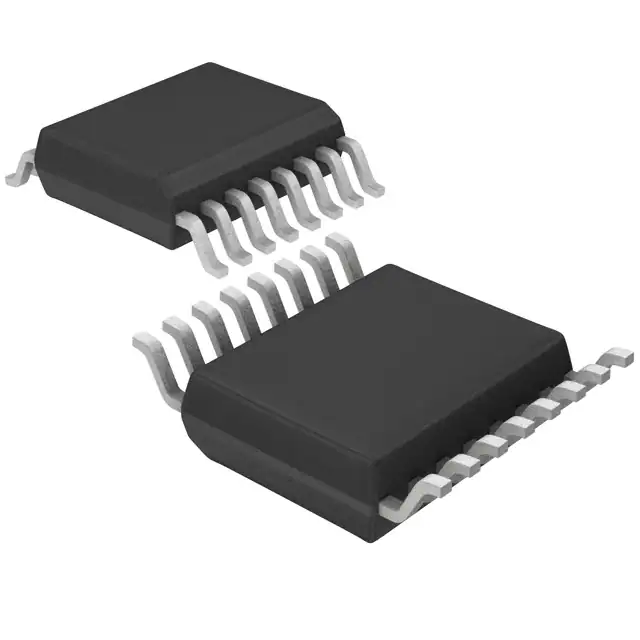
ACML-7400, ACML-7410 and ACML-7420 16-Lead Surface Mount (SOIC-16) Package
0.457
(0.018)
LAND PATTERN RECOMMENDATION
0.64 (0.025)
1.270
(0.050)
16 15 14 13 12 11 10 9
TYPE NUMBER
DATE CODE
A 7400
YYWW
EEE
7.493 ± 0.254
(0.295 ± 0.010)
11.63 (0.458)
2.16 (0.085)
LOT ID
1 2 3 4 5 6 7 8
10.312 ± 0.254
(0.406 ± 0.10)
0.457
(0.018)
ALL LEADS
TO BE
COPLANAR
± 0.002
8.986 ± 0.254
(0.345 ± 0.010)
9°
3.505 ± 0.127
(0.138 ± 0.005)
0-8°
0.025 MIN.
10.160 ± 0.254
(0.408 ± 0.010)
0.203 ± 0.076
(0.008 ± 0.003)
STANDOFF
DIMENSIONS IN MILLIMETERS AND (INCHES).
NOTE: FLOATING LEAD PROTRUSION IS 0.15 mm (6 mils) MAX.
Recommended Pb-Free IR Profile
Recommended reflow condition as per JEDEC Standard, J-STD-020 (latest revision). Non-halide flux should be used.
Regulatory Information
The ACML-7400, ACML-7410 and ACML-7420 are approved by the following organizations.
UL
UL1577, component recognition program.
CSA
CSA Component Acceptance Service Notice #5A.
TUV RheInland
IEC 60950-1
Insulation
Category
Reinforced
Working Voltage 400 VRMS
(567 VPEAK)
Broadcom
Basic
IEC 61010-1
Reinforced
Basic
IEC 60601-1
2 Means of Patient 2 Means of Operator
Protection
Protection
800 VRMS
400 VRMS
800 VRMS
250 VRMS
400 VRMS
(1132 VPEAK)
(567 VPEAK)
(1132 VPEAK)
(354 VPEAK)
(567 VPEAK)
AV02-2675EN
4
�ACML-7400, ACML-7410, and ACML-7420 Data Sheet
3.3V/5V 100-MBd High-Speed CMOS Digital Isolator
Insulation and Safety-Related Specifications
Symbol
ACML-7400
ACML-7410
ACML-7420
Units
Minimum External Air Gap
(Clearance)
L(101)
8.1
mm
Measured from input terminals to output terminals,
shortest distance through air.
Minimum External Tracking
(Creepage)
L(102)
8.1
mm
Measured from input terminals to output terminals,
shortest distance path along body.
0.05
mm
Through insulation distance conductor to conductor,
usually the straight line distance thickness between
the emitter and detector.
>175
V
Parameter
Minimum Internal Plastic Gap
(Internal Clearance)
Tracking Resistance (Comparative
Tracking Index)
CTI
Isolation Group
IIIa
Conditions
DIN IEC 112/VDE 0303 Part 1
Material Group (DIN VDE 0110, 1/89, Table 1)
All creepage and clearance pertain to the isolation component itself. These dimensions are needed as a starting point for
the designer when determining the circuit insulation requirements, and not reflective of the equipment standard
requirements.
NOTE:
These isolators are suitable for safe electrical isolation only within the safety limit data. Maintenance of the safety
data shall be ensured by means of protective circuits.
Absolute Maximum Ratings
Parameter
Symbol
Min.
Max.
Units
Storage Temperature
TS
–55
+125
°C
Ambient Operating Temperature
TA
–40
+125
°C
Supply Voltages
VDD1, VDD2
0
6.5
Volts
Input Voltage
VI
–0.5
VDD +0.5
Volts
Output Voltage
VO
–0.5
VDD +0.5
Volts
Average Output Current
IO
—
±15
mA
Human Body Model
HBM
—
±4
kV
Charge Device Model
CDM
—
±1
kV
Electrostatic Discharge
Solder Reflow Temperature Profile
See the Solder Reflow Temperature Profile
Recommended Operating Conditions
Parameter
Symbol
Min.
Max.
Units
TA
–40
+105
°C
Supply Voltages ( 3.3V operation)
VDD1, VDD2
3.0
3.6
V
Supply Voltages (5V operation)
Ambient Operating Temperature
VDD1, VDD2
4.5
5.5
V
Logic High Input Voltage
VIH
0.7 × VDD
VDD
V
Logic Low Input Voltage
VIL
0.0
0.3 × VDD
V
Broadcom
Notes
AV02-2675EN
5
�ACML-7400, ACML-7410, and ACML-7420 Data Sheet
3.3V/5V 100-MBd High-Speed CMOS Digital Isolator
Electrical Specifications
ACML-7400
The following specifications apply to ACML-7400 and are applicable to ambient temperature of –40°C ≤ TA ≤ 105°C, input
supply of 3.0V ≤ VDD1 ≤ 3.6V or 4.5V ≤ VDD1 ≤ 5.5V, and output supply of 3.0V ≤ VDD2 ≤ 3.6 V or 4.5V ≤ VDD2 ≤ 5.5V. All
typical specifications at TA = +25°C.
Parameter
Symbol
Min.
Typ.
Max.
Unit
Test Conditions
Input Supply Current,
No data
IDD1(0)
—
5.9a
10
mA
Input Supply Current,
25 MBd data rate
IDD1(25)
Input Supply Current,
100 MBd data rate
IDD1(100)
16
—
mA
17
—
—
Output Supply
Current, No data
IDD2(0)
Output Supply
Current, 25 MBd
IDD2(25)
—
Output Supply
Current, 100 MBd
data rate
IDD2(100)
—
VDD1 = 3.3V
VDD1 = 5.0V
30a
40
31c
40
12a
16
mA
VDD1 = 3.6V
VDD1 = 5.5V
mA
No Input
1, 7
b
12.5-MHz logic
signal
1, 7
d
50-MHz logic
signal
1, 7
d
No Input
2, 8
e
12.5-MHz logic
signal
2, 8
f
50-MHz logic
signal
2, 8
f
VDD1 = 5.5V
13c
15
Notes
VDD1 = 5.5V
6.8c
—
Figure
—
mA
VDD1 = 3.3V
a
23
32
mA
VDD1 = 3.6V
30c
40
17
VDD1 = 5.0V
VDD1 = 5.5V
Logic Input Current
IIN
–10
—
10
µA
Logic High Output
Voltage
VOH
VDD – 0.1
VDD – 0.02
—
V
IOUT = –20 µA, VIN = VDD1
0.8 × VDD
VDD – 0.25
—
V
IOUT = –4 mA, VIN = VDD1
Logic Low Output
Voltage
VOL
–
0.02
0.1
V
IOUT = 20 µA, VIN = 0V
0.25
0.8
V
IOUT = 4 mA, VIN = 0V
a. Typical data based on 3.3V supply.
b. IDD1(0) is the supply current consumption at VDD1 when there is no signal to all inputs.
c. Typical data based on 5.0V supply.
d. IDD1(F) is the supply current consumption at VDD1 when inputs are switching at the specified data rate, and outputs are switching at same data
rate with no load.
e. IDD2(0) is the supply current consumption at VDD2 when there is no signal to all inputs.
f. IDD2(F) is the supply current consumption at VDD2 when inputs are switching at the specified data rate, and outputs are switching at same
data rate with no load.
Broadcom
AV02-2675EN
6
�ACML-7400, ACML-7410, and ACML-7420 Data Sheet
3.3V/5V 100-MBd High-Speed CMOS Digital Isolator
ACML-7410
The following specifications apply to ACML-7410 and are applicable to ambient temperature of –40°C ≤ TA ≤ 105°C, input
supply of 3.0V ≤ VDD1 ≤ 3.6V or 4.5V ≤ VDD1 ≤ 5.5V, and output supply of 3.0V ≤ VDD2 ≤ 3.6 V or 4.5V ≤ VDD2 ≤ 5.5V. All
typical specifications at TA = +25°C.
Parameter
Symbol
Min.
Typ.
Max.
Unit
Test Conditions
Input Supply Current,
No data
IDD1(0)
—
8.4a
11.5
mA
Input Supply Current,
25 MBd data rate
IDD1(25)
Input Supply Current,
100 MBd data rate
IDD1(100)
Output Supply
Current, No data
IDD2(0)
Output Supply
Current, 25 MBd
IDD2(25)
Output Supply
Current, 100 MBd
data rate
IDD2(100)
—
—
—
—
15.5a
—
17c
—
28.5a
40
30.5c
40
9.5
a
Notes
No Input
3, 7
b
12.5-MHz logic
signal
3, 7
d
50-MHz logic
signal
3, 7
d
No Input
4, 8
e
12.5-MHz logic
signal
4, 8
f
50-MHz logic
signal
4, 8
f
VDD1 = 5.5V
9.4c
—
Figure
16
10.4c
—
15a
—
17c
—
25a
34
30c
40
mA
VDD1 = 3.3V
VDD1 = 5.0V
mA
VDD1 = 3.6V
VDD1 = 5.5V
mA
VDD1 = 5.5V
mA
VDD1 = 3.3V
VDD1 = 5.0V
mA
VDD1 = 3.6V
VDD1 = 5.5V
Logic Input Current
IIN
–10
—
10
µA
Logic High Output
Voltage
VOH
VDD – 0.1
VDD – 0.02
—
V
IOUT = –20 µA, VIN = VDD1
0.8 × VDD
VDD – 0.25
—
V
IOUT = –4 mA, VIN = VDD1
Logic Low Output
Voltage
VOL
–
0.02
0.1
V
IOUT = 20 µA, VIN = 0V
0.25
0.8
V
IOUT = 4 mA, VIN = 0V
a. Typical data based on 3.3V supply.
b. IDD1(0) is the supply current consumption at VDD1 when there is no signal to all inputs.
c. Typical data based on 5.0V supply.
d. IDD1(F) is the supply current consumption at VDD1 when inputs are switching at the specified data rate, and outputs are switching at same data
rate with no load.
e. IDD2(0) is the supply current consumption at VDD2 when there is no signal to all inputs.
f. IDD2(F) is the supply current consumption at VDD2 when inputs are switching at the specified data rate, and outputs are switching at same data
rate with no load.
Broadcom
AV02-2675EN
7
�ACML-7400, ACML-7410, and ACML-7420 Data Sheet
3.3V/5V 100-MBd High-Speed CMOS Digital Isolator
ACML-7420
The following specifications apply to ACML-7420 and are applicable to ambient temperature of –40°C ≤ TA ≤ 105°C, input
supply of 3.0V ≤ VDD1 ≤ 3.6V or 4.5V ≤ VDD1 ≤ 5.5V, and output supply of 3.0V ≤ VDD2 ≤ 3.6 V or 4.5V ≤ VDD2 ≤ 5.5V. All
typical specifications at TA = +25°C.
Parameter
Symbol
Min.
Typ.
Max.
Unit
Test Conditions
Input Supply Current,
No data
IDD1(0)
—
9.0a
13
mA
Input Supply Current,
25 MBd data rate
IDD1(25)
Input Supply Current,
100 MBd data rate
IDD1(100)
15a
—
mA
Output Supply
Current, No data
IDD2(0)
Output Supply
Current, 25 MBd
IDD2(25)
Output Supply
Current, 100 MBd
data rate
IDD2(100)
—
27a
36
30c
40
a
13
9.0
mA
15a
mA
No Input
5, 7
b
12.5-MHz logic
signal
5, 7
d
50-MHz logic
signal
5, 7
d
No Input
6, 8
e
12.5-MHz logic
signal
6, 8
f
50-MHz logic
signal
6, 8
f
VDD1 = 5.5V
—
mA
VDD1 = 3.3V
VDD1 = 5.0V
17c
—
VDD1 = 3.6V
VDD1 = 5.5V
9.9c
—
VDD1 = 3.3V
VDD1 = 5.0V
17c
—
Notes
VDD1 = 5.5V
9.9c
—
Figure
27a
36
30c
40
mA
VDD1 = 3.6V
VDD1 = 5.5V
Logic Input Current
IIN
–10
—
10
µA
Logic High Output
Voltage
VOH
VDD – 0.1
VDD – 0.02
—
V
IOUT = –20 µA, VIN = VDD1
0.8 × VDD
VDD – 0.25
—
V
IOUT = –4 mA, VIN = VDD1
Logic Low Output
Voltage
VOL
–
0.02
0.1
V
IOUT = 20 µA, VIN = 0V
0.25
0.8
V
IOUT = 4 mA, VIN = 0V
a. Typical data based on 3.3V supply.
b. IDD1(0) is the supply current consumption at VDD1 when there is no signal to all inputs.
c. Typical data based on 5.0V supply.
d. IDD1(F) is the supply current consumption at VDD1 when inputs are switching at the specified data rate, and outputs are switching at same data
rate with no load.
e. IDD2(0) is the supply current consumption at VDD2 when there is no signal to all inputs.
f. IDD2(F) is the supply current consumption at VDD2 when inputs are switching at the specified data rate, and outputs are switching at same data
rate with no load.
Broadcom
AV02-2675EN
8
�ACML-7400, ACML-7410, and ACML-7420 Data Sheet
3.3V/5V 100-MBd High-Speed CMOS Digital Isolator
Switching Specifications
Over the recommended temperature of –40°C≤ TA ≤ 105°C, supply voltage of 3.0V ≤ VDD1 ≤ 3.6V or 4.5V ≤ VDD1 ≤ 5.5V,
and of 3.0V ≤ VDD2 ≤ 3.6V or 4.5V ≤ VDD2 ≤ 5.5V, unless further specified. All typical specifications are at TA = +25°C.
Parameter
Symbol
Maximum Data Rate
Minimum Pulse Width
Min.
Typ.
Max.
Unit
Test Conditions
100
—
—
MBd
50-MHz Logic Signal
Figure
Notes
9
a
—
—
10
ns
50-MHz Logic Signal
Propogation Delay Time to Logic Low
Output
tPHL
18
27
32
ns
4.5V ≤ VDD1 = VDD2 ≤
5.5V, CL = 15 pF
Propogation Delay Time to Logic High
Output
tPLH
18
27
32
ns
9
a
Pulse Width Distortion
PWD
–2
0
2
ns
11
b
Propagation Delay Channel Skew
tCSK
—
0
3
ns
12
c
Propagation Delay Part Skew
tPSK
—
1
5
ns
Propogation Delay Time to Logic Low
Output
tPHL
20
28
36
ns
Propogation Delay Time to Logic High
Output
tPLH
20
27.5
36
Pulse Width Distortion
PWD
–3
0.5
Propagation Delay Channel Skew
tCSK
—
Propagation Delay Part Skew
tPSK
Output Rise Time (10% – 90%)
Output Fall Time (90% - 10%)
d
CL = 15 pF
9, 10
a
ns
9, 10
a
3
ns
11
b
0
4
ns
12
c
—
1
8
ns
tR
—
3
—
ns
CL = 15 pF
tF
—
3
—
ns
CL = 15 pF
Output Enable time
tENABLE
—
10
—
ns
VIN = 0V or VDD
e
Output Disable time
tDISABLE
—
10
—
ns
VIN = 0V or VDD
f
Common Mode Transient Immunity at
Logic High Output
| CMH |
75
—
—
kV/µs VCM = 1500V, TA = 25°C,
VIN = VDD, VO > 0.8 × VDD
g
Common Mode Transient Immunity at
Logic Low Output
| CML |
75
—
—
kV/µs VCM = 1500V, TA = 25°C,
VIN = 0 V, VO < 0.8V
g
d
a. tPHL propagation delay is measured from the 50% level on the falling edge of the VIN signal to the 50% level of the falling edge of the VOUT
signal. tPLH propagation delay is measured from the 50% level on the rising edge of the VIN signal to the 50% level of the rising edge of the
VOUT signal.
b. PWD is defined as tPHL – tPLH.
c. tCSK is equal to the magnitude of the worst case diff erence in tPHL and/or tPLH that will be seen between channels of the same unit at any
given temperature and supply voltages within the recommended operating conditions.
d. tPSK is equal to the magnitude of the worst case diff erence in tPHL and/or tPLH that will be seen between units at any given temperature and
supply voltages within the recommended operating conditions.
e. tENABLE is the duration when VOE is set to High state and output is restored per input signal (VO = VIN).
f. tDISABLE is the duration when VOE is set to Low and VO is switched to high impedance state.
g. CMH is the maximum common mode voltage slew rate that can be sustained while maintaining VOUT > 0.8 VDD2. CML is the maximum
common mode input voltage that can be sustained while maintaining VOUT < 0.8V. The common mode voltage slew rates apply to both rising
and falling common mode voltage edges.
Broadcom
AV02-2675EN
9
�ACML-7400, ACML-7410, and ACML-7420 Data Sheet
3.3V/5V 100-MBd High-Speed CMOS Digital Isolator
Package Characteristics
All Typicals at TA = 25°C.
Parameters
Symbol
Min.
Typ.
Max.
Input-Output Momentary Withstand
Voltage
VISO
5600
—
—
Input-Output Resistance
RI-O
—
1014
—
VI-O = 500V dc
a
Input-Output Capacitance
CI-O
—
1.9
—
pF
f = 1 MHz
a
CI
—
4.3
—
pF
—
750
mW
Input Capacitance
Package Power Dissipation
PPD
Unit
Test Conditions
Notes
VRMS RH ≤ 50%, t = 1 minute,
TA = 25°C
a b c
, ,
d
TA = 25°C
a. Device considered a two-terminal device: pins 1, 2, 3, 4, 5, 6, 7, and 8 shorted together and pins 9, 10, 11, 12, 13, 14, 15 and 16 shorted
together.
b. In accordance with UL1577, each device is proof tested by applying an insulation test voltage 6800 VRMS for 1 second.
c. The Input-Output Momentary Withstand Voltage is a dielectric voltage rating that should not be interpreted as an input-output continuous
voltage rating. For the continuous voltage rating refers to your equipment level safety specification.
d. CI is the capacitance measured at input pin.
Broadcom
AV02-2675EN
10
�ACML-7400, ACML-7410, and ACML-7420 Data Sheet
3.3V/5V 100-MBd High-Speed CMOS Digital Isolator
Characteristic Curves
Figure 1: Typical IDD1 of ACML-7400 vs. Temperature
Figure 2: Typical IDD2 of ACML-7400 vs. Temperature
30
Idd1 5 V (0)
Idd1 5 V (25)
Idd1 5 V (100)
25
20
Idd1 3.3 V (0)
Idd1 3.3 V (25)
Idd1 3.3 V (100)
15
10
5
0
IDD1 - SUPPLY CURRENT - mA
30
25
20
15
10
-40
-20
0
20
40
60
TA - TEMPERATURE - °C
80
0
100
35
30
30
Idd1 5 V (0)
Idd1 5 V (25)
Idd1 5 V (100)
25
20
Idd1 3.3 V (0)
Idd1 3.3 V (25)
Idd1 3.3 V (100)
15
10
5
-40
-20
0
20
40
60
TA - TEMPERATURE - °C
80
10
IDD2 - SUPPLY CURRENT - mA
Idd1 5 V (0)
Idd1 5 V (25)
Idd1 5 V (100)
5
0
-40
Broadcom
-20
0
20
40
60
TA - TEMPERATURE - °C
Idd1 3.3 V (0)
Idd1 3.3 V (25)
Idd1 3.3 V (100)
80
100
80
100
-40
-20
0
20
40
60
TA - TEMPERATURE - °C
Idd2 3.3V(0)
Idd2 3.3V(25)
Idd2 3.3V(100)
80
100
Figure 6: Typical IDD2 of ACML-7420 vs. Temperature
30
10
Idd2 5V(0)
Idd2 5V(25)
Idd2 5V(100)
5
30
15
20
40
60
TA - TEMPERATURE - °C
15
35
20
0
20
35
25
-20
25
0
100
Figure 5: Typical IDD1 of ACML-7420 vs. Temperature
-40
Idd2 3.3 V (0)
Idd2 3.3 V (25)
Idd2 3.3 V (100)
Figure 4: Typical IDD2 of ACML-7410 vs. Temperature
35
0
Idd2 5 V (0)
Idd2 5 V (25)
Idd2 5 V (100)
5
Figure 3: Typical IDD1 of ACML-7410 vs. Temperature
IDD1 - SUPPLY CURRENT - mA
IDD2 - SUPPLY CURRENT - mA
35
IDD2 - SUPPLY CURRENT - mA
IDD1 - SUPPLY CURRENT - mA
35
25
20
15
10
Idd2 5V(0)
Idd2 5V(25)
Idd2 5V(100)
5
0
-40
-20
0
20
40
60
TA - TEMPERATURE - °C
Idd2 3.3V(0)
Idd2 3.3V(25)
Idd2 3.3V(100)
80
100
AV02-2675EN
11
�ACML-7400, ACML-7410, and ACML-7420 Data Sheet
3.3V/5V 100-MBd High-Speed CMOS Digital Isolator
Figure 7: Typical Supply Current per Transmit Channel vs.
Data Rate
Figure 8: Typical Supply Current per Receive Channel vs.
Data Rate
8
8
6
4
2
0
Vdd (5 V)
Vdd (3.3 V)
0
20
40
60
DATA RATE - MBd
80
IRX - SUPPLY CURRENT - mA
10
ITX - SUPPLY CURRENT - mA
10
30
TP - PROPAGATION DELAY - ns
TP - PROPAGATION DELAY - ns
Vdd (5 V)
Vdd (3.3 V)
0
20
40
60
DATA RATE - MBd
80
100
32
Tphl (5 V)
Tplh (5 V)
Tphl (3.3 V)
Tplh (3.3 V)
28
26
-40
-20
0
20
40
60
TA - TEMPERATURE - °C
80
1
0.25
0
-0.25
-0.5
-40
Broadcom
-20
0
20
40
60
TA - TEMPERATURE - °C
26
-40
-20
0
80
100
20
40
60
TA - TEMPERATURE - °C
80
100
Figure 12: Typical Channel-Channel Delay Skew vs.
Temperature
TPSK - PROPAGATION DELAY SKEW - ns
0.5
28
2
PWD (5 V)
PWD (3.3 V)
PWD (5 V/3.3 V)
PWD (3.3 V/5 V)
0.75
Tphl (5 V/3.3 V)
Tplh (5 V/3.3 V)
Tphl (3.3 V/5 V)
Tplh (3.3 V/5 V)
30
24
100
Figure 11: Typical Pulse Width Distortion vs. Temperature
PWD - PULSE WIDTH DISTORTION - ns
2
Figure 10: Typical Propagation Delay vs. Temperature
32
24
4
0
100
Figure 9: Typical Propagation Delay vs. Temperature
6
Tpsk (5 V)
Tpsk (3.3 V)
Tpsk (5 V/3.3 V)
Tpsk (3.3 V/5 V)
1.5
1
0.5
0
-40
-20
0
20
40
60
TA - TEMPERATURE - °C
80
100
AV02-2675EN
12
�ACML-7400, ACML-7410, and ACML-7420 Data Sheet
3.3V/5V 100-MBd High-Speed CMOS Digital Isolator
Supply Current Consumption
Bypassing and PC Board Layout
It should be noted that the output supply current is specified
under no load conditions. Additional supply current
consumption from board or components loading can be
computed based on:
The ACML-7400 series digital isolators are extremely easy
to use. No external interface circuitry is required because
ACML-7400 series use high speed CMOS IC technology
allowing CMOS logic to be connected directly to the inputs
and outputs.
IDD = CVF
Where IDD is the additional supply current consumption per
output channel, C is the load capacitance, V is the supply
voltage and F is the frequency of the signal
As shown in Figure 13, the only external components
required for proper operation are two bypass capacitors for
decoupling the power supply. Capacitor values should
typically be 0.1 µF. For each capacitor, the total lead length
between both ends of the capacitor and the power supply
pins should be as short as possible.
Figure 13: Typical Schematic of ACML-7410 on PC Board
VDD1
VDD2
11
16
16
22
15
15
VIN1
33
14
14
VO1
VIN2
44
13
13
VO2
VIN3
55
12
12
VO3
VO4
66
11
11
VIN4
0.1 PF
GND1
VOE1 77
88
GND1
Broadcom
Galvanic Isolation
0.1 PF
GND2
10
10 VOE2
99
GND2
AV02-2675EN
13
�Broadcom, the pulse logo, Connecting everything, Avago Technologies, Avago, and the A logo are among the trademarks
of Broadcom and/or its affiliates in the United States, certain other countries and/or the EU.
Copyright © 2011–2018 Broadcom. All Rights Reserved.
The term “Broadcom” refers to Broadcom Limited and/or its subsidiaries. For more information, please visit
www.broadcom.com.
Broadcom reserves the right to make changes without further notice to any products or data herein to improve reliability,
function, or design. Information furnished by Broadcom is believed to be accurate and reliable. However, Broadcom does
not assume any liability arising out of the application or use of this information, nor the application or use of any product or
circuit described herein, neither does it convey any license under its patent rights nor the rights of others.
�