ACPL-772L and ACPL-072L
3.3V/5V High Speed CMOS Optocoupler
Data Sheet
Lead (Pb) Free
RoHS 6 fully
compliant
RoHS 6 fully compliant options available;
-xxxE denotes a lead-free product
Description
Features
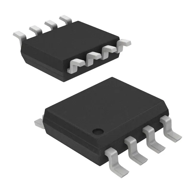
Available in either an 8-pin DIP or SO-8 style respectively,
the ACPL-772L or ACPL-072L optocouplers utilize the
latest CMOS IC technology to achieve outstanding speed
performance of minimum 25MBd data rate and 6ns
maximum pulse width distortion.
•
•
•
•
•
•
•
•
Basic building blocks of this family of products are a
CMOS LED driver IC, a high speed LED and a CMOS
detector IC. A CMOS logic input signal controls the LED
driver IC, which supplies current to the LED. The detector
IC incorporates an integrated photodiode, a high speed
transimpedance amplifier, and a voltage comparator with
an output driver.
Functional Diagram
**VDD1
1
8
V DD2 **
VI
2
7
NC*
NC*
3
6
VO
5
GND 2
IO
LED1
GND 1
4
SHIELD
* Pin 3 is the anode of the internal LED and must be left unconnected
for guaranteed datasheet performance. Pin 7 is not connected
internally.
** A 0.1uF bypass capacitor must be connected between pins 1 and 4,
and 5 and 8.
TRUTH TABLE (POSITIVE LOGIC)
VI, INPUT
LED1
VO, OUTPUT
H
OFF
H
L
ON
L
Dual voltage operation (3.3V and 5V)
Allow level shifting functionality
Support high Speed datarate of 25 MBd
Wide Temperature operation
CMOS output and buffer input
Compatible with CMOS and TTL logic level
Lower power consumption with 3.3V supply
Good AC performance with lower pulse width
distortion
• Lead-free option available
Specifications
•
•
•
•
•
•
•
•
3.3V and 5V CMOS Compatibility
High Speed: DC to 25 MBd
6ns max. Pulse Width Distortion
40 ns max. Prop. Delay
20 ns max. Prop. Delay Skew
10 kV/ms min. Common Mode Rejection
-40 °C to 105 °C Temperature Range
Safety and Regulatory Approvals:
UL Recognised
- 5000Vrms for 1 min. per UL1577 for ACPL-772L
for option 020
- 3750Vrms for 1 min. per UL1577 for ACPL-072L
CSA Component Acceptance Notice #5
IEC/EN/DIN EN 60747-5-2
– VIORM = 630 Vpeak for ACPL-772L Option 060
– VIORM = 560 Vpeak for ACPL-072L Option 060
Applications
•
•
•
•
•
Digital Fieldbus Isolation: DeviceNet, Profibus, SDS
Multiplexed Data Transmission
General Instrument and Data Acquisition
Computer Peripheral interface
Microprocessor System Interface
CAUTION: It is advised that normal static precautions be taken in handling and assembly
of this component to prevent damage and/or degradation, which may be induced by ESD.
�Device Selection Guide
8-Pin DIP
(300 Mil)
Small Outline
SO-8
ACPL-772L
ACPL-072L
Ordering Information
ACPL-072L and ACPL-772L are UL Recognized with 3750 Vrms for 1 minute per UL1577.
Option
Part
number
ACPL-772L
ACPL-072L
RoHS
Compliant
Non RoHS
Compliant
-000E
-
-300E
-
X
X
-500E
-
X
X
-020E
-
-320E
-
-520E
-
-060E
-
-360E
-
X
X
-560E
-
X
X
-000E
No option
X
-500E
-500
-060E
-060
-560E
-560
Package
Surface
Mount
Gull
Wing
Tape
& Reel
UL 5000
Vrms/ 1
Minute
rating
IEC/EN/DIN
EN 607475-2
Quantity
50 per tube
300mil
DIP-8
SO-8
X
X
X
X
X
50 per tube
X
X
X
X
50 per tube
X
50 per tube
X
1000 per reel
X
50 per tube
X
50 per tube
X
1000 per reel
100 per tube
X
X
X
1000 per reel
X
1500 per reel
X
100 per tube
X
1500 per reel
To order, choose a part number from the part number column and combine with the desired option from the option
column to form an order entry.
Example 1:
ACPL-772L-560E to order product of Gull Wing Surface Mount package in Tape and Reel packaging with IEC/EN/DIN
EN 60747-5-2 Safety Approval in RoHS compliant.
Example 2:
ACPL-072L to order product of Small Outline SO-8 package in tube packaging and non RoHS compliant.
Option datasheets are available. Contact your Avago sales representative or authorized distributor for information.
2
�Package Dimensions
ACPL-772L 8-Pin DIP Package
9.65 ± 0.25
(0.380 ± 0.010)
TYPE NUMBER
8
7
7.62 ± 0.25
(0.300 ± 0.010)
6
OPTION 060 CODE*
5
6.35 ± 0.25
(0.250 ± 0.010)
DATE CODE
A XXXXV
YYWW
1
2
3
4
1.78 (0.070) MAX.
1.19 (0.047) MAX.
+ 0.076
- 0.051
+ 0.003)
(0.010 - 0.002)
0.254
5° TYP.
3.56 ± 0.13
(0.140 ± 0.005)
4.70 (0.185) MAX.
0.51 (0.020) MIN.
2.92 (0.115) MIN.
1.080 ± 0.320
(0.043 ± 0.013)
DIMENSIONS IN MILLIMETERS AND (INCHES).
*OPTION 300 AND 500 NOT MARKED.
0.65 (0.025) MAX.
NOTE: FLOATING LEAD PROTRUSION IS 0.25 mm (10 mils) MAX.
2.54 ± 0.25
(0.100 ± 0.010)
ACPL-772L Package with Gull Wing Surface Mount Option 300
LAND PATTERN RECOMMENDATION
9.65 ± 0.25
(0.380 ± 0.010)
8
7
6
1.016 (0.040)
5
6.350 ± 0.25
(0.250 ± 0.010)
1
2
3
10.9 (0.430)
4
1.27 (0.050)
1.19
(0.047)
MAX.
9.65 ± 0.25
(0.380 ± 0.010)
1.780
(0.070)
MAX.
7.62 ± 0.25
(0.300 ± 0.010)
3.56 ± 0.13
(0.140 ± 0.005)
1.080 ± 0.320
(0.043 ± 0.013)
0.635 ± 0.25
(0.025 ± 0.010)
2.54
(0.100)
BSC
DIMENSIONS IN MILLIMETERS (INCHES).
LEAD COPLANARITY = 0.10 mm (0.004 INCHES).
0.635 ± 0.130
(0.025 ± 0.005)
NOTE: FLOATING LEAD PROTRUSION IS 0.25 mm (10 mils) MAX.
3
2.0 (0.080)
+ 0.076
- 0.051
+ 0.003)
(0.010 - 0.002)
0.254
12 ° NOM.
�ACPL-072L Small Outline SO-8 Package
LAND PATTERN RECOMMENDATION
8
7
6
5
XXXV
YWW
3.937 ± 0.127
(0.155 ± 0.005)
5.994 ± 0.203
(0.236 ± 0.008)
TYPE NUMBER
(LAST 3 DIGITS)
7.49 (0.295)
DATE CODE
PIN ONE
1
2
3
4
0.406 ± 0.076
(0.016 ± 0.003)
1.9 (0.075)
1.270 BSC
(0.050)
0.64 (0.025)
* 5.080 ± 0.127
(0.200 ± 0.005)
3.175 ± 0.127
(0.125 ± 0.005)
7°
1.524
(0.060)
45 ° X
0.432
(0.017)
0~7 °
0.228 ± 0.025
(0.009 ± 0.001)
0.203 ± 0.102
(0.008 ± 0.004)
* TOTAL PACKAGE LENGTH (INCLUSIVE OF MOLD FLASH)
5.207 ± 0.254 (0.205 ± 0.010)
DIMENSIONS IN MILLIMETERS (INCHES).
LEAD COPLANARITY = 0.10 mm (0.004 INCHES) MAX.
OPTION NUMBER 500 NOT MARKED.
NOTE: FLOATING LEAD PROTRUSION IS 0.15 mm (6 mils) MAX.
4
0.305 MIN.
(0.012)
�Solder Reflow Temperature Profile
300
PREHEATING RATE 3˚C + 1 ˚C/- 0.5 ˚C/SEC.
REFLOW HEATING RATE 2.5˚C ± 0.5 ˚C/SEC.
TEMPERATURE ( ˚ C)
200
PEAK
TEMP.
245 ˚C
PEAK
TEMP.
240 ˚C
2.5˚ C ± 0.5˚C/SEC.
30
SEC.
160 ˚C
150 ˚C
140 ˚C
PEAK
TEMP.
230˚C
SOLDERING
TIME
200˚C
30
SEC.
3˚C + 1 ˚C/- 0.5 ˚C
100
PREHEATING TIME
150 ˚C, 90 + 30 SEC.
50 SEC.
TIGHT
TYPICAL
LOOSE
ROOM
TEMPERATURE
0
50
0
100
150
TIME (SECONDS)
200
250
Note: Non-halide flux should be used
Recommended Pb-Free IR Profile
tp
Tp
TEMPERATURE
TL
T smax
260 +0/-5 ˚ C
TIME WITHIN 5 ˚ C of ACTUAL
PEAK TEMPERATURE
20-40 SEC.
217 ˚ C
RAMP-UP
3 ˚ C/SEC. MAX.
150 - 200 ˚ C
RAMP-DOWN
6 ˚ C/SEC. MAX.
T smin
ts
PREHEAT
60 to 180 SEC.
tL
60 to 150 SEC.
25
t 25 ˚ C to PEAK
TIME
NO TES:
THE TIME FROM 25 ˚C to PEAK TEMPERATURE = 8 MINUTES MAX.
T smax = 200 ˚ C, T smin = 150 ˚ C
Note: Non-halide flux should be used
Regulatory Information
Both ACPL-072L and ACPL-772L are approved by the following organizations:
IEC/EN/DIN EN 60747-5-2
Approved under:
IEC 60747-5-2:1997 + A1:2002
EN 60747-5-2:2001 + A1:2002
DIN EN 60747-5-2 (VDE 0884 Teil 2):2003-01.
(option 060 only)
5
UL
Approved under UL 1577, component recognition
program up, File E55361.
CSA
Approved under CSA Component Acceptance Notice #5,
File CA 88324.
�Table 1. IEC/EN/DIN EN 60747-5-2 Insulation Characteristics*
ACPL-772L
Option 060
ACPL-072L
Option 060
Installation classification per DIN VDE 0110/1.89, Table 1
for rated mains voltage ≤ 150 Vrms
for rated mains voltage ≤ 300 Vrms
for rated mains voltage ≤ 450 Vrms
I – IV
I – IV
I – III
I – IV
I – III
Climatic Classification
55/105/21
55/105/21
Description
Symbol
Pollution Degree (DIN VDE 0110/1.89)
Units
2
2
Maximum Working Insulation Voltage
VIORM
630
560
Vpeak
Input to Output Test Voltage, Method b**
VIORM x 1.875=VPR, 100% Production Test with tm=1 sec,
Partial discharge < 5 pC
VPR
1181
1050
Vpeak
Input to Output Test Voltage, Method a**
VIORM x 1.5=VPR, Type and Sample Test, tm=60 sec, Partial discharge < 5 pC
VPR
945
840
Vpeak
Highest Allowable Overvoltage (Transient Overvoltage tini = 10 sec)
VIOTM
6000
4000
Vpeak
Safety-limiting values – maximum values allowed in the event of a failure,
also see Figure 2.
Case Temperature
Input Current
Output Power
TS
IS, INPUT
PS, OUTPUT
175
230
600
150
150
600
°C
mA
mW
Insulation Resistance at TS, VIO = 500 V
RIO
>109
>109
W
* Isolation characteristics are guaranteed only within the safety maximum ratings which must be ensured by protective circuits in application.
Surface mount classification is class A in accordance with CECCOO802.
** Refer to the optocoupler section of the Isolation and Control Components Designer’s Catalog, under Product Safety Regulations section IEC/EN/
DIN EN 60747-5-2, for a detailed description of Method a and Method b partial discharge test profiles.
Note: These optocouplers are suitable for “safe electrical isolation” only within the safety limit data. Maintenance of the safety data shall be ensured
by means of protective circuits.
Note: The surface mount classification is Class A in accordance with CECC 00802.
Table 2. Insulation and Safety Related Specifications
Value
Parameter
Symbol
ACPL772L
ACPL-072L
Units
Conditions
Minimum External
Air Gap (Clearance)
L(101)
7.1
4.9
mm
Measured from input terminals to output terminals, shortest distance through air.
Minimum External
Tracking (Creepage)
L(102)
7.4
4.8
mm
Measured from input terminals to output terminals, shortest distance path along body.
0.08
0.08
mm
Through insulation distance conductor to conductor, usually the straight line distance thickness
between the emitter and detector.
>175
>175
V
IIIa
IIIa
Minimum Internal Plastic
Gap (Internal Clearance)
Tracking Resistance
(Comparative Tracking Index)
Isolation Group
CTI
DIN IEC 112/VDE 0303 Part 1
Material Group (DIN VDE 0110, 1/89, Table 1)
All Avago Technologies data sheets report the creepage and clearance inherent to the optocoupler component itself. These dimensions are needed as
a starting point for the equipment designer when determining the circuit insulation requirements. However, once mounted on a printed circuit board,
minimum creepage and clearance requirements must be met as specified for individual equipment standards. For creepage, the shortest distance
path along the surface of a printed circuit board between the solder fillets of the input and output leads must be considered.
There are recommended techniques such as grooves and ribs which may be used on a printed circuit board to achieve desired creepage and clearances.
Creepage and clearance distances will also change depending on factors such as pollution degree and insulation level.
6
�Table 3. Absolute Maximum Ratings
Parameter
Symbol
Min.
Max.
Units
Storage Temperature
TS
–55
+125
°C
Ambient Operating Temperature[1]
TA
–40
+105
°C
Supply Voltages
VDD1, VDD2
0
6.0
Volts
Input Voltage
VI
–0.5
VDD1 +0.5
Volts
Output Voltage
VO
–0.5
VDD2 +0.5
Volts
Average Output Current
IO
10
mA
Lead Solder Temperature
260°C for 10 sec., 1.6 mm below seating plane
Solder Reflow Temperature Profile
Please See Solder Reflow Temperature Profile Section
Table 4. Recommended Operating Conditions
Parameter
Symbol
Min.
Max.
Units
Ambient Operating Temperature
TA
–40
+105
°C
Supply Voltages ( 3.3V operation)
VDD1, VDD2
3.0
3.6
V
Supply Voltages ( 5V operation)
VDD1, VDD2
4.5
5.5
V
Logic High Input Voltage
VIH
2.0
VDD1
V
Logic Low Input Voltage
VIL
0.0
0.8
V
Input Signal Rise and Fall Times
tr, tf
1.0
ms
Table 5. Electrical Specifications
Test conditions that are not specified can be anywhere within the recommended operating range.
The following specifications cover the following power supply combinations: (4.5V≤VDD1≤5.5V, 4.5V≤VDD2≤5.5V),
(3V≤VDD1≤3.6V, 3V≤VDD2≤3.6V), (4.5V≤VDD1≤5.5V, 3V≤VDD2≤3.6V) and (3V≤VDD1≤3.6V, 4.5V≤VDD2≤5.5V).
All typical specifications are at TA=+25°C , VDD1 = VDD2 = +3.3V.
Parameter
Symbol
Logic Low Input Supply Current[2]
Logic High Input Supply Current[2]
Output Supply Current
Min.
Typ.
Max.
Units
Test Conditions
IDD1L
8.8
15
mA
VI = 0 V
IDD1H
1.4
5
mA
VI = VDD1
IDD2L
4.3
10
mA
IDD2H
4.5
10
mA
10
mA
Input Current
II
–10
Logic High Output Voltage
VOH
VDD2 -0.4
VDD2
V
IO = –20 mA, VI = VIH
VDD2 -1.4
VDD2 -0.4
V
IO = –4 mA, VI = VIH
Logic Low Output Voltage
7
VOL
0
0.1
V
IO = 20 mA, VI = VIL
0.35
1.0
V
IO = 4 mA, VI = VIL
�Table 6. Switching Specifications
Test conditions that are not specified can be anywhere within the recommended operating range.
The following specifications cover the following power supply combinations: (4.5V≤VDD1≤5.5V, 4.5V≤VDD2≤5.5V),
(3V≤VDD1≤3.6V, 3V≤VDD2≤3.6V), (4.5V≤VDD1≤5.5V, 3V≤VDD2≤3.6V) and (3V≤VDD1≤3.6V, 4.5V≤VDD2≤5.5V).
All typical specifications are at TA=+25°C, VDD1 = VDD2 = +3.3V.
Parameter
Symbol
Propogation Delay Time
to Logic Low Output [3]
Min.
Typ.
Max.
Units
Test Conditions
tPHL
23.5
40
ns
CL = 15 pF, CMOS Signal Levels
Propogation Delay Time
to Logic High Output [3]
tPLH
25.5
40
ns
CL = 15 pF, CMOS Signal Levels
Pulse Width [4]
tPW
40
Maximum Data Rate [5]
Pulse Width Distortion [6]
|PWD |
2
ns
CL = 15 pF, CMOS Signal Levels
25
MBd
CL = 15 pF, CMOS Signal Levels
6
ns
CL = 15 pF, CMOS Signal Levels
20
ns
CL = 15 pF, CMOS Signal Levels
| tPHL - tPLH |
Propagation Delay Skew [7]
tPSK
Output Rise Time
(10% – 90%)
tR
9
ns
CL = 15 pF, CMOS Signal Levels
Output Fall Time
(90% - 10%)
tF
8
ns
CL = 15 pF, CMOS Signal Levels
Common Mode Transient
Immunity at Logic High Output [8]
| CMH |
10
20
kV/ms
VCM = 1000 V, TA = 25°C,
VI = VDD1, VO > 0.8 VDD1
Common Mode Transient
Immunity at Logic Low Output [8]
| CML |
10
20
kV/ms
VCM = 1000 V, TA = 25°C,
VI = 0 V, VO < 0.8 V
Table 7. Package Characteristics
All typical specifications are at TA = 25°C.
Parameters
Input-Output Momentary
With-stand Voltage [7,8,9]
072L
Symbol
Min.
VISO
3750
772L
3750
772L with
020 option
5000
Typ.
Max.
Units
Test Conditions
V rms
RH ≤ 50%, t = 1 min, TA = 25°C
Input-Output Resistance [9]
R I-O
1012
W
V I-O = 500 V dc
Input-Output Capacitance
C I-O
0.6
pF
f = 1 MHz
CI
3.0
pF
qjci
145
°C/W
Input Capacitance [12]
Input IC Junction-to-Case
Thermal Resistance
772L
Output IC Junction-to-Case
Thermal Resistance
772L
Package Power Dissipation
PPD
072L
072L
160
qjco
140
Thermocouple located at center
underside of package
°C/W
135
150
mW
Notes:
1. Absolute Maximum ambient operating temperature means the device will not be damaged if operated under these conditions. It does not
guarantee functionality.
2. The LED is ON when VI is low and OFF when VI is high.
3. tPHL propagation delay is measured from the 50% level on the falling edge of the VI signal to the 50% level of the falling edge of the VO signal. tPLH
propagation delay is measured from the 50% level on the rising edge of the VI signal to the 50% level of the rising edge of the VO signal.
4. The minimum pulse width is the shortest pulse width at which the specified pulse width distortion is guaranteed.
5. The maximum data rate is the fastest data rate at which the specified pulse width distortion is guaranteed.
6. PWD is defined as |tPHL - tPLH|. %PWD (percent pulse width distortion) is equal to the PWD divided by pulse width.
7. tPSK is equal to the magnitude of the worst case difference in tPHL and/or tPLH that will be seen between units at any given temperature within the
recommended operating conditions.
8
�31
2.40
29
2.20
27
2.00
25
PWD (ns)
Tplh , T phl (ns)
8. CMH is the maximum common mode voltage slew rate that can be sustained while maintaining VO > 0.8 VDD2. CML is the maximum common
mode voltage slew rate that can be sustained while maintaining VO < 0.8 V. The common mode voltage slew rates apply to both rising and falling
common mode voltage edges.
9. Device considered a two-terminal device: pins 1, 2, 3, and 4 shorted together and pins 5, 6, 7, and 8 shorted together.
10. In accordance with UL1577, each ACPL-072L is proof tested by applying an insulation test voltage ≥ 4500 VRMS for 1 second (leakage detection
current limit, II-O ≤ 5 mA). Each ACPL-772L is proof tested by applying an insulation test voltage ≥ 4500 VRMS for 1 second (leakage detection current
limit, II-O ≤ 5 mA).
11. The Input-Output Momentary Withstand Voltage is a dielectric voltage rating that should not be interpreted as an input-output continuous
voltage rating. For the continuous voltage rating refers to your equipment level safety specification or Avago Technologies Application Note 1074
entitled “Optocoupler Input-Output Endurance Voltage.”
12. CI is the capacitance measured at pin 2 (VI).
23
21
1.80
1.60
1.40
19
Tplh
Tphl
17
15
-20
PWD
1.20
1.00
0
20
40
60
80
100
-20
0
20
40
T A ( C)
Figure 1. Typical propagation delays vs temperature
80
100
Figure 2. Typical pulse width distortion vs temperature
12
32
11
30
10
Tplh , T phl (ns)
9
T r , T f (ns)
60
T A ( o C)
o
8
7
6
Rise Time
Fall Time
5
4
-20
28
26
24
20
0
20
40
T A ( o C)
60
80
Tplh
Tphl
22
100
15
25
35
C L (pF)
45
55
Figure 4. Typical propagation delays vs load capacitance
Figure 3. Typical rise and fall time vs temperature
6
PWD
5
Surface Mount SO-8 Product
3
2
1
0
15
25
35
C L (pF)
45
Figure 5. Typical pulse width distortion vs load capacitance
9
55
1000
Is (mA)
800
Output Power - Ps, Input Current - Is
Output Power - Ps, Input Current - Is
PWD (ns)
4
Standard 8-pin DIP Product
1,000
Ps (mW)
600
400
200
0
0
25
50
75
100
125
TA - Case Temperature - C
150
175
Is (mA)
Ps (mW)
800
600
400
200
0
0
25
50
75 100 125 150
TA - Case Temperature - °C
175
Figure 6. Thermal derating curve, dependence of safety limiting value with
case temperature per IEC/EN/DIN EN 60747-5-2
�Application Information
Propagation Delay, Pulse-Width Distortion and Propagation Delay Skew
Bypassing and PC Board Layout
The ACPL-x72L optocouplers are extremely easy to use.
No external interface circuitry is required because ACPLx72L uses high speed CMOS IC technology allowing
CMOS logic to be connected directly to the inputs and
outputs.
As shown in Figure 7, the only external components
required for proper operation are two bypass capacitors.
Capacitor values should be between 0.01mF and 0.1mF.
For each capacitor, the total lead length between both
ends of the capacitor and power supply pins should not
exceed 20mm. Figure 8 illustrates the recommended
printed circuit board layout for ACPL-x72L.
V DD1
VI
C1
50%
VI
t PLH
OUTPUT
VO
10%
90%
7 NC
90%
10%
4
6
5
VO
GND 2
C1, C2 = 0.01 µF TO 0.1 µF
Figure 7. Recommended Circuit Diagram
0V
V OH
2.5 V CMOS
V OL
Pulse-width distortion (PWD) is the difference between
tPHL and tPLH and often determines the maximum data
rate capability of a transmission system. PWD can be
expressed in percent by dividing the PWD (in ns) by the
minimum pulse width (in ns) being transmitted. Typically,
PWD on the order of 20-30% of the minimum pulse
width is tolerable. The PWD specification for ACPL-x72L
is 6ns (15%) maximum across recommended operating
conditions.
V DD1
VDD2
VI
72L
YYL
C1
5 V CMOS
Figure 9. Signal plot shows how propagation delay is defined
72L
YYL
NC 3
C2
VO
GND 1
GND 2
C1, C2 = 0.01 µF TO 0.1 µF
Figure 8. Recommended Printed Circuit Board Layout
10
t PHL
C2
2
GND1
INPUT
V DD2
8
1
Propagation Delay is a figure of merit which describes
how quickly a logic signal propagates through a system.
The propagation delay from a low to high (tPLH) is the
amount of time required for an input signal to propagate
to the output, causing the output to change from low to
high. Similarly, the propagation delay from high to low
(tPHL) is the amount of time required for the input signal
to propagate to the output, causing the output to change
from high to low. Please see Figure 9.
�Propagation delay skew, tPSK, is an important parameter
to consider in parallel data applications where
synchronization of signals on parallel data lines is a
concern. If the parallel data is sent through a group
of optocouplers, differences in propagation delays
will cause the data to arrive at the outputs of the
optocouplers at different times. If this difference in
propagation delay is large enough it will determine the
maximum rate at which parallel data can be sent through
the optocouplers.
As mentioned earlier, tPSK can determine the maximum
parallel data transmission rate. Figure 11 is the timing
diagram of a typical parallel data application with
both the clock and data lines being sent through the
optocouplers. The figure shows data and clock signals at
the inputs and outputs of the optocouplers. In this case
the data is assumes to be clocked off of the rising edge of
the clock.
Propagation delay skew is defined as the difference
between the minimum and maximum propagation
delays, either tPLH or tPHL for any given group of
optocouoplers which are operating under the same
conditions (i.e., the same drive current, supply voltage,
output load, and operating temperature). As illustrated
in Figure 10, if the inputs of a group of optocouplers are
switched either ON or OFF at the same time, tPSK is the
difference between the shortest propagation delay,
either tPLH or tPHL and the longest propagation delay,
either tPLH and tPHL.
INPUTS
DATA
CLOCK
DATA
OUTPUTS
t PSK
CLOCK
t PSK
VI
VO
50%
Figure 11. Parallel data transmission example.
2.5 V,
CMOS
t PSK
VI
VO
50%
2.5 V,
CMOS
Figure 10. Propagation delay skew waveform
Propagation delay skew represents the uncertainty
of where an edge might be after being sent through
an optocoupler. Figure 11 shows that there will be
uncertainty in both the data and clock lines. It is
important that these two areas of uncertainty not
overlap, otherwise the clock signal might arrive before
all the data outputs have settled, or some of the data
outputs may start to change before the clock signal
has arrived. From these considerations, the absolute
minimum pulse width that can be sent through
optocouplers in a parallel application is twice tPSK. A
cautious design should use a slightly longer pulse width
to ensure that any additional uncertainty in the rest of
the circuit does not cause a problem.
The ACPL-x72L optocoupler offers the advantage of
guaranteed specifications for propagation delays, pulsewidth distortion, and propagation delay skew over the
recommended temperature and power supply ranges.
For product information and a complete list of distributors, please go to our web site:
www.avagotech.com
Avago, Avago Technologies, and the A logo are trademarks of Avago Technologies in the United States and other countries.
Data subject to change. Copyright © 2005-2010 Avago Technologies. All rights reserved. Obsoletes AV01-0462EN
AV02-0324EN - January 19, 2010
�


 工商网监
湘ICP备2023018690号
工商网监
湘ICP备2023018690号
