Data Sheet
ACPL-217
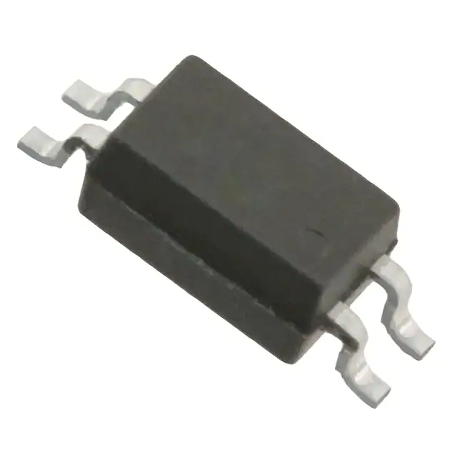
DC-Input, Half-Pitch Phototransistor Optocoupler
Description
Features
The Broadcom® ACPL-217 is a DC-input, single-channel,
half-pitch phototransistor optocoupler that contains a
light-emitting diode optically coupled to a phototransistor. It
is packaged in a 4-pin SO package.
The input-output isolation voltage is rated at 3750VRMS.
Response time, tr, is 2 μs typically, while minimum CTR is
50% at input current of 5 mA.
ACPL-217 Pin Layout
4
3
Current transfer ratio (CTR): 50% (minimum) at
IF = 5 mA, VCC = 5V
High input-output isolation voltage (VISO): 3750VRMS
Non-saturated response time (tr): 2 μs (typical) at
VCC = 10V, IC = 2 mA, RL= 100Ω
SO package
CMR: 10 kV/μs (typical)
Safety and regulatory approvals
– cUL
– IEC/EN/DIN EN 60747-5-2
Available options
– CTR Ranks 0, A, B, C, and D
Applications
1
2
Pin
Description
1
Anode
2
Cathode
3
Emitter
4
Collector
I/O Interface for programmable controllers, computers
Sequence controllers
System appliances, measuring instruments
Signal transmission between circuits of different
potentials and impedances
CAUTION! It is advised that normal static precautions be taken in handling and assembly of this component to prevent
damage and/or degradation which may be induced by ESD.
The components featured in this data sheet are not to be used in military or aerospace applications or
environments.
Broadcom
AV02-0470EN-DS104
October 7, 2022
�ACPL-217 Data Sheet
DC-Input, Half-Pitch Phototransistor Optocoupler
Ordering Information
Rank C
200% <
CTR <
400%
IF = 5 mA,
VCE = 5V
Rank D
300% <
CTR <
600%
IF = 5 mA
VCE = 5V
Tape & Reel
ACPL
-217
-500E
-50AE
-50BE
-50CE
-50DE
SO-4
X
X
-560E
-56AE
-56BE
-56CE
-56DE
SO-4
X
X
0°
-700E
-70AE
-70BE
-70CE
-70DE
SO-4
X
X
180°
-760E
-76AE
-76BE
-76CE
-76DE
SO-4
X
X
180°
IC Orientation
Rank B
130% <
CTR <
260%
IF = 5mA,
VCE = 5V
Rank 0
50% <
CTR <
600%
IF = 5 mA,
Part
Number VCE = 5V
Package
Rank A
80% <
CTR <
160%
IF = 5 mA,
VCE = 5V
Surface Mount
RoHS Compliant Option
IEC/EN/DIN EN
60747-5-2
ACPL-217-xxxx is UL recognized with 3750VRMS for 1 minute per UL1577 and Canadian Component Acceptance Notice #5.
0°
Quantity
3000 pieces per reel
X
3000 pieces per reel
3000 pieces per reel
X
3000 pieces per reel
To order, choose a part number from the part number column and combine with the desired option from the option column
to form an order entry.
Example: Specify ACPL-217-560E to order the following product: SO-4 Surface Mount package in Tape & Reel
packaging, with IEC/EN/DIN EN 60767-5-2 Safety Approval, 50% < CTR < 600%, and RoHS compliant.
Example: Specify ACPL-217-50BE to order the following product: SO-4 Surface Mount package in Tape & Reel
packaging, with 130% < CTR < 260%, and RoHS compliant.
Option data sheets are available. Contact your Broadcom sales representative or authorized distributor for information.
Package Outline Drawings
Broadcom
AV02-0470EN-DS104
2
�ACPL-217 Data Sheet
DC-Input, Half-Pitch Phototransistor Optocoupler
Solder Reflow Temperature Profile
Recommended reflow condition as per JEDEC Standard, J-STD-020 (latest revision). Non-Halide Flux should be used.
Absolute Maximum Ratings
Parameter
Symbol
ACPL-217
Unit
Note
Storage Temperature
TS
–55 to 125
°C
—
Operating Temperature
TA
–55 to 110
°C
—
Average Forward Current
IF(AVG)
50
mA
—
Pulse Forward Current
IFSM
1
A
—
Reverse Voltage
VR
6
V
—
LED Power Dissipation
PI
65
mW
—
Collector Current
IC
50
mA
—
Collector-Emitter Voltage
VCEO
80
V
—
Emitter-Collector Voltage
VECO
7
V
—
Isolation Voltage (AC for 1 min, R.H. 40 to 60%)
VISO
3750
VRMS
1 min
Collector Power Dissipation
PC
150
mW
—
Total Power Dissipation
PTOT
200
mW
—
Lead Solder Temperature
Broadcom
260°C for 10 seconds
AV02-0470EN-DS104
3
�ACPL-217 Data Sheet
DC-Input, Half-Pitch Phototransistor Optocoupler
Electrical Specifications (DC)
Over recommended ambient temperature at 25°C unless otherwise specified.
Parameter
Symbol
Min.
Typ.
Max.
Unit
Test Conditions
Note
Forward Voltage
VF
—
1.2
1.4
V
IF = 20 mA
Figure 6
Reverse Current
IR
—
—
10
μA
VR = 5V
—
Terminal Capacitance
Ct
—
30
—
pF
V = 0, f = 1 MHz
—
Collector Dark Current
ICEO
—
—
100
nA
VCE = 48V, IF = 0 mA
Figure 12
Collector-Emitter Breakdown Voltage
BVCEO
80
—
—
V
IC = 0.5 mA, IF = 0 mA
—
Emitter-Collector Breakdown Voltage
BVECO
7
—
—
V
IE = 100 μA, IF = 0 mA
—
Current Transfer Ratio
CTR
50
—
600
%
IF = 5 mA, VCE = 5V
CTR = (IC/IF) *
100%
Saturated CTR
CTR(sat)
—
100
—
%
IF = 1 mA, VCE = 0.4V
—
Collector-Emitter Saturation Voltage VCE(sat)
—
—
0.4
V
IF = 8 mA, IC = 2.4 mA
Figure 14
—
Ω
DC500V, R.H. 40~60%
—
Isolation Resistance
RISO
Floating Capacitance
CF
—
0.6
1
pF
V = 0, f = 1 MHz
—
Cut-off Frequency (–3 dB)
FC
—
80
—
kHz
VCC = 5V, IC = 2 mA, RL = 100Ω
Figure 2,
Figure 19
Response Time (Rise)
tr
—
2
—
μs
Figure 1
Response Time (Fall)
tf
—
3
—
μs
VCC = 10V, IC = 2 mA,
RL = 100Ω
Turn-on Time
ton
—
3
—
μs
Turn-off Time
toff
—
3
—
μs
Turn-ON Time
tON
—
2
—
μs
Storage Time
TS
—
25
—
μs
VCC = 5V, IF = 16 mA,
RL = 1.9 kΩ
Figure 1,
Figure 17
Turn-OFF Time
tOFF
—
40
—
μs
Common Mode Rejection Voltage
CMR
—
10
—
kV/μs
TA = 25°C, RL = 470Ω,
VCM = 1.5 kV(peak), IF = 0 mA,
VCC = 9V, Vnp = 100 mV
Figure 20
5 x 10¹⁰ 1 x 10¹¹
Figure 1: Switching Time Test Circuit
IF
RL
VCC
VCE
IF
VCE
tr
tf
ts
90%
10%
ton
toff
Figure 2: Frequency Response Test Circuit
RL
VCC
Output
RD
Broadcom
AV02-0470EN-DS104
4
�ACPL-217 Data Sheet
DC-Input, Half-Pitch Phototransistor Optocoupler
Figure 3: Forward Current vs. Ambient Temperature
Figure 4: Collector Power Dissipation vs. Ambient
Temperature
160
60
40
ACPL-217
30
20
10
-5
15
35
55
Ambient Temperature, Ta(º C)
75
95
ACPL-217
100
80
60
40
0
-25
115
Figure 5: Pulse Forward Current vs. Duty Cycle Ratio
0
25
50
75
Ambient Temperature, Ta(º C)
100
125
Figure 6: Forward Current vs. Forward Voltage
100
10000
Pulse width ≤100 Ps
Ta = 25 º C
Forward Current, I F (mA)
Peak Forward Current, I FP (mA)
120
20
0
-25
1000
100
10
0.0001
0.0010
0.0100
Duty Ratio
0.1000
50 º C
-30º C
0ºC
25 º C
75 º C
Ta = 110 ºC
10
1
0.4
1.0000
Figure 7: Forward Voltage Temperature Coefficient vs.
Forward Current
0.6
0.8
1.0
1.2
1.4
Forward Voltage, V F (V)
1.6
1.8
2.0
Figure 8: Pulse Forward Current vs. Pulse Forward Voltage
1000
-3.2
-2.8
Pulse Forward Current, I FP (mA)
Forward Voltage Temperature Coefficient
'V F /'Ta (mV/ º C)
140
Collector Power Dissipation, Pc(mW)
Forward Current, I F (mA)
50
-2.4
-2.0
-1.6
-1.2
-0.8
-0.4
Broadcom
0.1
1
10
Forward current, I F (mA)
100
100
10
1
0.5
Pulse Width ≤10 Ps
Repetitive
Frequency=100Hz
Ta=25ºC
1
1.5
2
Pulse Forward Voltage, V FP (V)
2.5
3
AV02-0470EN-DS104
5
�ACPL-217 Data Sheet
DC-Input, Half-Pitch Phototransistor Optocoupler
Figure 9: Collector Current vs. Collector-Emitter Voltage
Figure 10: Collector Current vs. Small Collector-Emitter
Voltage
50
50
Ta = 25º C
45
50mA
50mA
40
40
Collector Currrent, Ic( mA)
Collector Current, Ic(mA)
30mA
20mA
30
P C (max)=150mW
20
10mA
30mA
30
25
20mA
20
10mA
15
10
10
0
0
5
Collector-Emitter Voltage, Vce(V)
10
Figure 11: Collector Current vs. Forward Current
5mA
5
I F =5mA
0
35
IF = 2mA
0
0.5
Collector-Emitter Voltage, V CE (V)
1
Figure 12: Collector Dark Current vs. Ambient Temperature
0.1
10V
1.E-06
Collector Dark Current, I CEO (A)
Collector Current, I C (A)
5V
V CE = 0.4V
0.01
0.001
0.0001
0.0001
-25
0.1
-5
15
35
55
Ambient Temperature, Ta(°C)
75
95
0.18
Collector-Emitter Saturation Voltage, V CE (sat) (V)
Current Transfer Ratio, CTR (%)
5V
10V
Figure 14: Collector-Emitter Saturation Voltage vs. Ambient
Temperature
1000
10V
5V
VCE = 0.4V
100
Broadcom
24V
1.E-10
0.001
0.01
Forward Current, I F (A)
Figure 13: Current Transfer Ratio vs. Forward Current
10
0.0001
V CE = 48V
1.E-08
0.001
0.01
Forward Current, I F (A)
0.1
0.16
0.14
0.12
I F = 8mA,
I C = 2.4mA
0.10
IF = 20mA,
IC = 1mA
0.08
IF = 1mA,
IC = 0.2mA
0.06
0.04
0.02
0.00
-30
5
40
Ambient Temperature, Ta(º C)
75
110
AV02-0470EN-DS104
6
�ACPL-217 Data Sheet
DC-Input, Half-Pitch Phototransistor Optocoupler
Figure 15: Collector Current vs. Ambient Temperature
100
Figure 16: Switching Time vs. Load Resistance
1000
IF=16mA
VCC=5V
Ta=25°C
TOFF
25mA
6ZLWFKLQJ�7LPH��W��V�
Collector Current, I C (mA)
100
10mA
10
5mA
1mA
1
TS
10
1
I F = 0.5mA
0.1
-25
TON
0
0
25
50
Ambient Temperature, Ta ( o C)
75
100
Figure 17: Switching Time vs. Ambient Temperature
1
10
/RDG�5HVLVWDQFH��5/��Nȍ�
50
100
Figure 18: Collector-Emitter Saturation Voltage vs. Forward
Current
5
10
t ON
1
I F = 16mA
V CC = 5V
RL = 1.9k:
0.1
-20
0
20
40
60
Ambient Temperature, Ta ( ºC)
80
100
Figure 19: Frequency Response
4
3
5mA
tS
Ta = 25ºC
2
7mA
I C = 10mA
Collector-Emitter Saturation Voltage, V CE(sat) (V)
t OFF
0.5mA
1mA
3mA
100
Switching Time, t (Ps)
5
1
0
0
5
10
Forward Current, I F (mA)
15
20
Figure 20: CMR Test Circuit
0
dV/dt
RL = 100:
Vcc
-2
RL
V np
470 :
1k:
Vo, (dB)
Vo
V CM
9V
Vo
-4
V CM
(High Voltage Pulse)
V cp
Vcp » (dV/dt)xCfxRL
Vcp: Voltage that is generated by the displacement
current in floating capacitance between primary and
secondary sides.
-6
V cc = 5V
I C = 2mA
Ta = 25ºC
-8
1
Broadcom
10
Frequency, f (kHz)
100
AV02-0470EN-DS104
7
�Copyright © 2005–2022 Broadcom. All Rights Reserved. The term “Broadcom” refers to Broadcom Inc. and/or its
subsidiaries. For more information, go to www.broadcom.com. All trademarks, trade names, service marks, and logos
referenced herein belong to their respective companies.
Broadcom reserves the right to make changes without further notice to any products or data herein to improve reliability,
function, or design. Information furnished by Broadcom is believed to be accurate and reliable. However, Broadcom does
not assume any liability arising out of the application or use of this information, nor the application or use of any product or
circuit described herein, neither does it convey any license under its patent rights nor the rights of others.
�