ACPL-C87B, ACPL-C87A, ACPL-C870
Precision Optically Isolated Voltage Sensor
Data Sheet
Lead (Pb) Free
RoHS 6 fully
compliant
RoHS 6 fully compliant options available;
-xxxE denotes a lead-free product
Description
Features
The ACPL-C87B/C87A/C870 voltage sensors are optical
isolation amplifiers designed specifically for voltage
sensing. Its 2 V input range and high 1 GΩ input impedance, makes it well suited for isolated voltage sensing
requirements in electronic power converters applications
including motor drives and renewable energy systems.
In a typical voltage sensing implementation, a resistive
voltage divider is used to scale the DC-link voltage to suit
the input range of the voltage sensor. A differential output
voltage that is proportional to the input voltage is created
on the other side of the optical isolation barrier.
Advanced Sigma-Delta (Σ-Δ) Modulation Technology
For general applications, the ACPL-C87A (±1% gain
tolerance) and the ACPL-C870 (±3% gain tolerance)
are recommended. For high precision requirements,
the ACPL-C87B (±0.5% gain tolerance) can be used. The
ACPL-C87B/C87A/C870 family operates from a single 5 V
supply and provides excellent linearity. An active-high
shutdown pin is available which reduces the IDD1 current
to only 15 μA, making them suitable for battery-powered
and other power-sensitive applications.
3 V to 5.5 V Wide Supply Range for Output Side
The high common-mode transient immunity (15 kV/s)
of the ACPL-C87B/C87A/C870 provides the precision and
stability needed to accurately monitor DC-link voltage in
high noise environments. Combined with superior optical
coupling technology, the ACPL-C87B/C87A/C870 implements sigma-delta (Σ-Δ) modulation, chopper stabilized
amplifiers, and differential outputs to provide unequaled
isolation-mode noise rejection, low offset, high gain
accuracy and stability. This performance is delivered in a
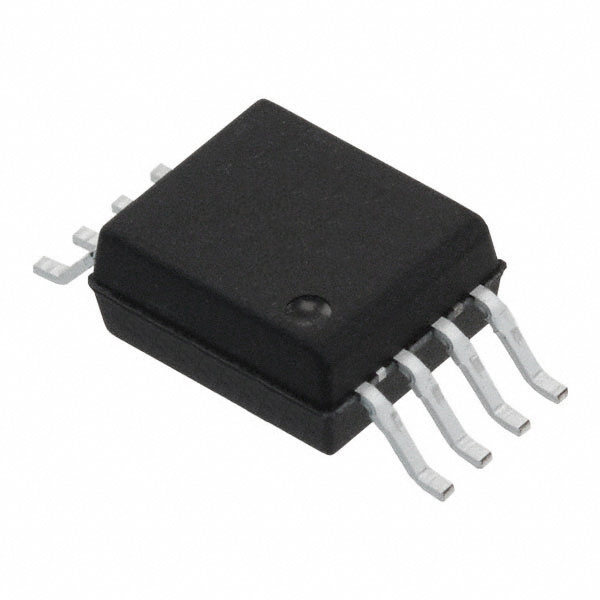
compact, auto-insertable Stretched SO-8 (SSO-8) package
that meets worldwide regulatory safety standards.
Unity Gain 1 V/V, ±0.5% High Gain Accuracy (ACPL-C87B)
1 GΩ Input Impedence
0 to 2 V Nominal Input Range
-35 ppm/°C Low Gain Drift
21 μV /°C Offset Voltage Drift
0.1% Non-Linearity Max
Active-High Shutdown Pin
100 kHz Wide Bandwidth
-40° C to +105° C Operating Temperature Range
15 kV/s Common-Mode Transient Immunity
Compact, Auto-Insertable Stretched SO-8 Package
Safety and Regulatory Approvals:
– IEC/EN/DIN EN 60747-5-5: 1414 Vpeak working
insulation voltage
– UL 1577: 5000 Vrms/1 min double protection rating
– CSA: Component Acceptance Notice #5
Applications
Isolated Voltage Sensing in AC and Servo Motor Drives
Isolated DC-Bus Voltage Sensing in Solar Inverters,
Wind Turbine Inverters
Isolated Sensor Interfaces
Signal Isolation in Data Acquisition Systems
General Purpose Voltage Isolation
CAUTION: It is advised that normal static precautions be taken in handling and assembly
of this component to prevent damage and/or degradation which may be induced by ESD.
�Functional Diagram
VDD1 1
8 VDD2
VIN 2
7 VOUT+
SHDN 3
6 VOUT–
GND1 4
5 GND2
SHIELD
Table 1. Pin Description
Figure 1.
NOTE: A 0.1 μF bypass capacitor must be connected between pins 1 and
4 and between pins 5 and 8.
Pin No.
Symbol
Description
1
VDD1
Supply voltage for input side
(4.5 V to 5.5 V), relative to GND1
2
VIN
Voltage input
3
SHDN
Shutdown pin (Active High)
4
GND1
Input side ground
5
GND2
Output side ground
6
VOUT-
Negative output
7
VOUT+
Positive output
8
VDD2
Supply voltage for output side
(3 V to 5.5 V), referenced to GND2
Ordering Information
ACPL-C87B/C87A/C870 is UL recognized with 5000 Vrms/1 minute rating per UL 1577.
Table 2.
Option
Part number
(RoHS Compliant)
Package
Surface Mount
ACPL-C87B
ACPL-C87A
ACPL-C870
-000E
Stetched
SO-8
X
-500E
X
Tape &
Reel
X
IEC/EN/DIN EN
60747-5-5
Quantity
X
80 per tube
X
1000 per reel
To order, choose a part number from the part number column and combine with the desired option from the option
column to form an order entry.
Example:
ACPL-C87A-500E to order product of Surface Mount package in Tape and Reel packaging with IEC/EN/DIN EN 60747-5-5
Safety Approval and RoHS compliance.
Contact your Avago sales representative or authorized distributor for information.
2
�Package Outline Drawing
Stretched SO-8 Package (SSO-8)
RECOMMENDED LAND PATTERN
5.850 ± 0.254
(0.230 ± 0.010)
PART NUMBER
8
RoHS-COMPLIANCE
INDICATOR
7
6
5
C87B
YWW
EEE
1
2
3
DATE CODE
12.650
(0.498)
6.807 ± 0.127
(0.268 ± 0.005)
1.905
(0.075)
4
LOT ID
7°
3.180 ± 0.127
(0.125 ± 0.005)
0.381 ± 0.127
(0.015 ± 0.005)
0.64
(0.025)
1.590 ± 0.127
(0.063 ± 0.005)
45°
0.450
(0.018)
0.750 ± 0.250
(0.0295 ± 0.010)
11.50 ± 0.250
(0.453 ± 0.010)
0.200 ± 0.100
(0.008 ± 0.004)
1.270
(0.050) BSG
0.254 ± 0.100
(0.010 ± 0.004)
Dimensions in millimeters and (inches).
Figure 2. SSO-8 Package
Note:
Lead coplanarity = 0.1 mm (0.004 inches).
Floating lead protrusion = 0.25mm (10mils) max.
Recommended Pb-Free IR Profile
Recommended reflow condition as per JEDEC Standard, J-STD-020 (latest revision). Non-Halide Flux should be used.
Regulatory Information
The ACPL-C87B/C87A/C870 is approved by the following organizations:
IEC/EN/DIN EN 60747-5-5
Approval with Maximum Working Insulation Voltage VIORM = 1414 Vpeak.
UL
Approval under UL 1577, component recognition program up to VISO = 5000 Vrms/1 min. File 55361.
CSA
Approval under CSA Component Acceptance Notice #5, File CA 88324
3
�Table 3. Insulation and Safety Related Specifications
Parameter
Symbol
Value
Unit
Conditions
Minimum External Air Gap
(External Clearance)
L(101)
8.0
mm
Measured from input terminals to output terminals,
shortest distance through air
Minimum External
Tracking (External Creepage)
L(102)
8.0
mm
Measured from input terminals to output terminals,
shortest distance path along body
0.5
mm
Through insulation distance, conductor to conductor,
usually the direct distance between the photoemitter
and photodetector inside the optocoupler cavity
> 175
V
DIN IEC 112/VDE 0303 Part 1
Minimum Internal Plastic Gap
(Internal Clearance)
Tracking Resistance
(Comparative Tracking Index)
CTI
Isolation Group
IIIa
Material Group (DIN VDE 0110, 1/89, Table 1)
Table 4. IEC/EN/DIN EN 60747-5-5 Insulation Characteristics [1]
Description
Symbol
Value
Installation classification per DIN VDE 0110/1.89, Table 1
for rated mains voltage ≤ 150 Vrms
for rated mains voltage ≤ 300 Vrms
for rated mains voltage ≤ 450 V rms
for rated mains voltage ≤ 600 Vrms
for rated mains voltage ≤ 1000 Vrms
I-IV
I-IV
I-IV
I-IV
I-III
Climatic Classification
55/105/21
Pollution Degree (DIN VDE 0110/1.89)
Units
2
Maximum Working Insulation Voltage (Pending Qualification)
VIORM
1414
Vpeak
Input to Output Test Voltage, Method b
VIORM x 1.875 = VPR, 100% Production Test with tm = 1 sec, Partial Discharge < 5 pC
VPR
2652
Vpeak
Input to Output Test Voltage, Method a
VIORM x 1.6 = VPR, Type and Sample Test, tm = 10 sec, Partial Discharge < 5 pC
VPR
2262
Vpeak
Highest Allowable Overvoltage (Transient Overvoltage, tini = 60 sec)
VIOTM
8000
Vpeak
Safety-limiting values (Maximum values allowed in the event of a failure)
Case Temperature
Input Current [2]
Output Power [2]
TS
IS,INPUT
PS,OUTPUT
175
230
600
°C
mA
mW
Insulation Resistance at TS, VIO = 500 V
RS
≥ 109
Notes:
1. Insulation characteristics are guaranteed only within the safety maximum ratings, which must be ensured by protective circuits within the
application.
4
�Table 5. Absolute Maximum Rating
Parameter
Symbol
Min.
Max.
Units
Storage Temperature
TS
-55
+125
°C
Ambient Operating Temperature
TA
-40
+105
°C
Supply Voltage
VDD1, VDD2
-0.5
6.0
V
Steady-State Input Voltage [1, 3]
VIN
-2
VDD1 + 0.5
V
Two-Second Transient Input Voltage [2]
VIN
-6
VDD1 + 0.5
V
Logic Input
VSD
-0.5
VDD1 + 0.5
V
Output Voltages
VOUT+, VOUT−
-0.5
VDD2 + 0.5
V
Lead Solder Temperature
260° C for 10 sec., 1.6 mm below seating plane
Notes:
1. DC voltage of up to -2 V on the inputs does not cause latch-up or damage to the device.
2. Transient voltage of 2 seconds up to -6 V on the inputs does not cause latch-up or damage to the device.
3. Absolute maximum DC current on the inputs = 100 mA, no latch-up or device damage occurs.
Table 6. Recommended Operating Conditions
Parameter
Symbol
Min.
Max.
Units
Ambient Operating Temperature
TA
-40
+105
°C
VDD1 Supply Voltage
VDD1
4.5
5.5
V
VDD2 Supply Voltage
VDD2
3.0
5.5
V
Input Voltage Range[1]
VIN
0
2.0
V
Shutdown Enable Voltage
VSD
VDD1 – 0.5
VDD1
V
Notes:
1. 2 V is the nominal input range. Full scale input range (FSR) is 2.46 V.
5
�Table 7. Electrical Specifications
Unless otherwise noted, TA = -40° C to +105° C, VDD1 = 4.5 V to 5.5 V, VDD2 = 3.3 V to 5.5 V, VIN = 0 – 2 V, and VSD = 0 V.
Parameter
Symbol
Min.
Typ.[1]
Max.
-9.9
-0.3
9.9
Unit
Test Conditions/Notes
Fig.
DC CHARACTERISTICS
Input Offset Voltage
VOS
Magnitude of Input Offset
Change vs. Temperature
|dVOS/dTA|
Gain (ACPL-C87B, ±0.5%)
G0
21
mV
TA = 25° C
3, 4
V/°C
TA = –40° C to +105° C
; Direct short across inputs.
5
0.995
1
1.005
V/V
TA = 25° C; VDD2 = 5 V;
Note 2.
6, 7
0.994
0.999
1.004
V/V
TA = 25° C; VDD2 = 3.3 V;
Note 2.
6, 7
Gain (ACPL-C87A, ±1%)
G1
0.99
1
1.01
V/V
TA = 25° C; Note 2.
6, 7
Gain (ACPL-C870, ±3%)
G3
0.97
1
1.03
V/V
TA = 25° C; Note 2.
6, 7
Magnitude of Gain Change
vs. Temperature
dG/dTA
-35
ppm/°C
TA = -40° C to +105° C
8
Nonlinearity
NL
0.05
%
VIN = 0 to 2 V, TA = 25° C
9, 10
Magnitude of NL Change
vs. Temperature
|dNL/dTA|
0.0002
%/°C
TA = -40° C to +105° C
11
Recommended Input Range
VINR
2
V
Referenced to GND1
Full-Scale Differential Voltage
Input Range
FSR
2.46
V
Referenced to GND1
Shutdown Logic Low
Input Voltage
VIL
0.8
Shutdown Logic High
Input Voltage
VIH
VDD – 0.5 5
Input Bias Current
IIN
-0.1
Magnitude of IIN Change
vs. Temperature
0.1
INPUTS AND OUTPUTS
TA = 25° C
TA = 25° C
-0.0015
A
dIIN/dTA
1
nA/°C
Equivalent Input Impedance
RIN
1000
M
Output Common-Mode
Voltage
VOCM
1.23
V
VOUT+ or VOUT–
Output Voltage Range
VOUTR
Vocm ±
1.23
V
VSD = 0 V. Note 4.
Output Short-Circuit Current
|IOSC|
30
mA
VOUT+ or VOUT–,
shorted to GND2 or VDD2
Output Resistance
ROUT
36
VOUT+ or VOUT–
6
VIN = 0 V
13
�Table 7. Electrical Specifications (continued)
Unless otherwise noted, TA = -40° C to +105° C, VDD1 = 4.5 V to 5.5 V, VDD2 = 3.3 V to 5.5 V, VIN = 0 – 2 V, and VSD = 0 V.
Parameter
Symbol
Typ.[1]
Min.
Max.
Unit
Test Conditions/Notes
Fig.
mVrms
Vin = 0 V;
Output low-pass filtered
to 180 KHz. Note 3.
12
AC CHARACTERISTICS
Vout Noise
Nout
0.013
Small-Signal Bandwidth (-3 dB)
f–3 dB
kHz
Guaranteed by design
Input to Output
Propagation Delay
50%-10%
tPD10
70
100
2.2
3.0
s
Step input.
18
50%-50%
tPD50
3.7
5.5
s
Step input.
18
18
tPD90
5.3
6.5
s
Step input.
Output Rise/Fall Time (10%-90%)
tR/F
2.7
4.0
s
Step input (tPD90 - tPD10)
Shutdown Delay
tSD
25
40
s
Vin = 2 V
Enable Delay
tON
150
200
s
Common Mode Transient Immunity
CMTI
Power Supply Rejection
50%-90%
15
kV/s
VCM = 1 kV, TA = 25° C
PSR
-78
dB
1 Vpp 1 kHz sine wave
ripple on VDD1,
differential output
IDD1
10.5
mA
VSD = 0 V
A
VSD = 5 V
IDD2
6.5
12
mA
5 V supply
6.1
11
mA
3.3 V supply
10
17
POWER SUPPLIES
Input Side Supply Current
15
15
Notes:
1. All Typical values are under Typical Operating Conditions at TA = 25° C, VDD1 = 5 V, VDD2 = 5 V.
2. Gain is defined as the slope of the best-fit line of differential output voltage (VOUT+ – VOUT-) versus input voltage over the nominal range, with offset
error adjusted.
3. Noise is measured at the output of the differential to single ended post amplifier.
4. When is VSD = 5 V or when shutdown is enabled, Vout+ is close to 0V and Vout- is at close to 2.46 V. This is similar to when VDD1 is not supplied.
Table 8. Package Characteristics
Parameter
Symbol
Min
Input-Output Momentary
Withstand Voltage
VISO
5000
Resistance (Input-Output)
RI-O
Capacitance (Input-Output)
CI-O
Typ
Max
Units
Test Conditions
Note
Vrms
RH < 50%, t = 1 min.,
TA = 25° C
1, 2
> 1012
VI-O = 500 VDC
3
0.5
pF
f = 1 MHz
3
Notes:
1. In accordance with UL 1577, each optocoupler is proof tested by applying an insulation test voltage ≥ 6000 Vrms for 1 second (leakage detection
current limit, II-O ≤ 5 μA). This test is performed before the 100% production test for partial discharge (method b) shown in IEC/EN/DIN EN 607475-5 Insulation Characteristic Table.
2. The Input-Output Momentary Withstand Voltage is a dielectric voltage rating that should not be interpreted as an input-output continuous
voltage rating. For the continuous voltage rating, refer to the IEC/EN/DIN EN 60747-5-5 insulation characteristics table and your equipment level
safety specification.
3. This is a two-terminal measurement: pins 1–4 are shorted together and pins 5–8 are shorted together.
7
�Typical Performance Plots
5
4
3
2
1
0
-1
-2
-3
-4
-5
2
1.5
1
Offset (mV)
Offset (mV)
All ±3(sigma symbol) plots are based on characterization test result at the point of product release. For guaranteed
specification, refer to the respective Electrical Specifications section.
-0.5
-1.5
4.5
5
Vdd1(V)
10
8
6
4
2
0
-2
-4
-6
-8
- 10
-2
5.5
3
3.5
4
5
5.5
Figure 4. Input Offset vs Supply VDD2
1.003
M+3
Mean
1.002
M- 3
1.001
1.000
0.999
0.998
-55
-35
-15
5
25
45
Temp (qC)
65
85
105
0.997
125
Figure 5. Input Offset vs Temperature
4.5
1.002
1.00200
1.001
1.00100
Gain (V/V)
1.00300
1.000
0.99900
0.998
0.99800
3.5
4
4.5
5
5.5
0.99700
-55
-35
-15
Vdd2 (V)
Figure 7. Gain vs Supply VDD2
5.5
1.00000
0.999
3
5
Vdd1 (V)
Figure 6. Gain vs Supply VDD1
1.003
0.997
8
4.5
Vdd2 (V)
Gain (V/V)
Offset (mV)
0
-1
Figure 3. Input Offset vs Supply VDD1
Gain (V/V)
0.5
Figure 8. Gain vs Temperature
5
25 45
Temp (qC)
65
85
105 125
�0.1
0.08
0.08
0.06
0.06
NL (%)
NL (%)
0.1
0.04
0.02
0.04
0.02
0
0
4.5
5
Vdd1 (V)
4.5
5
5.5
17
Vin = 0 V
Vin = 1 V
Vin = 2 V
15
AC Noise (mVrms)
13
11
9
7
5
3
1
-1
-35
-15
5
25
45
Temp (qC)
65
85
105
0
125
Figure 11. Non-Linearity vs Temperature
20
40
60
80
100
Freq Filter (khz)
120
140
Figure 12. AC noise vs Filter Freq vs Vin
3
1
VOUT+
VOUT–
2.5
0
-1
2
Gain (dB)
VOUT+, VOUT–
4
Figure 10. Non-Linearity vs Supply VDD2
0.1
0.09
0.08
0.07
0.06
0.05
0.04
0.03
0.02
0.01
0
-55
1.5
1
-2
-3
-4
0.5
-5
0
0
0.5
Figure 13 VIN vs VOUT+, VOUT-
9
3.5
Vdd2 (V)
Figure 9. Non-Linearity vs Supply VDD1
NL (%)
3
5.5
1
1.5
VIN
2
2.5
3
-6
1000
Figure 14. Frequency Response
10000
Bandwidth (Hz)
100000
160
�5
Prog Delay (PS)
Phase (deg)
6
200
180
160
140
120
100
80
60
40
20
0
1000
4
3
2
TPLH 50-10
TPLH 50-50
TPLH 50-90
1
10000
Bandwidth (Hz)
0
100000
Figure 15. Phase Response
-55
0V
2V
Vin
0V
+2 V
VOut Diff
tSD
tON
0V
-2.46 V
Figure 17. Shutdown And Wakeup Input To Output Timing Diagram. VOut Diff = VOut+ - VOut-
2V
VIN
0V
2V
VOut Diff
0V
TPLH50-10
TPLH50-50
TPLH50-90
Figure 18. Input to Output Propagation Delay Timing Diagram. VOut Diff = VOut+ - VOut-
10
-15
5
25
45
Temp (qC)
Figure 16. Propagation Delay vs Temperature
5V
VSD
-35
65
85
105
125
�Definitions
Application Information
Gain
Application Circuit
Gain is defined as the slope of the best-fit line of differential output voltage (VOUT+ – VOUT-) over the nominal input
range, with offset error adjusted out.
The typical application circuit is shown in Figure 19.
The ACPL-C87X voltage sensor is often used in photovoltaic (PV) panel voltage measurement and tracking in
PV inverters, and DC bus voltage monitoring in motor
drivers. The high voltage across rails needs to be scaled
down to fit the input range of the iso-amp by choosing R1
and R2 values according to appropriate ratio.
Nonlinearity
Nonlinearity is defined as half of the peak-to-peak output
deviation from the best-fit gain line, expressed as a percentage of the full-scale differential output voltage.
The ACPL-C87X senses the single-ended input signal
and produces differential outputs across the galvanic
isolation barrier. The differential outputs (Vout+, Vout-)
can be connected to an op-amp to convert to a singleended signal or directly to two ADCs. The op-amp used in
the external post-amplifier circuit should be of sufficiently
high precision so that it does not contribute a significant
amount of offset or offset drift relative to the contribution from the isolation amplifier. Generally, op-amps with
bipolar input stages exhibit better offset performance
than op-amps with JFET or MOSFET input stages.
Common Mode Transient Immunity, CMTI, also known
as Common Mode Rejection
CMTI is tested by applying an exponentially rising/falling
voltage step on pin 4 (GND1) with respect to pin 5 (GND2).
The rise time of the test waveform is set to approximately
50 ns. The amplitude of the step is adjusted until the differential output (VOUT+ – VOUT-) exhibits more than a 200
mV deviation from the average output voltage for more
than 1μs. The ACPL-C87x will continue to function if more
than 10 kV/μs common mode slopes are applied, as long
as the breakdown voltage limitations are observed.
In addition, the op-amp should also have enough
bandwidth and slew rate so that it does not adversely
affect the response speed of the overall circuit. The postamplifier circuit includes a pair of capacitors (C4 and C5)
that form a single-pole low-pass filter; these capacitors
allow the bandwidth of the post-amp to be adjusted independently of the gain and are useful for reducing the
output noise from the isolation amplifier.
Power Supply Rejection, PSR
PSRR is the ratio of differential amplitude of the ripple
outputs over power supply ripple voltage, referred to the
input, expressed in dB.
The gain-setting resistors in the post-amp should have a
tolerance of 1% or better to ensure adequate CMRR and
adequate gain tolerance for the overall circuit. Resistor
networks can be used that have much better ratio tolerances than can be achieved using discrete resistors. A
resistor network also reduces the total number of components for the circuit as well as the required board space.
C5
100 pF
L1
VDD1
R1
R2
10K
C1
100 pF
C2
100 nF
GND1
L2
1
U1
VDD1
VDD2
8
2
VIN
VOUT+
7
3
SHDN
VOUT-
6
4
GND1
GND2
5
ACPL-C87X
VDD2
R6
10K, 1%
R3
10K,1%
C3
100 nF
GND2
Vout
R4
10K,1%
C4
100 pF
U2
OPA237
R5
10K, 1%
GND2
Figure 19. Typical application circuit.
11
V+
V-
�Measurement Accuracy and Power Dissipation of the Resistive Divider
The input stage of the typical application circuit in Figure
19 can be simplified as the diagram shown in Figure 20.
R2 and RIN, input resistance of the ACPL-C87X, create a
current divider that results in an additional measurement
error component that will add on to the tot on top of the
device gain error. With the assumption that R1 and RIN
have a much higher value than R2, the resulting error can
be estimated to be R2/RIN.
With RIN of 1 GΩ for the ACPL-C87X, this additional measurement error is negligible with R2 up to 1 MΩ, where the
error is approximately 0.1%. Though small, it can be further
reduced by reducing the R2 to 100 kΩ (error of 0.01%
approximately), or 10 kΩ (error of 0.001% approximately).
However with lower R2, a drawback of higher power dissipation in the resistive divider string needs to be considered, especially in higher voltage sensing applications. For
example, with 600 V DC across L1 and L2 and R2 of 100 kΩ
for 0.01% measurement error, the resistive divider string
R1
RIN
+
+–
R2
GND
ACPL-C87x
Figure 20. Simplified Input Stage.
consumes about 12 mW, assuming VIN is set at 2 V. If the R2
is reduced to 10 kΩ to reduce error to 0.001%, the power
consumption will increase to about 120 mW. In energy
efficiency critical applications such as PV inverters and
battery-powered applications, this trade-off between
measurement accuracy and power dissipation in the
resistive string provides flexibility in design priority.
Isolated Temperature Sensing using Thermistor
IGBTs are an integral part of a motor or servo drive system
and because of the high power that they usually handle,
it is essential that they have proper thermal management
and are sufficiently cooled. Long term overload conditions
could raise the IGBT module temperature permanently or
failure of the thermal management system could subject
the module to package overstress and lead to catastrophic
failures. One common way to monitor the temperature
of the module is through using a NTC type thermistor
mounted onto the IGBT module. Some IGBT module manufacturers also have IGBTs that comes with the thermistor
integrated inside the module. In some cases, it is necessary
to isolate this thermistor to provide added isolation and
insulation due to the high power nature of the IGBTs. The
ACPL-C87x voltage sensor can be used to easily meet
such a requirement, while providing good accuracy and
non-linearity. Figure. 21 shows an example of such an
implementation. The ACPL-C87x is used to isolate the
thermistor voltage which is later fed by the post amp
stage to an ADC onboard the microcontroller (MCU) to
determine the module temperature. The thermistor needs
to be biased in way that its voltage output will optimize
the 2 V input range of the ACPL-C87x across the intended
temperature measurement range.
HV+
U
V
W
Vdd
+–
+
GND
HVNTC Thermistor
IGBT Module
Figure 21. Thermistor sensing in IGBT Module
12
ACPL-C87x
Post
Amp
ADC
MCU
�Power Supplies and Bypassing
A power supply of 5 V is required to power the ACPL-C87x
input side VDD1. In many motor drive DC bus voltage
sensing applications, this 5 V supply is most often obtained
from the same supply used to power the power transistor
gate drive circuit using an inexpensive 78L05 three-terminal regulator. To help attenuate high frequency power
supply noise or ripple, a resistor or inductor can be used
in series with the input of the regulator to form a low-pass
filter with the regulator’s input bypass capacitor.
In some other applications a dedicated supply might be
required to supply the VDD1. These applications include
photovoltaic (PV) inverter voltage tracking and measurement, temperature sensor signal isolation. In these cases
it is possible to add an additional winding on an existing
transformer. Otherwise, some sort of simple isolated
supply can be used, such as a line powered transformer or
a high-frequency DC-DC converter module.
As shown in Figure 22, 100 nF bypass capacitors (C2, C3)
should be located as close as possible to the pins of the
isolation amplifier. The bypass capacitors are required
because of the high-speed digital nature of the signals
inside the isolation amplifier. A 100 pF bypass capacitor
(Cin) is also recommended at the input pins due to the
switched-capacitor nature of the input circuit. The input
bypass capacitor Cin also forms part of the anti-aliasing
filter, which is recommended to prevent high-frequency
noise from aliasing down to lower frequencies and interfering with the input signal. When R1 is far greater than R2,
the low-pass anti-aliasing filter corner frequency can be
calculated by 1/(2πR2Cin). The input filter also performs
an important reliability function – it reduces transient
spikes from ESD events flowing through the high voltage
rails.
HV+
R1
Floating
Positive Supply
IN
78L05
C2
0.1μF
C1
0.1μF
Gate Drive
Circuit
5V
VDD2
VDD1
VOUT+
VIN
R2
HVFigure 22. Recommended Power Supply and Bypassing
13
OUT
Cin
0.1nF
ACPL-C87A
SHDN
VOUT-
GND1
GND2
C3
0.1μF
�PC Board Layout
The design of the printed circuit board (PCB) should
follow good layout practices, such as keeping bypass
capacitors close to the supply pins, keeping output signals
away from input signals, the use of ground and power
planes, etc. In addition, the layout of the PCB can also
affect the isolation transient immunity (CMTI) of the ACPLC87x, primarily due to stray capacitive coupling between
the input and the output circuits. To obtain optimal CMTI
performance, the layout of the PC board should minimize
For product information and a complete list of distributors, please go to our web site:
any stray coupling by maintaining the maximum possible
distance between the input and output sides of the circuit
and ensuring that any ground or power plane on the PC
board does not pass directly below or extend much wider
than the body of the ACPL-C87A. The placement of the
input capacitor which forms part of the anti-aliasing filter
together with the resistor network should also be placed
as close as possible to the Vin pin.
www.avagotech.com
Avago Technologies and the A logo are trademarks of Avago Technologies in the United States and other countries.
Data subject to change. Copyright © 2013-2016 Avago Technologies. All rights reserved.
AV02-3563EN - September 5, 2016
�