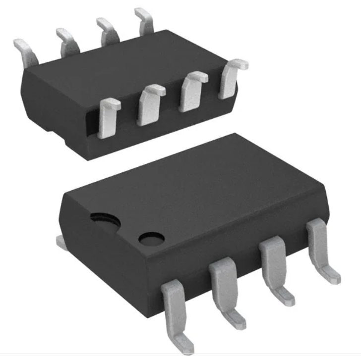
ACPL-T350
2.5 Amp Output Current IGBT Gate Driver Optocoupler with Low ICC
Data Sheet
Lead (Pb) Free
RoHS 6 fully
compliant
RoHS 6 fully compliant options available;
-xxxE denotes a lead-free product
Description
Features
The ACPL-T350 contains a GaAsP LED. The LED is optically
coupled to an integrated circuit with a power output
stage. These optocouplers are ideally suited for driving
power IGBTs and MOSFETs used in motor control inverter
applications. The high operating voltage range of the
output stage provides the drive voltages required by
gate controlled devices. The voltage and current supplied
by these optocouplers make them ideally suited for
directly driving IGBTs with ratings up to 1200 V/100 A.
For IGBTs with higher ratings, the ACPL-T350 series can
be used to drive a discrete power stage whichs drives the
IGBT gate. The ACPL-T350 has an insulation voltage of
VIORM = 630 Vpeak (Option 060).
2.5A Absolute Maximum Peak Output Current
Functional Diagram
ACPL-T350
8 VCC
N/C 1
ANODE 2
7 VO
CATHODE 3
6 VO
N/C 4
SHIELD
15 kV/μs minimum Common Mode Rejection (CMR) at
VCM = 1500 V
1.5 V maximum low level output voltage (VOL)
ICC = 4 mA maximum supply current
Under Voltage Lock-Out protection (UVLO) with
hysteresis
Wide operating VCC range: 15 to 30 Volts
500 ns maximum switching speeds
Industrial temperature range: -40°C to 100°C
Safety Approval
- UL Recognized 3750 Vrms for 1 min.
- CSA Approval
- IEC/EN/DIN EN 60747-5-5 Approved
VIORM = 630 Vpeak (Option 060)
Applications
IGBT/MOSFET gate drive
Inverter for Home Appliances
Industrial Inverters
5 VEE
Switching Power Supplies (SPS)
Note: A 0.1 μF bypass capacitor must be connected between pins VCC
and VEE.
UVLO Truth Table
LED
VCC – VEE
“POSITIVE GOING”
(i.e., TURN-ON)
VCC – VEE
“NEGATIVE GOING”
(i.e., TURN-OFF)
VO
OFF
0 - 30 V
0 - 30 V
LOW
ON
0 - 11 V
0 - 9.5 V
LOW
ON
11 - 13.5 V
9.5 - 12 V
TRANSITION
ON
13.5 - 30 V
12 - 30 V
HIGH
CAUTION: It is advised that normal static precautions be taken in handling and assembly
of this component to prevent damage and/or degradation which may be induced by ESD.
�Ordering Information
ACPL-T350 is UL Recognized with 3750 Vrms for 1 minute per UL1577.
Part
number
ACPL-T350
Option
RoHS Compliant
Package
Surface Mount
Gull Wing
-300E
-000E
300mil DIP-8
X
X
-500E/500ME
X
X
Tape& Reel
IEC/EN/DIN EN
60747-5-5
Quantity
50 per tube
50 per tube
X
-060E
1000 per reel
X
-360E
X
X
-560E/560ME
X
X
X
50 per tube
X
50 per tube
X
1000 per reel
To order, choose a part number from the part number column and combine with the desired option from the option
column to form an order entry.
Example 1:
ACPL-T350-560E to order product of 300mil DIP Gull Wing Surface Mount package in Tape and Reel packaging with
IEC/EN/DIN EN 60747-5-5 Safety Approval in RoHS compliant.
Example 2:
ACPL-T350-000E to order product of 300mil DIP package in tube packaging and RoHS compliant.
Option datasheets are available. Contact your Avago sales representative or authorized distributor for information.
Remarks: The notation ‘#XXX’ is used for existing products, while (new) products launched since 15th July 2001 and
RoHS compliant option will use ‘-XXXE‘.
Regulatory Information
The ACPL-T350 is approved by the following organizations:
IEC/EN/DIN EN 60747-5-5 (ACPL-T350 Option 060 only)
UL
Approval under:
DIN EN 60747-5-5 (VDE 0884-5):2011-11
EN 60747-5-5:2011
Approval under UL 1577, component recognition
program, File E55361.
CSA
Approval under CSA Component Acceptance Notice #5,
File CA 88324.
Recommended Pb-Free IR Profile
Recommended reflow condition as per JEDEC Standard, J-STD-020 (latest revision). Non-Halide Flux should be used.
2
�Package Outline Drawings
ACPL-T350 Outline Drawing
7.62 – 0.25
(0.300 – 0.010)
9.65 – 0.25
(0.380 – 0.010)
8
TYPE NUMBER
7
6
5
6.35 – 0.25
(0.250 – 0.010)
OPTION CODE*
DATE CODE
A XXXXZ
YYWW
1
2
3
4
1.78 (0.070) MAX.
1.19 (0.047) MAX.
+ 0.076
0.254 - 0.051
+ 0.003)
(0.010 - 0.002)
5° TYP.
3.56 – 0.13
(0.140 – 0.005)
4.70 (0.185) MAX.
0.51 (0.020) MIN.
2.92 (0.115) MIN.
DIMENSIONS IN MILLIMETERS AND (INCHES).
* MARKING CODE LETTER FOR OPTION NUMBERS.
"V" = OPTION 060
OPTION NUMBERS 300 AND 500 NOT MARKED.
0.65 (0.025) MAX.
1.080 – 0.320
(0.043 – 0.013)
2.54 – 0.25
(0.100 – 0.010)
NOTE: FLOATING LEAD PROTRUSION IS 0.25 mm (10 mils) MAX.
ACPL-T350 Outline Drawing
LAND PATTERN RECOMMENDATION
9.65 – 0.25
(0.380 – 0.010)
8
7
6
1.016 (0.040)
5
6.350 – 0.25
(0.250 – 0.010)
1
2
3
10.9 (0.430)
4
1.27 (0.050)
9.65 – 0.25
(0.380 – 0.010)
1.780
(0.070)
MAX.
1.19
(0.047)
MAX.
7.62 – 0.25
(0.300 – 0.010)
3.56 – 0.13
(0.140 – 0.005)
1.080 – 0.320
(0.043 – 0.013)
0.635 – 0.25
(0.025 – 0.010)
2.54
(0.100)
BSC
0.635 – 0.130
(0.025 – 0.005)
DIMENSIONS IN MILLIMETERS (INCHES).
LEAD COPLANARITY = 0.10 mm (0.004 INCHES).
NOTE: FLOATING LEAD PROTRUSION IS 0.25 mm (10 mils) MAX.
3
2.0 (0.080)
+ 0.076
0.254 - 0.051
+ 0.003)
(0.010 - 0.002)
12° NOM.
�Table 1. IEC/EN/DIN EN 60747-5-5 Insulation Characteristics* (ACPL-T350 Option 060)
Description
ACPL-T350
Option 060
Symbol
Installation classification per DIN VDE 0110/39, Table 1
for rated mains voltage ≤ 150 Vrms
for rated mains voltage ≤ 300 Vrms
for rated mains voltage ≤ 450 Vrms
I – IV
I – IV
I – III
Climatic Classification
55/100/21
Pollution Degree (DIN VDE 0110/39)
Unit
2
Maximum Working Insulation Voltage
VIORM
630
Vpeak
Input to Output Test Voltage, Method b*
VIORM x 1.875=VPR, 100% Production Test with tm=1 sec, Partial discharge < 5 pC
VPR
1181
Vpeak
Input to Output Test Voltage, Method a*
VIORM x 1.6=VPR, Type and Sample Test, tm=10 sec, Partial discharge < 5 pC
VPR
1008
Vpeak
Highest Allowable Overvoltage (Transient Overvoltage tini = 60 sec)
VIOTM
6000
Vpeak
Case Temperature
TS
175
°C
Input Current
IS, INPUT
230
mA
Output Power
PS, OUTPUT
600
mW
Insulation Resistance at TS, VIO = 500 V
RS
>109
* Refer to the optocoupler section of the Isolation and Control Components Designer’s
Catalog, under Product Safety Regulations section, (IEC/EN/DIN EN 60747-5-5) for a
detailed description of Method a and Method b partial discharge test profiles.
Note: These optocouplers are suitable for “safe electrical isolation” only within the safety
limit data. Maintenance of the safety data shall be ensured by means of protective circuits.
Surface mount classification is Class A in accordance with CECC 00802.
OUTPUT POWER - PS, INPUT CURRENT - IS
Safety-limiting values – maximum values allowed in the event of a failure
ACPL-T350 Option 060
1000
PS (mW)
IS (mA)
800
600
400
200
0
0
25
50
75 100 125
TS - CASE TEMPERATURE - qC
150
175
Table 2. Insulation and Safety Related Specifications
Parameter
Symbol
ACPL-T350 Units
Conditions
Minimum External Air
Gap (Clearance)
L(101)
7.1
mm
Measured from input terminals to output terminals, shortest distance
through air.
Minimum External
Tracking (Creepage)
L(102)
7.4
mm
Measured from input terminals to output terminals, shortest distance
path along body.
0.08
mm
Through insulation distance conductor to conductor, usually the
straight line distance thickness between the emitter and detector.
> 175
V
DIN IEC 112/VDE 0303 Part 1
Minimum Internal
Plastic Gap
(Internal Clearance)
Tracking Resistance
(Comparative Tracking
Index)
Isolation Group
CTI
IIIa
Material Group (DIN VDE 0110, 1/89, Table 1)
All Avago data sheets report the creepage and clearance inherent to the optocoupler component itself. These dimensions are needed as a starting
point for the equipment designer when determining the circuit insulation requirements. However, once mounted on a printed circuit board,
minimum creepage and clearance requirements must be met as specified for individual equipment standards. For creepage, the shortest distance
path along the surface of a printed circuit board between the solder fillets of the input and output leads must be considered (the recommended
Land Pattern does not necessarily meet the minimum creepage of the device). There are recommended techniques such as grooves and ribs which
may be used on a printed circuit board to achieve desired creepage and clearances. Creepage and clearance distances will also change depending
on factors such as pollution degree and insulation level.
4
�Table 3. Absolute Maximum Ratings
Parameter
Symbol
Min.
Max.
Units
Storage Temperature
TS
-55
125
°C
Operating Temperature
TA
-40
100
°C
Note
Average Input Current
IF(AVG)
25
mA
Peak Transient Input Current
( 5 V
Threshold Input Voltage
High to Low
VFHL
0.8
V
IO = 0 mA, VO > 5 V
Input Forward Voltage
VF
1.2
V
IF = 10 mA
Temperature Coefficient
of Input Forward Voltage
VF/TA
mV/°C
IF = 10 mA
Input Reverse
Breakdown Voltage
BVR
V
IR = 10 μA
Input Capacitance
CIN
pF
f = 1 MHz, VF = 0 V
UVLO Threshold
VUVLO+
11.0
V
IF = 10 mA, VO > 5 V 14, 20
VUVLO–
9.5
UVLO Hysteresis
1.5
1.8
-2.0
5
60
12.3
13.5
10.7
12.0
1.6
UVLOHYS
V
IF = 10 mA, VO > 5 V
V
IF = 10 mA, VO > 5 V
5
2
6, 7
9, 19
Table 6. Switching Specifications (AC)
Over recommended operating conditions (TA = -40 to 100°C, IF(ON) = 7 to 16 mA, VF(OFF) = -3.6 to 0.8 V, VCC = 15 to 30
V, VEE = Ground) unless otherwise specified. All typical values at TA = 25°C and VCC - VEE = 30 V, unless otherwise noted.
Parameter
Symbol
Min.
Typ.
Max.
Units
Test Conditions
Fig.
Note
Propagation Delay Time
to High Output Level
tPLH
0.05
0.25
0.5
μs
10, 11,
12, 21
8
Propagation Delay Time
to Low Output Level
tPHL
0.05
0.25
0.5
μs
Rg = 10 , Cg = 10 nF,
f = 10 kHz,
Duty Cycle = 50%
Pulse Width Distortion
PWD
0.3
μs
9
Propagation Delay Difference
Between Any Two Parts or
Channels
PDD
(tPHL – tPLH)
0.35
μs
10
Rise Time
tR
15
ns
Fall Time
tF
20
ns
Output High Level Common
Mode Transient Immunity
|CMH|
15
20
kV/μs
TA = 25°C,
IF = 10 to 16 mA,
VCM = 1500 V,
VCC = 30 V
22
11, 12
Output Low Level Common
Mode Transient Immunity
|CML|
15
20
kV/μs
TA = 25°C, VF = 0 V,
VCM = 1500 V ,
VCC = 30 V
22
11, 13
6
-0.35
21
�Table 7. Package Characteristics
Over recommended temperature (TA = -40 to 100°C) unless otherwise specified. All typicals at TA = 25°C.
Parameter
Symbol
Min.
Input-Output Momentary Withstand
Voltage**
VISO
3750
Resistance Input-Output)
RI-O
Capacitance Input-Output)
Typ.
Max.
Units
Test Conditions
Fig.
Note
Vrms
RH < 50%,
t = 1 min.,
TA = 25°C
14, 15
1012
VI-O = 500 V
15
CI-O
0.6
pF
Freq=1 MHz
LED-to-Case Thermal Resistance
LC
467
°C/W
LED-to-Detector Thermal Resistance
LD
442
°C/W
Detector-to-Case Thermal Resistance
DC
126
°C/W
Thermocouple located
at center underside of
package
** The Input-Output Momentary Withstand Voltage is a dielectric voltage rating that should not be interpreted as an input-output continuous
voltage rating. For the continuous voltage rating refers to your equipment level safety specification or Avago Application Note 1074 entitled
“Optocoupler Input-Output Endurance Voltage.”
Notes:
1. Derate linearly above 70°C free-air temperature at a rate of 0.3 mA /°C.
2. Maximum pulse width = 10 μs.
3. Derate linearly above 70° C free-air temperature at a rate of 4.8 mW /°C.
4. Derate linearly above 70° C free-air temperature at a rate of 5.4 mW /°C. The maximum LED junction temperature should not exceed 125°C.
5. Maximum pulse width = 50 μs
6. In this test VOH is measured with a dc load current. When driving capacitive loads VOH will approach VCC as IOH approaches zero amps.
7. Maximum pulse width = 1 ms
8. This load condition approximates the gate load of a 1200 V/100A IGBT.
9. Pulse Width Distortion (PWD) is defined as |tPHL - tPLH| for any given device.
10. The difference between tPHL and tPLH between any two ACPL-T350 parts under the same test condition.
11. Pins 1 and 4 need to be connected to LED common.
12. Common mode transient immunity in the high state is the maximum tolerable dVCM/dt of the common mode pulse, VCM, to assure that the
output will remain in the high state (i.e., VO > 15.0 V).
13. Common mode transient immunity in a low state is the maximum tolerable dVCM/dt of the common mode pulse, VCM, to assure that the output
will remain in a low state (i.e., VO < 2.0 V).
14. In accordance with UL1577, each optocoupler is proof tested by applying an insulation test voltage ≥ 4500 Vrms for 1 second (leakage detection
current limit, II-O ≤ 5 μA).
15. Device considered a two-terminal device: pins 1, 2, 3, and 4 shorted together and pins 5, 6, 7, and 8 shorted together.
7
�-3
-4
-40 -20
0
20
40
60
80
100
1.6
1.4
1.2
1.0
-40 -20
TA - TEMPERATURE - ° C
IOL - OUTPUT LOW CURRENT - A
VOL - OUTPUT LOW VOLTAGE - V
0.15
0.10
0.05
-20
0
20
40
60
80
100
100
80
-2
-3
-4
100 ° C
25 ° C
-40 ° C
-5
-6
0
4
VF (OFF) = -3.0 TO 0.8 V
VOUT = 2.5 V
VCC = 15 TO 30 V
VEE = 0 V
3
2
1
0
-40
-20
0
20
40
60
80
100
1.50
--------- I CcH
I CCL
1.00
-40 -20 0
20 40 60 80 100
TA - TEMPERATURE - oC
Icc - SUPPLY CURRENT - mA
2.00
2.00
1.50
--------- I CcH
I CCL
20
25
Vcc - SUPPLY VOLTAGE - V
Figure 8. ICC vs. VCC
1.5
2.0
2.5
VF(OFF) = -3.0 to 0.8 V
VCC = 15 to 30 V
VEE = 0 V
3
2
1
0
100 ° C
25 ° C
-40 ° C
0
0.5
Figure 6. VOL vs. IOL.
2.50
1.00
15
1.0
1.0
1.5
2.0
IOL - OUTPUT LOW CURRENT - A
3.00
2.50
0.5
Figure 3. VOH vs. IOH.
Figure 5. IOL vs. temperature.
3.00
Figure 7. ICC vs. Temperature
IF = 7 to 16 mA
VCC = 15 to 30 V
VEE = 0 V
IOH - OUTPUT HIGH CURRENT - A
TA - TEMPERATURE - ° C
Figure 4. VOL vs. temperature.
Icc - SUPPLY CURRENT - mA
60
4
VF (OFF) = -3.0 TO 0.8 V
IOUT = 100 mA
VCC = 15 TO 30 V
VEE = 0 V
TA - TEMPERATURE - ° C
8
40
Figure 2. IOH vs. temperature.
0.25
0
-40
20
-1
TA - TEMPERATURE - ° C
Figure 1. VOH vs. temperature.
0.20
0
(VOH - V CC ) - OUTPUT HIGH VOLTAGE DROP - V
-2
1.8
IF = 7 to 16 mA
VOUT = (VCC - 4 V)
VCC = 15 to 30 V
VEE = 0 V
VOL - OUTPUT LOW VOLTAGE - V
-1
2.0
IF = 7 to 16 mA
IOUT = -100 mA
VCC = 15 to 30 V
VEE = 0 V
IOH - OUTPUT HIGH CURRENT - A
(V OH - V CC ) - HIGH OUTPUT VOLTAGE DROP - V
0
30
2.5
�2
1
0
-40 -20
0
20
40
60
80
- - - - - - TpHL
TpLH
20
25
Vcc-SUPPLY VOLTAGE-V
1000
I F = 7mA
VCC =30V, VEE = 0V
400
Rg= 10Ω , Cg = 10nF
Duty Cycle = 50%, f = 10kHz
300
200
-------- TpHL
TpLH
100
-40
-20
0
20
40
60 80
TA - TEMPERATURE - oC
Figure 12. Propagation delay vs. Temperature
100
300
200
- - - - - - TpHL
TpLH
30
Figure 10. Propagation delay vs. VCC.
IF
1.0
0.1
0.01
1.20
1.30
1.40
8
9
10
11
12
13
14
15
IF - FORWARD LED CURRENT - mA
14
TA = 25° C
10
0.001
1.10
7
Figure 11. Propagation delay vs. IF.
+
VF
-
100
VCC =30V, VEE =0V
Rg= 10Ω, Cg = 10nF
Duty = 50% f = 10kHz
TA= 25 o C
400
100
100
15
IF - FORWARD CURRENT - mA
Tp - PROPAGATION DELAY - ms
200
TA - TEMPERATURE - ° C
500
9
300
100
Figure 9. IFLH vs. temperature.
Tp - PROPAGATION DELAY - ms
3
400
500
I F =7mA, TA =25 o C
Rg = 10Ω, Cg = 10nF
Duty = 50% f = 10kHz
VO - OUTPUT VOLTAGE - V
4
VCC = 15 TO 30 V
VEE = 0 V
OUTPUT = OPEN
Tp - PROPAGATION DELAY - ms
I FLH - LOW TO HIGH CURRENT THRESHOLD - mA
500
5
1.50
1.60
VF - FORWARD VOLTAGE - VOLTS
Figure 13. Input current vs. forward voltage.
12
(12.3, 10.8)
10
(10.7, 9.2)
8
6
4
2
0
(10.7, 0.1)
0
5
10
(12.3, 0.1)
15
20
(VCC - VEE ) - SUPPLY VOLTAGE - V
Figure 14. Under voltage lock out.
16
�1
8
0.1
2
F
+
-
7
IF = 7 to
16 mA
4V
+ VCC = 15
to 30 V
3
6
IOH
4
5
Figure 15. IOH test circuit.
1
8
2
7
0.1
3
F
8
2
7
0.1
IOL
+ VCC = 15
to 30 V
F
VOH
IF = 7 to
16 mA
+ VCC = 15
to 30 V
2.5 V +
-
6
1
6
3
100 mA
4
5
4
Figure 17. VOH Test circuit.
Figure 16. IOL Test circuit.
1
8
0.1
2
F
3
6
4
5
10
1
8
2
7
0.1
100 mA
7
+ VCC = 15
to 30 V
Figure 18. VOL Test circuit.
5
VOL
IF
3
6
4
5
Figure 19. IFLH Test circuit.
F
VO > 5 V
+ VCC = 15
to 30 V
�1
8
2
7
0.1
IF = 10 mA
3
6
4
5
F
+
-
VO > 5 V
VCC
Figure 20. UVLO Test Circuit
1
8
0.1
IF = 7 to 16 mA
+
10 KHz -
500 Ω
50% DUTY
CYCLE
2
F
7
IF
VCC = 15
+ to
30 V
-
tr
tf
VO
6
3
90%
10 Ω
50%
VOUT
10 nF
4
10%
5
tPLH
tPHL
Figure 21. tPLH, tPHL, tr, and tf test circuit and waveforms.
VCM
5V
0.1
A
B
V
8
1
IF
2
t
F
VO
3
6
4
5
VCC = 30 V
VO
-
Figure 22. CMR test circuit and waveforms.
11
VOH
SWITCH AT A: IF = 10 mA
SWITCH AT B: IF = 0 mA
+
t
t
+
-
VO
VCM = 1500 V
VCM
0V
7
+
-
=
VOL
�Typical Application Circuit
ACPL-T350
+5 V
8
1
270 Ω
0.1
2
F
+
-
VCC = 18 V
+ HVDC
7
Rg
CONTROL
INPUT
74XXX
OPEN
COLLECTOR
3
6
4
5
Q1
3-PHASE
AC
Q2
- HVDC
Figure 23. Recommended LED drive and application circuit.
ACPL-T350
+5 V
1
270 Ω
8
0.1
2
F
+
-
VCC = 15 V
+ HVDC
7
Rg
CONTROL
INPUT
74XXX
OPEN
COLLECTOR
3
Q1
6
+
-
4
VEE = -5 V
3-PHASE
AC
5
Q2
Figure 24. Typical application circuit with negative IGBT gate drive.
For product information and a complete list of distributors, please go to our web site:
www.avagotech.com
Avago, Avago Technologies, and the A logo are trademarks of Avago Technologies, Limited in the United States and other countries.
Data subject to change. Copyright © 2012-2016 Avago Technologies Limited. All rights reserved.
AV02-0308EN - September 23, 2016
- HVDC
��


 工商网监
湘ICP备2023018690号
工商网监
湘ICP备2023018690号
