Data Sheet
AFBR-3905xxRZ
High-Voltage Galvanic Insulation Link
for DC to 5 Mbaud
Description
Features
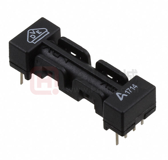
The Broadcom® AFBR-3905xxZ is a high-voltage galvanic
insulation link for DC to 5 Mbaud. The AFBR-3905xxZ
consists of an optical transmitter and receiver operating at a
wavelength of 650 nm. A pin-to-pin distance of
approximately 25 mm to 101 mm provides transient voltage
suppression in the range of 15 kV to 50 kV.
Applications
Drives/inverters
Galvanic insulation on one single PCB
Medium voltage power distributions
Regulated distribution transformers
Smart grid onboard insulations
Data transmission at signal rates of DC to 5 Mbaud
DC-coupled receiver with CMOS/TTL output for easy
designs: no data encoding or digitizing circuitry required
High noise immunity through the receiver IC with
integrated photodiode
RoHS compliant
Transient voltage suppression in the range of 15 kV to
50 kV according to IEC 60644
Laser class 1 according to IEC-60825
Certified according to IEC-60747-5-5
Housing Material UL-V0 with CTI ≥ 600
Optional 3.3V or 5V power supply
Ordering Information
Part Number
Length
mm
Voltage
Suppression
AFBR-390525RZ
1 inch
25
15 kV
AFBR-390550RZ
2 inch
50.4
27 kV
AFBR-390575RZ
3 inch
75.8
40 kV
AFBR-390500RZ
4 inch
101.2
50 kV
Broadcom
AV02-4872EN
May 31, 2023
�AFBR-3905xxRZ Data Sheet
High-Voltage Galvanic Insulation Link for DC to 5 Mbaud
Absolute Maximum Ratings
Parameter
Symbol
Min.
Max.
Units
fs
DC
5
Mbaud
Storage and Operating Temperature
TS,O
–40
+85
°C
Receiver Supply Voltage
VDD
–0.5
+5.5
V
Receiver Output Current
IOAV
—
10
mA
Transmitter Peak Forward Input Current
IF,PK
—
30
mA
VR
—
3
V
Temp
TSOL
—
+260
°C
Time
—
—
10
sec
Signaling Rate
Transmitter Reverse Input Voltage
Lead Soldering Cycle a, b
a. 1.6 mm below the seating plane; wave soldering only. To guard against solder process fluctuations, the recommended nominal soldering time
is 5 seconds.
b. MSL class 3.
ATTENTION: Stresses above those listed here may cause permanent damage to the device. Exposure to absolute
maximum rating conditions for extended periods may affect device reliability.
Recommended Operating Conditions
Parameter
Ambient Temperature
Symbol
Min.
Max.
Units
TA
–40
85
°C
3.135
3.465
V
4.75
5.25
V
Rx Power Supply Voltage a
VCC
Transmitter Average Forward Current
IF,AV
5
10
mA
fs
DC
5
Mbaud
Signaling Rate
a. < 100 mVpp of noise.
ATTENTION: All the data in this specification refers to the operating conditions above and over lifetime unless otherwise
stated.
Broadcom
AV02-4872EN
2
�AFBR-3905xxRZ Data Sheet
High-Voltage Galvanic Insulation Link for DC to 5 Mbaud
Insulation Characteristics
Parameter
Apparent charge at Sample Test stage and Type Test stage after
subgroup 1 (method a)
a
Apparent charge at Routine Test stage and Type Test stage,
Preconditioning (method b)
b
Maximum Transient Voltage, peak c
Maximum Transient Voltage, effective c
Maximum Working Voltage, peak d
Maximum Working Voltage, effective d
Insulation Resistance @ Tamb,max, min. 100°C
Insulation Resistance @ TS
Creepage Distance
Clearance Distance
Surge Isolation Voltage
Comparative Tracking Index
Symbol
Min.
Max.
Units
qpd
—
5
pC
qpd
—
5
pC
VIOTM_1inch
VIOTM_2inch
VIOTM_3inch
VIOTM_4inch
VISO_1inch
VISO_2inch
VISO_3inch
VISO_4inch
VIORM_1inch
VIORM_2inch
VIORM_3inch
VIORM_4inch
VIOWM_1inch
VIOWM_2inch
VIOWM_3inch
VIOWM_4inch
RIO
15
27
40
50
10.5
19
28.1
35.2
4.25
8.5
12.75
17.00
3
6
9
12
—
kV
—
kV
—
kV
—
kV
—
Ω
RIO
1inch
2inch
3inch
4inch
1inch
2inch
3inch
4inch
VIOSM
CTI
1011
9
—
Ω
—
mm
10
25
50.4
75.8
101.2
25
50.4
75.8
101.2
12
—
mm
—
kV
600
—
—
Pollution Degree e
—
2
—
—
Climatic Category
Maximum Ambient Safety Temperature
—
40/085/21
—
—
TS
f
Maximum Input Current
Maximum Output Current
Maximum Input Power Dissipation
Maximum Output Power Dissipation
110
—
°C
ISI
60
—
mA
30
—
mA
PSI
330
—
mW
165
—
mW
ISO
PSO
a. Vpd(m) = 1.6 × VIORM (= 6.8 kV for 1inch, = 13.6 kV for 2inch, = 20.4 kV for 3inch, = 27.2 kV for 4inch), Vini,a = VIOTM, tini,a = 60s; tm = 10s.
b. Vpd(m) = 1.875 × VIORM (= 8 kV for 1inch, = 16 kV for 2inch, = 24 kV for 3inch, = 32 kV for 4inch), Vini,b = VIOTM, tini,b = 1s; tm = 1s.
c. Altitude up to 2000m above sea level.
d. Pollution degree 2; please note that inhomogeneous field conditions may lead to partial discharge through air for these voltages.
e. According to IEC-60664-1.
f. According to IEC-60068-1.
Broadcom
AV02-4872EN
3
�AFBR-3905xxRZ Data Sheet
High-Voltage Galvanic Insulation Link for DC to 5 Mbaud
Electrical Input Characteristics
Parameter
Symbol
Min.
Typ.
Max.
Units
VF
1.6
—
2.2
V
ΔVF /ΔT
—
–1.8
—
mV/°C
VBR
3.0
13
—
V
C0
—
30
—
pF
Forward Voltage a
Forward Voltage Temperature Coefficient
Reverse Input Breakdown Voltage
Diode Capacitance
b
c
a. IF,dc = 10 mA
b. IF,dc = –10 µA
c. VF = 0V; f = 1 MHz
Electrical Output Signal Characteristics
Parameter
Symbol
Min.
Typ.
Max.
Units
High Level Output Voltage
VOH
2.5
VCC
VCC + 0.3
V
Low Level Output Voltage
VOL
—
0.22
0.4
V
Output Risetime (10–90%) a, b
tr
—
—
10
ns
Output Falltime (90–10%) a, b
tf
—
—
10
ns
Power Supply Noise Immunity c
PSNI
0.1
0.4
—
Vpp
Vcc Level to Deactivate POR d
VPOR_DEACT
—
2.8
—
V
VPOR_ACT
—
2.6
—
V
tPOR-DEACT_DEL
—
100
—
µs
Vcc Level to Activate POR d
POR Deactivate Delay Time
d
a. CL = 20 pF, RL = 50 kΩ.
b. In the recommended drive circuit.
c. Peak-to-peak sine wave.
d. Power-on reset (POR) is active below VPOR_DEACT. Once VPOR_DEACT is reached, the POR remains active for tPOR-DEACT_DEL. During
power-down, the POR starts at VPOR_ACT.
Figure 1: Typical Power-On Reset Functionality
Data_In
(optical)
time
VPOR_DEACT
V CC
VPOR_ACT
POR disabled at ~ 2.8V
POR enabled at ~ 2.6V
~100μs
delay
time
Data_Out
Data_Out = Inverted Data_In (optical)
Broadcom
time
AV02-4872EN
4
�AFBR-3905xxRZ Data Sheet
High-Voltage Galvanic Insulation Link for DC to 5 Mbaud
Specified Link Performance
TA = –40°C to +85°C, DC to 5 Mbaud, unless otherwise noted.
Parameter
Symbol
Min.
Typ.
Max.
Unit
Condition
fS
DC
—
5
Mbaud
NRZ
PWD
–30
—
30
ns
5 Mbaud
Propagation Delay b
tD
—
—
80
ns
5 Mbaud
Skew c
tS
—
—
20
ns
5 Mbaud
ICC
—
6
10
mA
—
Signaling Rate
Pulse Width Distortion a
Supply Current Rx d
a. ±15% of the nominal pulse width, provided no pulse width distortion at the electrical input.
b. Determined from 50% of the rising edge of data_in to 50% of the consecutive rising edge of data_out.
c. Variations of tD between multiple devices measured for the same input conditions and the same external signal delay.
d. CL = 20 pF, RL = 50 kΩ.
Block Diagram – AFBR-3905xxRZ
RX
TX
PD Filter
& Monitor
Anode
VCC
Power on
reset
LED
Rod
TIA2
Output
driver
Data_out
TIA1
Cathode
Gain Control
etc.
VSS
(GND)
The Rx Data_out signal is inverted, which means that light_on will lead to Data_out low.
The POR remains active during VCC power-up, typically until 100 µs after 2.8V is reached. The POR follows VCC while active.
Recommended Chemicals for Cleaning and Degreasing
Alcohols: methyl, isopropyl, isobutyl
Aliphatics: hexane, heptanes
Other: soap solution, naphtha
Do not use partially halogenated hydrocarbons, such as 1,1,1 trichloroethane, or ketones, such as MEK, acetone,
chloroform, ethyl acetate, methylene dichloride, phenol, methylene chloride, or N-methylpyrolldone. Also, Broadcom does
not recommend the use of cleaners that use halogenated hydrocarbons because of their potential environmental harm.
Broadcom
AV02-4872EN
5
�AFBR-3905xxRZ Data Sheet
High-Voltage Galvanic Insulation Link for DC to 5 Mbaud
Recommended Drive Circuit (a) – Top View
V CC Tx
R1
6
R2
8
C1
C2
Tx
Value
Tolerance
R1
4.7kΩ
5%
R2
390Ω
1%
C1
0.1μF
20%
C2
1.0μF
20%
V CC Rx
C3
1
2
3
4
5
5
6
7
8
Data_IN
7
Rx
Value
Tolerance
C3
0.1μF
20%
Data_out
1/2 SN75451
4
Recommended Drive Circuit (b) – Top View
V CC Rx
V CC Tx
R3
Data_in
R1
Broadcom
C2
C3
Rx
Value
Tolerance
C3
0.1μF
20%
1
2
3
4
2N7002E
R2
C1
R4
5
6
7
8
Tx
Value
Tolerance
R1
47Ω
5%
R2
1kΩ
5%
R3
390Ohm
2%
R4
150Ohm
2%
C1
0.1μF
20%
C2
1.0μF
20%
Data_out
AV02-4872EN
6
�AFBR-3905xxRZ Data Sheet
High-Voltage Galvanic Insulation Link for DC to 5 Mbaud
Pin Description
Pin Number
Transmitter
Pin Number
Receiver
1
Anode
5
No function a
2
Cathode
6
VCC
3
No function
a
7
GND
4
No function a
8
Data_out
a. It is recommended to connect this pin to signal ground.
Pinning Schematic
Broadcom
AV02-4872EN
7
�AFBR-3905xxRZ Data Sheet
High-Voltage Galvanic Insulation Link for DC to 5 Mbaud
Footprint (Top View)
Dimensions are in mm.
AFBR-390525RZ
22.08
1.14 (4x)
2.54 (3x)
2.54
0.5 (8x)
)
(2x
1.6
7.62
10.04
0.38 (8x)
20.32
25.4
AFBR-390550RZ
47.48
1.14 (4x)
2.54
0.5 (8x)
)
(2x
1.6
2.54 (3x)
7.62
10.04
0.38 (8x)
45.72
50.8
Broadcom
AV02-4872EN
8
�AFBR-3905xxRZ Data Sheet
High-Voltage Galvanic Insulation Link for DC to 5 Mbaud
AFBR-390575RZ
72.88
1.14 (4x)
2.54 (3x)
2.54
0.5 (8x)
(2x)
1.6
7.62
10.04
0.38 (8x)
71.12
76.2
AFBR-390500RZ
98.28
1.14 (4x)
2.54
0.5 (8x)
7.62
)
(2x
1.6
2.54 (3x)
10.04
0.38 (8x)
96.52
101.6
Broadcom
AV02-4872EN
9
�AFBR-3905xxRZ Data Sheet
High-Voltage Galvanic Insulation Link for DC to 5 Mbaud
Mechanical Dimensions
Dimensions are in mm.
AFBR-390525RZ
1.
6
(2
x)
2.54
20.32
30.46
2.5
7.7
11.49
6.7
10.16
25.4
2.54
0.38
7.62
AFBR-390550RZ
2.54
45.72
)
(2x
1.6
2.5
7.7
10.16
11.49
6.7
55.86
50.8
2.54
0.38
7.62
Broadcom
AV02-4872EN
10
�AFBR-3905xxRZ Data Sheet
High-Voltage Galvanic Insulation Link for DC to 5 Mbaud
AFBR-390575RZ
2.54
71.12
)
(2x
1.6
81.26
2.5
7.7
11.49
6.7
10.16
76.2
2.54
0.38
7.62
96.1
0.83
AFBR-390500RZ
6
1.
x)
(2
6.57
7.7
101.6
11.49
0.44
6.7
10.16
0.38
2.54
7.62
CAUTION! AFBR-3905xxRZ devices must not be bent under any circumstances.
Broadcom
AV02-4872EN
11
�Copyright © 2015–2023 Broadcom. All Rights Reserved. The term “Broadcom” refers to Broadcom Inc. and/or its
subsidiaries. For more information, go to www.broadcom.com. All trademarks, trade names, service marks, and logos
referenced herein belong to their respective companies.
Broadcom reserves the right to make changes without further notice to any products or data herein to improve reliability,
function, or design. Information furnished by Broadcom is believed to be accurate and reliable. However, Broadcom does
not assume any liability arising out of the application or use of this information, nor the application or use of any product or
circuit described herein, neither does it convey any license under its patent rights nor the rights of others.
�