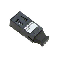
AFBR-5978Z
Digital Diagnostic 650nm Transceiver for Fast Ethernet (10/100 Mbps) with SC-RJ connector
Data Sheet
Description
The AFBR-5978Z transceiver provides the system designer with the ability to implement Fast Ethernet (100 Mbps) or Ethernet (10 Mbps) over 50 meter standard bandwidth 0.5±0.05 NA POF and 100 meter standard bandwidth 0.37±0.04 NA HCS fiber. The connectivity available for the transceiver is SC-RJ. This product is lead free and compliant with RoHS.
Features
• Compatible with electrical and optical performance of the POFAC recommendations for the Fast Ethernet over Plastic Optical Fiber (POF). • Compatible with the Electrical and Optical performance of the ProfiNet recommendations the Fast Ethernet over POF and Hard-Clad Silica Fiber (HCS). • Manufactured in an ISO 9001 certified facility • DMI [Digital Diagnostics Monitoring Interface, SFF-8472 Rev 9.3], provides real-time monitoring of: - Temperature - Supply voltage - Received Optical Power (Alarm/Warning flag) • LVPECL Signal Detect Output • Temperature range –25 to +85 °C
Transmitter
The transmitter contains a 650nm LED with an integrated driver. The LED driver operates at 3.3 V. It receives a LVPECL compatible electrical input, and converts it into a modulated current driving the LED. The LED is packaged in an optical subassembly, part of the transmitter section. The optical subassembly couples the output optical power efficiently into POF or HCS fiber.
Receiver
The receiver utilizes a Si PIN photodiode. The PIN photodiode is packaged in an optical sub-assembly, part of the receiver section. This optical subassembly couples the optical power efficiently from POF or HCS fiber to the receiving PIN. The integrated IC operates at 3.3 V and converts the photocurrent into LVPECL compatible electrical output.
Applications
• Factory automation at Fast Ethernet speeds • Fast Ethernet networking over POF and HCS • Link Distance up to 50 m POF or 100 m HCS (See application note 5290 for details)
HCS® is a trademark of OFS Corporation AFBR-5978Z is compatible with the SC-RJ Connecting System from Reichle & De-Massari AG, Switzerland
Package
The transceiver package consist of four basic elements; two optical subassemblies, an electrical subassembly and the housing as illustrated in the block diagrams in Figure 1. The package outline drawing and pin out are shown in Figures 2 and 3.
�Block diagram
ELECTRICAL SUBASSEMBLY DIFFERENTIAL DATA OUT SINGLE-ENDED SIGNAL DETECT OUT QUANTIZER IC PREAMP IC OPTICAL SUBASSEMBLIES DMI DIFFERENTIAL DATA IN DRIVER IC SC-RJ RECEPTACLE PIN PHOTODIODE
LED
TOP VIEW Figure 1. Block diagram
The optical subassemblies utilize a high volume assembly process together with low cost lens elements which result in a cost effective building block. The electrical subassembly consists of a high volume multilayer printed circuit board on which the IC chips and various surface mounted passive circuit elements are attached. The housing includes internal shields for the electrical and optical subassemblies to insure low EMI emissions and high immunity to external EMI fields. The outer housing including the duplex SC-RJ connector is molded of filled non-conductive plastic to provide mechanical strength and electrical isolation. The low
profile of the Avago Technologies transceiver design complies with the maximum height allowed for the duplex SC-RJ connector over the entire length of the package. The transceiver is attached to a printed circuit board with twelve signal pins and the two solder posts, which exit the bottom of the housing. The two solder posts provide the primary mechanical strength to withstand the mechanical loads imposed on the transceiver by mating with the SC-RJ connectored fiber cables. The solder posts are isolated from the circuit design of the transceiver and do not require connection to a ground plane on the circuit board
Figure 2. Package outline drawing.
2
�Pin Descriptions
Pin 1 Sda: the data line of the two wire serial interface. This data line should be pulled up with a 4.7k–10kΩ resistor on the host board to a supply of 3.3V ±10%. Pin 2 Rx GND: receiver ground pin. Directly connect this pin to the receiver ground plane of the host board. Pin 3 Rx Vcc: receiver power supply pin. Provide +3.3 V DC via a receiver power supply filter circuit. Locate the power supply filter circuit as close as possible to the Vcc Rx pin. Pin 4 Sd: signal detect pin. If an optical signal is present at the input of the receiver, Sd output is a logic “1”. Absence of an optical signal to the receiver results in a logic “0” output. This signal detect output can be used to drive a LVPECL input on an upstream circuit, such as Signal Detect input or Loss of Signal–bar. Proper LVPECL termination should be in place. See figure 4. Pin 5 Rdata-: receiver data out bar. This data line is a 3.3V LVPECL compatible differential line which should be properly terminated with a 130Ω pull up to Vcc and 82Ω pull down to ground. Pin 6 Rdata+: receiver data out. This data line is a 3.3V LVPECL compatible differential line which should be properly terminated with a 130Ω pull up to Vcc and 82Ω pull down to ground. Pin 7 Tx Vcc: transmitter power supply. Provide +3.3V DC via a transmitter power supply filter circuit. Locate the power supply filter circuit as close as possible to the Vcc Tx pin. Pin 8 Tx GND: transmitter ground. Directly connect this pin to the transmitter ground plane on the host board. Pin 9 Txdis: transmitter disable input. This input is used to shut down the transmitter light output. It is internally pulled up with a ~8 kΩ resistor. Low (0-0.8 V) - transmitter on Between (0.8-2.0 V) - undefined High (2.0-3.63 V) – transmitter off Open – transmitter off Pin 10 Tdata+: transmitter data in. This data line is an AC coupled 100Ω differential line which does not need any termination at the user SERDES. The AC coupling is done inside the module and therefore not required on the host board. Pin 11 Tdata-: transmitter data in bar. This data line is an AC coupled 100Ω differential line which does not need any termination at the user SERDES. The AC coupling is done inside the module and therefore not required on the host board. Pin 12 Scl: the clock line of the two wire serial interface. This data line should be pulled up with a 4.7k – 10 kΩ resistor on the host board to a supply of 3.3V ±10%.
SC-RJ connector
Scl TdataTdata+ Txdis TxGND TxVcc
Sda RxGND RxVcc Sd RdataRdata+
bottom view
Figure 3. Pin Out diagram
3
�V cc 3.3V 10µF 0.1µF
1µH 0.1µ F
1µH
Protocol IC & SERDES
Tx disable TD+ TDV cc 3.3V 130 130 Z = 50 Ω Z = 50 Ω 82 82 10µF 0.1µF Z = 50 Ω Z = 50 Ω
Txdis
10nF
TxVcc
AFBR-5978Z
Tdata+
100
LED driver
10nF
RD+ RD-
Tdata-
RxVcc Rdata+ RdataSd Amplifier & Quantisizer
PC Master Signal Detect
82 4.7k-10k 4.7k-10k V cc 3.3V 130 V cc 3.3V
Sda Scl
EEPROM
Figure 4. Recommended termination circuit.
Board Layout – Decoupling Circuit and Ground Planes
It is important to take care in the layout of your circuit board to achieve optimum performance from the transceiver. A power supply decoupling circuit is recommended to filter out noise to assure optimal product performance. It is further recommended that a contiguous ground plane be provided in the circuit board directly under the transceiver to provide a low inductance ground for signal return current. This recommendation is in keeping with good high frequency board layout practices.
Functional Data I/O
The LVPECL receiver output of the Avago Technologies transceiver can be DC-coupled to the LVPECL compliant network interface through a Thèvenin equivalent transformation. For a 3.3V power supply the LVPECL outputs should be pulled up to Vcc with a 130Ω resistor and pulled down to ground with an 82Ω resistor. Both coupling resistors are preferably placed close to the network interface IC, see figure 4. AC-coupling can be used for systems in which the transceiver and connected logic are at different supply voltages. For AC coupling, the coupling capacitor should be large enough to avoid excessive low-frequency droop when the data signal contains long strings of consecutive identical digits. The LVPECL outputs have to be pulled down to ground first to DC bias the output before AC coupling. Because the LVPECL output common-mode voltage is fixed at Vcc – 1.3V, the DC-biasing resistor can be selected by assuming 14 mA DC current. This results in a bias-resistor value of 142Ω - 200Ω. After the AC-coupling capacitors, a Thèvenin equivalent transformation connects to the LVPECL compatible network interface, equal to the one used in DCcoupling.
4
�Digital Diagnostics Monitoring Interface
The AFBR-5978Z transceiver features an enhanced digital diagnostic interface, compliant to the “Digital Diagnostic Monitoring Interface for Optical Transceivers” SFF-8472 Multi-source Agreement (MSA). Please refer to the MSA document to access information on the range of options, both hardware and software, available to the host system for exploiting the available digital diagnostic features. The enhanced digital interface allows real-time access to device operating parameters, and includes optional digital features such as soft control and monitoring of I/O signals. In addition, it fully incorporates the functionality needed to implement digital alarms and warnings, as defined by the SFF-8472 MSA. With the digital diagnostic monitoring interface, the user has capability of performing component monitoring, fault isolation and failure prediction in their transceiverbased applications.
2 wire address 1010000X (A0h) 0 Serial ID Defined by SFP MSA (96 bytes) 95 Vendor Specific (32 bytes) 127 2 wire address 1010001X (A2h) 0 Alarm and Warning Thresholds (56 bytes) 55
Cal Constants (40 bytes)
The diagnostic monitoring interface (DMI) has two 256 byte memory maps in EEPROM which are accessible over a two wire interface: the serial ID memory map at address 1010000X (0xA0) and the digital diagnostic memory map at address 1010001X (0xA2). The serial ID memory map contains a serial identification and vendor specific information and is read only. The digital diagnostic memory map contains device operating parameters and alarm and warning flags. The operating parameters are to be retrieved through a sequential read command ensuring that the MSB and LSB of each parameter are “coherent”. Furthermore, it contains 120 bytes that can be written by the user as well as a writable soft control byte. Tables 1 to 6 detail memory contents, timing characteristics, soft commands and alarm/warning flags.
Time Diagnostic Interface (24 bytes) 119 127
Vendor Specific (8 bytes)
Reserved in SFP MSA (128 bytes)
User Writable EEPROM (120 bytes)
247 255 255
Vendor Specific (8 bytes)
Figure 5. Digital diagnostic memory map – specific data field description (from SFF-8472 MSA)
5
�Table 1. Transceiver soft diagnostics Timing characteristics
Parameter
Hardware TX_DISABLE assert time Hardware TX_DISABLE negate time Time to initialize Hardware RX_SD assert time Hardware RX_SD de-assert time Software TX_DISABLE assert time Software TX_DISABLE negate time Software RX_SD assert time Software RX_SD de-assert time Analog parameter data ready Serial bus hardware ready Write cycle time Serial ID clock rate
Symbol
t_off t_on t_init t_sd_on t_sd_off t_off_soft t_on_soft t_sd_on_soft t_sd_off_soft t_data t_serial t_write f_serial_clock
Min
Max
10 1 100 100 100 100 100 100 100 1000 300 10 400
Unit
µs ms ms µs µs ms ms ms ms ms ms ms kHz
Notes
Note 1, Figure 6 Note 2, Figure 6 Note 3, Figure 6 Note 4 Note 5 Note 6 Note 7 Note 8 Note 9 Note 10 Note 11 Note 12 Note 13
Notes: 1. Time from rising edge of TX_DISABLE to when the optical output falls below 10% of nominal. 2. Time from falling edge of TX_DISABLE to when the modulated optical output rises above 90% of nominal. 3. Time from Power on or falling edge of TX_DISABLE to when the modulated optical output rises above 90% of nominal. 4. Time from valid optical signal to RX_SD assertion. 5. Time from loss of optical signal to RX_SD de-assertion. 6. Time from two-wire interface assertion of TX_DISABLE (A2h, byte 110, bit 6) to when the optical output falls below 10% of nominal. Measured from falling clock edge after stop bit of write transaction. 7. Time from two-wire interface de-assertion of TX_DISABLE (A2h, byte110, bit 6) to when the modulated optical output rises above 90% of nominal. 8. Time for two-wire interface assertion of RX_SD (A2h, byte 110, bit 1) from presence of valid optical signal. 9. Time for two-wire interface de-assertion of RX_SD (A2h, byte 110, bit 1) from loss of optical signal. 10. From power on to data ready bit asserted (A2h, byte 110, bit 0). Data ready indicates analog monitoring circuitry is operational. 11. Time from power on until module is ready for data transmission over the serial bus (reads or writes over A0h and A2h). 12. Time from stop bit to completion of a 1-8 byte write command. 13. Contact Avago Technologies for applications at faster (>400 kHz) Serial ID clock rates.
6
�Table 2. Transceiver Digital Diagnostic Monitor Characteristics
Parameter
Transceiver internal temperature accuracy Transceiver internal supply voltage accuracy
Symbol
TINT VINT
Min.
5.0 0.1
Unit
°C V
Notes
Temperature is measured internal to the transceiver. Valid from -25°C to 85°C case temperature. Supply voltage is measured internal to the transceiver and can, with less accuracy, be correlated to voltage at the Vcc pin. Valid over 3.3V ± 10%.
VCC > 2.97 V TX_DISABLE Transmitted Signal t_init
VCC > 2.97 V TX_DISABLE Transmitted Signal t_init
t-init: TX_DISABLE NEGATED
t-init: TX_DISABLE ASSERTED
Optical Signal
occurrence of loss
TX_DISABLE Transmitted Signal
SD t_SD_off t_SD_on
t_off
t_on
tx-SD-on & tx-SD-off
t-off & t-on: TX DISABLE ASSERTED THEN NEGATED
Figure 6. Transceiver timing diagrams.
7
�Table 3. EEPROM Serial ID Memory Contents – Address A0h
Addr
0 1 2 3 4 5 6 7 8 9 10 11 12 13 14 15 16 17 18 19 20 21 22 23 24 25 26 27 28 29 30 31 32 33 34 35 36 37 38 39
Hex
00 00 00 00 00 00 00 00 00 00 00 00 00 00 00 00 00 00 00 00 41 56 41 47 4F 20 54 45 43 48 20 20 20 20 20 20 00 00 17 6A
ASCII
Description
Addr
40 41 42 43 44 45 46 47 48 49 50 51 52 53 54 55 56 57 58 59 60
Hex
41 46 42 52 2D 35 39 37 38 5A 20 20 20 20 20 20 20 20 20 20 02
ASCII
A F B R 5 9 7 8 Z
Description
A V A G O T E C H
Note 1 Note 1 Note 1 Note 4
61 8A 62 00 63 64 00 65 14 66 00 67 00 68 - 83 84 - 91 92 68 93 D0 94 01 95 96 - 127
Note 2 Note 3 h
Note 4 Note 5
Notes: 1. LED wavelength is represented in 16 unsigned bits. The hex representation of 650 (nm) is 0x28A. 2. Address 68-83 specify a unique module serial number. 3. Address 84-91 specify the date code. 4. Address 63 is the checksum for bytes 0-62 and address 95 is the checksum for bytes 64-94. They are calculated (per SFF-8472) and stored prior to product shipment. 5. Address 96-127 is vendor specific.
8
�Table 4. EEPROM DMI Memory Contents – Address A2h
Addr
0 1 2 3 4 5 6 7 8 9 10 11 12 13 14 15 16 to 39 40 41 42 to 55 08 12 8 18
Hex Dec
73 00 D8 00 69 00 E7 00 98 58 69 78 8D CC 74 04 115 0 216 0 105 0 231 0 152 88 105 120 141 204 116 4
Description
Temp H alarm MSB[1,5] Temp H alarm LSB[1,5] Temp L alarm MSB[1,5] Temp L alarm LSB[1,5] Temp H warning MSB[1,5] Temp H warning LSB
[1,5]
Addr
95 96 97 98 99 100 to 109 110 111 112 113 114 115 116 117 118 119 to 127 128 to 247
[3,4,5] [3,4,5]
Hex
Dec
Description
Checksum for bytes 0 to 94[7] Real time temperature MSB[1] Real time temperature LSB[1] Real time Vcc MSB[2] Real time Vcc LSB[2] Reserved[8] Status control - see table 5 Reserved[8] Flag bit - see table 6 Flag bit - see table 6 Reserved[8] Reserved[8] Flag bit - see table 6 Flag bit - see table 6 Reserved[8] Vendor specific Customer writable Vendor specific
Temp L warning MSB[1,5] Temp L warning LSB Vcc H alarm MSB[2,5] Vcc H alarm LSB
[2,5] [2,5] [1,5]
Vcc L alarm MSB
Vcc L alarm LSB[2,5] Vcc H warning MSB[2,5] Vcc H warning LSB
[2,5] [2,5]
Vcc L warning MSB
Vcc L warning LSB[2,5] Reserved
[8]
Rx OMA Margin L alarm
248 to 255
Rx OMA Margin L warning Reserved[8]
56 to 94
Note 6
Notes: 1. Temperature (Temp) is decoded as a 16 bit signed twos complement integer in increments of 1/256 °C. 2. Supply voltage (Vcc) is decoded as a 16 bit unsigned integer in increments of 100 µV. 3. Received optical modulation amplitude margin or Rx OMA margin is a measure for the reserve in OMA to Sensitivity. 4. Received OMA margin is decoded as an 8 bit signed twos compliment integer in increments of 0.2 dB. 5. This register is read only. A write will be acknowledged but not stored. 6. Bytes 56-94 are not intended for use with AFBR-5978Z, but have been set to default values per SFF-8472. 7. Byte 95 is a checksum calculated (per SFF-8472) and stored prior to product shipment. 8. Reserved registers will return “00” when read. A write to a reserved register will be acknowledged but not stored.
9
�Table 5. EEPROM Serial ID Memory Contents – Soft Commands (Address A2h, byte 110)
Bit # Status / Control name
7 6 5 4 3 2 1 0 TX_DISABLE State Soft TX_DISABLE Reserved Not supported Not supported Not supported RX_SD State Data Ready (Bar) Digital state of the RX_SD output pin (logic 0 = RX_SD asserted) Indicates transceiver is powered and real time sense data is ready (0 = ready)
Description
Digital state of TX_DISABLE input pin (logic 1 = TX_DISABLE asserted) Read/write bit for changing digital state of TX_DISABLE function
Notes
Note 1 Note 1,2 Note 3 Note 4 Note 5 Note 6 Note 1 Note 7
Notes: 1. The response time for soft commands of the AFBR-5978Z is 100 ms as specified by the MSA SFF-8472. 2. Bit 6 is logic OR’d with the TX_DISABLED input pin. Either asserted will disable the transmitter. 3. Reserved bits will return “0” when read. A write to a reserved bit will be acknowledged but not stored. 4. A read from bit 4 will return “1”. A write will be acknowledged but not stored. 5. A read/write from/to bit 3 will be acknowledged and stored but will be ignored by the transceiver. 6. A read from bit 2 will return “0”. A write will be acknowledged but not stored. 7. AFBR-5978Z meets the MSA SFF-8471 data ready timing of 1000 ms.
Table 6. EEPROM Serial ID Memory Contents – Alarm and Warnings (Address A2h, bytes 112, 113, 116, 117)
Byte Bit
112 7 6 5 4 3-0 113 7-6 5 4-0 116 7 6 5 4 3-0 117 7-6 5 4-0
Flag bit name
Temp high alarm Temp low alarm Vcc high alarm Vcc low alarm Reserved Reserved Rx OMA Margin low alarm Reserved Temp high warning Temp low warning Vcc high warning Vcc low warning Reserved Reserved Rx OMA Margin low warning Reserved
Description
Set when transceiver internal temperature exceeds high alarm threshold Set when transceiver internal temperature exceeds low alarm threshold Set when transceiver internal supply voltage exceeds high alarm threshold Set when transceiver internal supply voltage exceeds low alarm threshold Note 1 Note 1 Set when received Rx OMA Margin exceeds low alarm threshold, Note 2 Note 1 Set when transceiver internal temperature exceeds high warning threshold Set when transceiver internal temperature exceeds low warning threshold Set when transceiver internal supply voltage exceeds high warning threshold Set when transceiver internal supply voltage exceeds low warning threshold Note 1 Note 1 Set when receiver Rx OMA Margin exceeds low warning threshold, Note 2 Note 1
Notes: 1. Reserved bits will return “0” when read. A write to a reserved bit will be acknowledged but not stored. 2. Received optical modulation amplitude margin or Rx OMA margin is a measure for the reserve in OMA to Sensitivity.
10
�Regulatory Compliance Table
Feature
MIL-STD 883 IEC 61000-4-2
Test Method
Method 3015, 100 pF / 1.5 k 5 pulse per polarity Typically withstand an electrostatic discharge without damage when the SC-RJ connector receptacle is contacted by a Human Body Model probe Typically show no measurable effect from an electric field applied to the transceiver when mounted to a circuit board without chassis enclosure. As specified in IEC 60825-1 version 1.2.
Performance
ESD resistance Human Body Model ±2 kV Level 3 Air discharge ESD resistance ±8 kV Contact discharge ESD resistance ±6 kV Level 3 10 V/m Electric field immunity: AEL Class 1 TÜV Certificate number R72062581
IEC 61000-4-3
EN60825-1
Absolute Maximum Ratings
Stresses in excess of the absolute maximum ratings can cause catastrophic damage to the device. Limits apply to each parameter in isolation, all other parameters having values within the recommended operation conditions. It should not be assumed that limiting values of more than one parameter can be applied to the products at the same time. Exposure to the absolute maximum ratings for extended periods can adversely affect device reliability.
Parameter
Storage Temperature Case Operating Temperature Lead Soldering Temperature Lead Soldering Time Supply Voltage Data Input Voltage Differential Input Voltage Output Current PECL ESD-Resistance - Human Body Model ESD-Resistance - Air Discharge ESD-Resistance - Contact Discharge Electric Field Immunity
Symbol
Ts TC Tsold tsold Vcc Vi VD IDout VESD VESD VESD VEMI
Min
-40 -25
Max
+100 +85 260 10
Unit
°C °C °C s V V V mA kV kV kV V/m
Notes
Note 1 Note 1
-0.5 -0.5
4.0 VCC 2.0
peak to peak
-50 -2 -8 -6
50 +2 +8 +6 15
Note 2 Note 3 Note 4 IEC 61000-4-3
Notes: 1. The transceiver is Pb-free wave solderable. 2. Human Body Model: 100pF/1.5kΩ, 5 pulse / polarity; MIL-STD.883 Meth. 3015. 3. Air discharge IEC 61000-4-2 level 3 ESD-Resistance for the transceiver. 4. Contact discharge IEC 61000-4-2 level 3 ESD Resistance for the transceiver.
11
�Recommended Operating Conditions
Parameter
Case Operating Temperature Supply Voltage Differential Input Voltage Data and Signal Detect Output Load Signalling rate (Fast-Ethernet) Signalling rate (Ethernet) Humidity
Symbol Min
TC Vcc VD RL B B 5 -25 2.97 0.4
Typ
3.3 0.800 50 125 20
Max
+85 3.63 1.6
Unit
°C V V Ω MBd MBd
Notes
peak to peak
4B/5B, 5 Manchester, 5
95
%
Notes: 5. Ethernet and Fast Ethernet optical auto-negotiation signals over a 1 MHz carrier are supported.
Transceiver Electrical Characteristics
Parameter
Supply Current Power Dissipation Power Supply Noise Reduction
Symbol Min
Icc PDISS PSNI 50
Typ
250 825
Max
300
Unit
mA mW mV
Notes
peak to peak
Transmitter Electrical Characteristics
Parameter
Data In Current - Low Data In Current - High
Symbol Min
IDin IDin
Typ
-2 18
Max
Unit
µA µA
Notes
12
�Transmitter Optical Characteristics
Parameter
Average Launched Power (1mm POF, NA=0.5) Average Launched Power (200um HCS, NA=0.37) Optical Modulation Amplitude (POF) Optical Modulation Amplitude (HCS) Central Wavelength Spectrum RMS Optical Rise Time (10%-90%) Optical Fall Time (10%-90%) Duty Cycle Distortion Contributed by the Transmitter Random Jitter Contributed by the Transmitter Overshoot
Notes: 6. Measured at the end of 1 meter optical fiber. 7. Central wavelength is defined as:
Symbol Min
Po Po OMA OMA λc ∆λ tr tf DCD RJ Ov -1 -8.5 -19.5 -6.5 -17.5 635
Typ
-4.5 -15 -3 -13.5 650
Max
-2 -11 -0.5 -9.5 660 17
Unit
dBm dBm dBm dBm nm nm ns ns ns ns %
Notes
note 6 note 6 peak to peak, note 6 peak to peak, note 6 note 6, 7 note 6, 8 note 6 note 6 peak to peak, note 6 peak to peak, note 6 note 6
2.7 2.7
6.5 6.5 +1 0.2 40
λc =
∑ Pi λi
i =1 N
N
∑ Pi
i =1
Ref: EIA/TIA standard FOTP-127/6.1, 1991
8. Spectrum RMS is defined as:
N 2 ∑ Pi λi2 i =1 2 ∆λ = N − λc ∑ Pi i =1 1
Ref: EIA/TIA standard FOTP-127/6.3, 1991
13
�Receiver Electrical Characteristics
Parameter
Data Output Voltage - Low Data Output Voltage - High Data Output Voltage Swing Data Output Rise Time Data Output Fall Time Duty Cycle Distortion Data Dependent Jitter (rise/fall) Random Jitter Signal Detect Output Voltage - Low Signal Detect Output Voltage - High
Symbol
VOL-Vcc VOH-Vcc |VOH-VOL| tr tf DCD DDJ RJ VOL-Vcc VOH-Vcc
Min
Typ
-1.63 -0.99
Max
Unit
V V
Notes
400 1.45 0.98 -1 0.6 0.1 -2.2 -1.2 -1.63 -0.99
800 2.20 2.20 +1 1.5 0.2 -1.5 -0.7
mV ns ns ns ns ns V V
single ended
peak to peak peak to peak peak to peak
Receiver Optical Characteristics
Parameter
Unstressed receiver sensitivity, OMA (POF) Unstressed receiver sensitivity, OMA (HCS) Input Optical Power Maximum, OMA (POF) Input Optical Power Maximum, OMA (HCS) Operating Wavelength Signal Detect Asserted Signal Detect De-asserted Signal Detect Hysteresis
Symbol
OMA OMA PIN MAX PIN MAX
R
Min
-22.5 -26.3
Typ
-25 -29.3
Max
Unit
dBm dBm
Notes
peak-peak, note 9 peak-peak, note 9 peak-peak, note 10 peak-peak, note 10
+1 -4 635 650 2 5 1.5 3 660
dBm dBm nm dB dB dB
PA PD PA - PD
note 11 note 11
Notes: 9. Measured with PRBS 27-1 sequence, BER < 2.5x10⁻¹⁰ . 10. Input Optical Power Maximum is defined as the maximum optical modulation amplitude where the receiver duty cycle distortion reaches ±1 ns. 11. Signal Detect Asserted and De-asserted levels are indicated as dB below unstressed receiver sensitivity level for either POF or HCS.
For product information and a complete list of distributors, please go to our web site:
www.avagotech.com
Avago, Avago Technologies, and the A logo are trademarks of Avago Technologies Limited in the United States and other countries. Data subject to change. Copyright © 2006 Avago Technologies Limited. All rights reserved. Obsoletes AV01-0403EN AV01-0507EN - October 5, 2006
�


 工商网监
湘ICP备2023018690号
工商网监
湘ICP备2023018690号
