ALM-31222
1.7-2.7GHz
1-Watt High Linearity Amplifier
Data Sheet
Description
Features
Avago Technologies’ ALM-31222 is a high linearity 1 Watt
PA with good OIP3 performance and exceptionally good
PAE at 1dB gain compression point, achieved through the
use of Avago Technologies’ proprietary 0.25um GaAs Enhancement-mode pHEMT process.
• Fully matched, input and output
All matching components are fully integrated within the
module and the 50Ω RF input and output pins are already
internally AC-coupled. This makes the ALM-31222 extremely easy to use as the only external parts are DC supply bypass capacitors.
The adjustable temperature-compensated internal bias
circuit allows the device to be operated at either class A or
class AB operation.
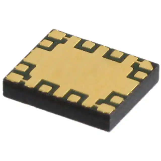
The ALM-31222 is housed inside a miniature 5.0 x 6.0 x 1.1
mm3 22-lead multiple-chips-on-board (MCOB) module
package.
Component Image
Top View
• Unconditionally stable across load condition
• Built-in adjustable temperature-compensated internal
bias circuitry
• GaAs E-pHEMT Technology[1]
• 5V supply
• Excellent uniformity in product specifications
• Tape-and-Reel packaging option available
• MSL-3 and Lead-free
• High MTTF for base station application
Specifications
2GHz; 5V, 415mA (typical)
• 14.9 dB Gain
• 47.9 dBm Output IP3
5.0 x 6.0 x 1.1 mm3 22-lead MCOB
20
21
22
• 52.6% PAE at P1dB
GND
19
GND
18
GND
VDD1
17
VCTRL
GND
GND
• 31.5 dBm Output Power at 1dB gain compression
1
RF_OUT
16
2
NC
GND
15
3
GND
GND
12
11
GND
10
9
8
7
6
GND
RF_IN
NC
GND
5
GND
4
GND
14
13
VDD2
GND
GND
GND
GND
GND
GND
31222
WWYY
XXXX
• High linearity and P1dB
Bottom View
Notes:
Package marking provides orientation and identification
“31222” = Device Part Number
“WWYY” = Work week and Year of manufacture
“XXXX” = Last 4 digit of Lot number
• 2.7 dB Noise Figure
Applications
• Class A driver amplifier for GSM/PCS/W-CDMA/WiMAX
Base Stations.
• General purpose gain block.
Note:
1. Enhancement mode technology employs positive gate voltage,
thereby eliminating the need of negative gate voltage associated
with conventional depletion mode devices.
Attention: Observe precautions for
handling electrostatic sensitive devices.
ESD Machine Model = 200 V
ESD Human Body Model = 500 V
Refer to Avago Application Note A004R:
Electrostatic Discharge, Damage and Control.
�Absolute Maximum Rating [2] TA=25°C
Symbol
Parameter
Units
Absolute Max.
Ids, max
Device Drain Current
mA
750
Vctrl,max
Control Voltage
V
5.5
Pin,max
CW RF Input Power
dBm
25
Pdiss
Total Power Dissipation [4]
W
4.125
Tj,max
Junction Temperature
oC
150
TSTG
Storage Temperature
oC
-65 to 150
Vdd, max
Device Voltage, RF output to ground
V
5.5
Thermal Resistance [3] θjc = 25 °C/W
(Vdd = 5V, Idd = 400mA, Tc = 85 °C)
Notes:
2. Operation of this device in excess of any of
these limits may cause permanent damage.
3. Thermal resistance measured using Infra-Red
measurement technique.
4. This is limited by maximum Vdd and Ids.
Derate 40mW/ °C for TC>46.9 °C.
Product Consistency Distribution Charts[5, 6]
CPK = 4.51
Std Dev = 0.254
CPK = 1.26
Std Dev = 10.6
.36
.38
.4
.42
.44
.46
.48
Figure 1: Ids; LSL = 370mA, nominal = 415mA, USL = 470mA
.5
CPK = 12.1
Std Dev = 0.042
30
30.5
31
31.5
Figure 3: P1dB; LSL = 30dBm, nominal = 31.5dBm
44.5
45 45.5
46 46.5
47 47.5
Figure 2: OIP3; LSL = 44.5dBm, nominal = 47.9dBm
48
48.5
49
Std Dev = 0.254
32
50
51
52
53
Figure 4: PAE at P1dB; nominal = 52.6%
54
55
CPK = 5.0
Std Dev = 0.085
13.5
14
14.5
15
15.5
16
16.5
Figure 5: Gain; LSL=13.7dB, Nominal = 14.9dB, USL=16.8dB
�
17
Notes:
5. Distribution data sample size is 500 samples taken from 2 different
wafers lots. TA = 25°C, Vdd = 5V, Vctrl = 5V, RF performance at 2GHz
unless otherwise specified. Future wafers allocated to this product
may have nominal values anywhere between the upper and lower
limits.
6. Measurements are made on a production test board. Input trace
losses have not been de-embedded from actual measurements.
�Electrical Specifications [7]
TA = 25 °C, Vdd =5V, Vctrl=5V, RF performance at 2.0 GHz, measured on demo board (see Figure 7) unless otherwise
specified.
Symbol
Parameter and Test Condition
Units
Min.
Typ.
Max.
Ids
Quiescent current
mA
370
415
470
Ictrl
Vctrl current
mA
-
10.4
-
Gain
Gain
dB
13.7
14.9
16.8
OIP3 [8]
Output Third Order Intercept Point
dBm
44.5
47.9
-
OP1dB
Output Power at 1dB Gain Compression
dBm
30
31.5
-
PAE
Power Added Efficiency
%
-
52
-
NF
Noise Figure
dB
-
2.7
-
S11
Input Return Loss, 50Ω source
dB
-
-10
-
S22
Output Return Loss, 50Ω load
dB
-
-10
-
S12
Reverse Isolation
dB
-
-30
-
Notes:
7. Measurements at 2GHz obtained using demo board described in Figure 6 and 7.
8. 2GHz OIP3 test condition: FRF1 - FRF2 = 10MHz with input power of -5dBm per tone measured at worse case side band.
9. Use proper bias, heat sink and de-rating to ensure maximum channel temperature is not exceeded. See absolute maximum ratings and
application note (if applicable) for more details.
�
�S-Parameter (Vdd=5V, Vctrl=5V, T=25°C, matched 50 ohm)
Freq (GHz)
S11 (dB)
S11 (ang)
S21 (dB)
S21 (ang)
S12 (dB)
S12 (ang)
S22 (dB)
S22 (ang)
0.1
-0.28
175.96
-83.18
176.23
-85.32
-67.51
-1.24
-142.79
0.2
-0.33
173.13
-52.64
161.11
-79.55
71.39
-1.1
-167.79
0.3
-0.32
169.83
-39.35
128.52
-75.05
83.66
-1.02
179.87
0.4
-0.38
166.32
-29.95
100.99
-69.64
85.21
-0.99
169.14
0.5
-0.39
162.45
-23.54
79.41
-68.48
69.93
-1.01
158.91
0.6
-0.51
158
-17.63
69.24
-65.17
52.89
-1.05
147.9
0.7
-0.57
152.77
-11.35
54.33
-60.41
26.3
-1.17
134.94
0.8
-0.78
146.84
-5.72
35.54
-56.11
6.3
-1.45
119.17
0.9
-0.82
139.57
-0.4
13.28
-51.07
-19.9
-2.03
99.51
1
-1.16
129.83
4.3
-13.32
-46.1
-49.33
-3.2
75.34
1.1
-1.48
119.45
8.01
-41.24
-42.01
-78.55
-5.01
50.04
1.2
-2.16
104.83
11.14
-73.66
-38.32
-111.37
-7.73
22.1
1.3
-3.45
86.86
13.49
-106.74
-35.37
-144.38
-10.47
-3.04
1.4
-5.75
64.05
15.1
-139.71
-33.12
-176.73
-11.98
-25.11
1.5
-9.86
34.92
16.01
-171.85
-31.64
151.79
-11.99
-48.46
1.6
-16.32
-12.66
16.29
157.85
-30.83
122.31
-11.45
-73.83
1.7
-18.73
-104.19
16.1
130.8
-30.55
96.01
-11.22
-98.63
1.8
-15.14
-151.56
15.8
108.62
-30.51
74.43
-11.43
-119.98
1.9
-12.68
-179.03
15.4
86.61
-30.55
52.91
-12.04
-141.78
2
-11.46
157.09
15.05
64.4
-30.61
31.14
-13.09
-165.11
2.1
-10.95
139.46
14.78
46.1
-30.69
13.01
-14.18
174.4
2.2
-10.67
120.01
14.51
26.44
-30.8
-6.7
-15.59
149.47
2.3
-10.67
101.25
14.25
6.6
-30.97
-26.97
-17.05
119.92
2.4
-10.76
80.58
13.98
-13.62
-31.23
-47.79
-18.2
83.09
2.5
-11.08
60.42
13.69
-32.78
-31.57
-67.87
-18.1
43.43
2.6
-11.15
35.78
13.32
-54.85
-32.11
-90.91
-16.32
1.98
2.7
-11.14
8.61
12.79
-78.85
-32.95
-114.76
-13.6
-31.62
2.8
-10.62
-17.4
11.76
-105.67
-34.13
-137.54
-10.54
-58.62
2.9
-9.29
-41.86
9.7
-131.03
-34.8
-158.21
-7.5
-85.47
3
-7.64
-67.59
7.59
-150.93
-35.42
175.41
-5.5
-111.51
3.1
-6.29
-92.79
5.59
-171.05
-36.65
148.66
-4.2
-132.99
3.2
-5.37
-113.14
3.48
170.73
-38.05
126.66
-3.34
-149.42
3.3
-4.44
-133.05
0.91
152.1
-39.61
105.49
-2.67
-164.34
3.4
-3.78
-150.27
-1.89
135.32
-41.07
87.89
-2.19
-176.6
3.5
-3.23
-165.06
-4.83
120.49
-42.43
73.22
-1.87
173.41
3.6
-2.89
-178.18
-7.85
107.48
-43.41
61.54
-1.65
165.31
3.7
-2.64
170.43
-10.94
96.02
-44.11
52.9
-1.5
158.68
3.8
-2.53
159.49
-14.05
85.79
-44.41
45.89
-1.38
153.37
3.9
-2.55
149.92
-17.01
77.16
-44.37
39.92
-1.3
149.34
4
-2.7
138.27
-20.45
68.04
-43.94
32.99
-1.23
145.77
�
�Freq (GHz)
S11 (dB)
S11 (ang)
S21 (dB)
S21 (ang)
S12 (dB)
S12 (ang)
S22 (dB)
S22 (ang)
4.1
-3.12
124.98
-24.48
59.64
-43.26
24.59
-1.19
142.81
4.2
-4
107.04
-29.94
54.26
-42.41
14.09
-1.16
140.48
4.3
-5.88
80.14
-38.62
78.06
-41.52
0.14
-1.14
138.59
4.4
-9.12
29.56
-35.16
141.21
-40.94
-18.9
-1.14
137.06
4.5
-8.89
-53.48
-31.02
131.79
-41.43
-41.31
-1.14
135.82
4.6
-5.46
-101.97
-30.5
114.9
-43
-59.92
-1.15
134.88
4.7
-3.25
-130.17
-31.67
99.57
-45.29
-73.84
-1.17
134.07
4.8
-2.22
-146.59
-33.51
88.44
-47.71
-82.07
-1.19
133.29
4.9
-1.67
-156.9
-35.58
80.35
-49.9
-85.77
-1.21
132.54
5
-1.38
-164.03
-37.74
74.33
-51.68
-87.52
-1.25
131.78
5.1
-1.19
-168.88
-39.92
69.9
-53.54
-88.6
-1.29
130.96
5.2
-1.08
-172.79
-42
66.23
-55.04
-88.69
-1.34
130.02
5.3
-1
-175.55
-44.09
63.38
-56.69
-88.55
-1.39
128.84
5.4
-0.97
-177.74
-46.1
60.82
-57.75
-86.81
-1.45
127.63
5.5
-0.93
-179.47
-48.16
58.9
-59.67
-84.83
-1.51
125.96
5.6
-0.91
178.98
-50.38
55.72
-61.1
-80.67
-1.6
123.94
5.7
-0.89
177.9
-52.39
55.19
-62.67
-75.2
-1.69
121.57
5.8
-0.88
176.77
-54.31
53.59
-64.48
-61.6
-1.78
118.67
5.9
-0.89
175.77
-56.07
50.42
-65.31
-47.79
-1.9
115.35
6
-0.91
174.44
-58.26
46.84
-64.83
-33.25
-2.01
111.39
�
�Demo Board Schematic
3
Vsense
Vsupply
8
Vctrl
1,2,19,20
R1
1,22
2
3,4
5
C3
21
C2
20 19
C1
C4
Z1
17,18
Bias
Input
match
50-Ohms TL
C5
16
Output
match
50-Ohms TL
6
12,13,14,15
7
8
9
10
Module Outline
C8
C7
C6
Size
Value
Description
C1, C6
0805
2.2uF
Ceramic Chip Capacitor
C2, C4, C8
0402
0.1uF
Ceramic Chip Capacitor
C3, C5, C7
0402
10nF
Ceramic Chip Capacitor
R1
0805
0 Ohm
Chip Resistor
R2
0805
Not Used
N/A
Z1, Z2
0805
Not Used
Zener Diode 5.6V
(Optional)
Z2
Vsupply
R2
11
Circuit Symbol
1,2,19,20
Figure 6. Demo board application schematics and components table
Demo Board Layout
Pins pointing out of the page
Unit is on top
20-pin Connector
10
1 2 3 4 5 6 7 8 9 10
1
20 19 18 17 16 15 14 13 12 11
Pins 1,2,19,20 = Vsupply = Vdd
Pin 3 = Vsense (optional)
Pins 5,6,15,16 = GND
Pin 8 = Vctrl
RF
input
Other pins are not used
Figure 7. Demo Board Layout Diagram
1. Recommended PCB material is 10 mils Rogers RO4350, with FR4 backing for mechanical strength.
2. Suggested component values may vary according to layout and PCB material.
�
RF
output
�ALM-31222 Typical Performance
TA = +25°C, Vdd = 5V, Vctrl = 5V, Input Signal=CW unless stated otherwise.
500
480
440
OIP3 (dB)
Ids (mA)
460
420
400
380
360
340
-40 -30 -20 -10 0
10 20 30 40 50 60 70 80 90
Temperature (ºC)
34
18
33
17
32
16
31
30
29
85ºC
25ºC
-40ºC
28
27
1.7
1.8
1.9
2
1.9
2
2.1 2.2 2.3
Frequency (GHz)
2.4
2.5
2.6
2.7
2.4
2.5
2.6
2.7
2.1 2.2 2.3 2.4
Frequency (GHz)
2.5
2.6
2.7
15
14
13
85ºC
25ºC
-40ºC
2.1 2.2 2.3
Frequency (GHz)
2.4
2.5
2.6
10
2.7
1.7
1.8
1.9
2
2.1 2.2 2.3
Frequency (GHz)
Figure 11. Over temperature Gain vs Frequency
0
85ºC
25ºC
-40ºC
-5
-5
-10
S22 (dB)
S11 (dB)
1.8
11
0
-15
-20
-10
-15
85ºC
25ºC
-40ºC
-20
1.8
1.9
2
2.1 2.2 2.3
Frequency (GHz)
Figure 12. Over temperature S11 vs Frequency
�
1.7
12
Figure 10. Over temperature P1dB vs Frequency
-25
1.7
85ºC
25ºC
-40ºC
Figure 9. Over temperature OIP3 vs Frequency
Gain (dB)
P1dB (dBm)
Figure 8. Ids vs Temperature
50
49
48
47
46
45
44
43
42
41
40
2.4
2.5
2.6
2.7
-25
1.7
1.8
1.9
2
Figure 13. Over temperature S22 vs Frequency
�ALM-31222 Typical Performance
-25
-26
-27
-28
-29
-30
-31
-32
-33
-34
-35
85ºC
25ºC
-40ºC
EVM(%)
S12 (dB)
TA = +25°C, Vdd = 5V, Vctrl = 5V, Input Signal=CW unless stated otherwise.
1.7
1.8
1.9
2
2.1 2.2 2.3
Frequency (GHz)
2.4
2.5
2.6
2.7
Figure 14. Over temperature S12 vs Frequency
85ºC
25ºC
-40ºC
-30
-35
-30
-40
-45
19
20
21
Pout(dBm)
22
23
24
25
-45
-55
-55
20
21
22
23
Output Channel Power (dBm)
24
-60
25
3GPP WCDMA
Test Model 1 +64DPCH
+/- 5MHz Offset
-40
-50
20
21
22
23
Output Channel Power (dBm)
24
25
Figure 17. Over temperature ACPR vs Channel Power at 2.5GHz
Figure 16. Over temperature ACPR vs Channel Power at 2.14GHz
-20
-20
-25
85ºC
25ºC
-40ºC
-30
-25
3GPP WCDMA
Test Model 1 +64DPCH
+/- 5MHz Offset
-40
-45
-35
-45
-50
-55
-55
21
22
23
Output Channel Power (dBm)
24
Figure 18. Over temperature ACPR vs Channel Power at 2.6GHz
25
3GPP WCDMA
Test Model 1 +64DPCH
+/- 5MHz Offset
-40
-50
20
85ºC
25ºC
-40ºC
-30
ACPR (dBC)
-35
-60
18
-35
-50
-60
17
85ºC
25ºC
-40ºC
-25
3GPP WCDMA
Test Model 1 +64DPCH
+/- 5MHz Offset
ACPR (dBC)
ACPR (dBC)
16
IEEE 802.16d
64-QAM
BW20MHz
-20
-25
ACPR (dBC)
85ºC
25ºC
-40ºC
Figure 15. Over temperature EVM vs Pout at 2.5GHz
-20
�
5.0
4.5
4.0
3.5
3.0
2.5
2.0
1.5
1.0
0.5
0.0
-60
20
21
22
23
Output Channel Power (dBm)
24
Figure 19. Over temperature ACPR vs Channel Power at 2.7GHz
25
�PCB Layout and Stencil Design
5.80
0.50
Pin 1
0.50
0.41
5.73
0.35
0.35
0.54
0.45
0.41
0.35
0.50
2.79
4.80
4.20
0.45
1.74
0.39
1.30
0.77
1.17
0.30
0.72
0.30
0.85
0.45
0.60
0.70
0.30
0.30
0.45
0.35
0.63
Stencil Opening
PCB Land Pattern
5.80
5.73
4.74 4.80
Combines Land Pattern and Stencil Layout
Note:
All dimensions are in millimeters.
�
0.45
0.45
4.74
�MCOB 5x6 Package Dimensions
0.60 (PCB Thickness)
6.00±0.10
Pin 1
31222
WWYY
XXXX
5.00±0.10
1.05±0.10
Side View
Top View
(8x) 0.21
0.07 (All Metal and SM Gaps)
19
18
17
21
20
22
(8x) 0.210
(12x) 0.16
(8x) 0.50 sq
1
16
2
15
3
14
4
13
5
12
11
10
9
8
7
6
(2x) 1.30
(2x) 2.40
(4x) 0.60
0.10
(6x) 0.50
(2x) 1.60
(4x) 0.70
Bottom View
Part Number Ordering Information
Product Family
Part Number
No. of Devices
Container
ALM31222-TR1G
1000
Frequency Band
7” Reel
Output
Power
700MHz-1GHz
1.7- 2.7GHz
3.3-3.9GHz
0.5W
MGA-30116
MGA-30216
MGA-30316
1W
ALM-31122
ALM-31222
ALM-31322
2W
ALM-32120
ALM-32220
ALM-32320
ALM31222-TR2G
3000
13” Reel
ALM31222-BLKG
100
antistatic bag
10
Notes:
1. All dimenions are in milimeters
2. Dimensions are inclusive of plating
3. Dimensions are exclusive of mold flash and metal burr
�Device Orientation
REEL
USER FEED DIRECTION
31222
WWYY
XXXX
31222
WWYY
XXXX
CARRIER
TAPE
31222
WWYY
XXXX
TOP VIEW
USER
FEED
DIRECTION
END VIEW
COVER TAPE
Tape Dimensions
4.00±0.10 See Note #2
Section B-B
(R0.50)
A
B
8.00±0.10
0.30±0.05
Ko
Ao
11
Section A-A
Ø1.50 (Min)
12.00±0.30
Bo
1.75±0.10
5˚ All
Around
A
5.50±0.10
Ø1.55±0.05
2.00±0.05
B
�Reel Dimension - 7 inch
6.25mm EMBOSSED LETTERS
LETTERING THICKNESS: 1.6mm
SLOT HOLE "a"
SEE DETAIL "X"
Ø178.0±0.5
SLOT HOLE "b"
FRONT
BACK
6
PS
SLOT HOLE(2x)
180° APART.
SLOT HOLE "a": 3.0±0.5mm(1x)
SLOT HOLE "b": 2.5±0.5mm(1x)
FRONT VIEW
1.5 MIN.
+1.5*
-0.0
+0.5
Ø13.0 -0.2
Ø20.2 MIN.
45°
EMBOSSED RIBS
RAISED: 0.25mm, WIDTH: 1.25mm
BACK VIEW
12
BACK
Ø55.0±0.5
FRONT
Ø178.0±0.5
Ø51.2±0.3
SEE DETAIL "Y"
18.0*
MAX.
DETAIL "X"
Ø178.0±0.5
R5.2
°
R10.65
120
65°
12.4
45°
3.5
DETAIL "Y"
(Slot Hole)
1.0
6
PS
RECYCLE LOGO
�Reel Dimension - 13 inch
11
12 1
2
3
4
0 2
10
9
7
6
5
DATE CODE
12MM
8
EMBOSSED LETTERING
16.0mm HEIGHT x MIN. 0.4mm THICK.
Ø329.0±1.0
HUB
Ø100.0±0.5
6
PS
02
12
12
10
911
876534
MP
N
CPN
EMBOSSED LETTERING
7.5mm HEIGHT
EMBOSSED LETTERING
7.5mm HEIGHT
1.5
(MI
N.)
FRONT VIEW
EMBOSSED LINE (2x)
89.0mm LENGTH LINES 147.0mm
AWAY FROM CENTER POINT
+0.5
-0.2
20.2(MIN.)
Ø13.0
11.9-15.4**
+2.0*
12.4
-0.0
Ø16.0
ESD LOGO
6
PS
RECYCLE LOGO
Detail "X"
SEE DETAIL "X"
Ø100.0±0.5
Ø329.0±1.0
6
PS
R19.0±0.5
BACK VIEW
SLOT
5.0±0.5(3x)
Ø12.3±0.5(3x)
For product information and a complete list of distributors, please go to our web site:
18.4 MAX.*
www.avagotech.com
Avago, Avago Technologies, and the A logo are trademarks of Avago Technologies Limited in the United States and other countries.
Data subject to change. Copyright © 2005-2008 Avago Technologies Limited. All rights reserved.
AV02-1179EN - May 13, 2008
�