ALMD-EL3D, ALMD-EG3D, ALMD-CM3D, ALMD-CB3D
High Brightness SMT Round LED Lamps
Amber, Red, Green and Blue Tinted LEDs
Data Sheet
Description
Features
The new Avago ALMD-xx3D LED series has the same or
just slightly less luminous intensity than conventional
high brightness, through-hole LEDs.
• Compact form factor
The new LED lamps can be assembled using common
SMT assembly processes and are compatible with industrial reflow soldering processes.
• High brightness material
• Available in Red, Amber, Green and Blue color
• Red AlInGaP 626 nm
• Amber AlInGaP 590 nm
The LEDs are made with an advanced optical grade epoxy
for superior performance in outdoor sign applications.
• Green InGaN 525 nm
For easy pick and place assembly, the LEDs are shipped
in EIA-compliant tape and reel. Every reel is shipped from
a single intensity and color bin– except the red color–for
better uniformity.
• JEDEC MSL 2A
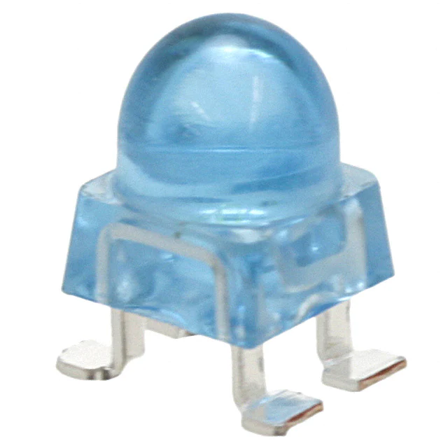
Package Dimensions
• Blue InGaN 470 nm
• Compatible with industrial reflow soldering process
• Typical Viewing angle: 30°
• Tinted, non-diffused
Applications
Package Marking
• Variable Message Signs
A
A
4.20 ± 0.20
C
C
A: Anode
C: Cathode
4.20 ± 0.20
4.75 ± 0.50
6.50 ± 0.50
3.40 ± 0.50
2.50 ± 0.20
C
A
1.4 (4x)
Notes:
1. All dimensions in millimeters (inches).
2. Tolerance is ± 0.20 mm unless other specified.
3. Copper leadframe.
CAUTION: InGaN devices are Class 1C HBM ESD sensitive, AlInGaP devices are Class 1B ESD sensitive per JEDEC Standard.
Please observe appropriate precautions during handling and processing. Refer to Application Note AN-1142 for additional details.
CAUTION: Customer is advised to keep the LED in the MBB when not in use as prolonged exposure to environment might cause
the silver plated leads to tarnish, which might cause difficulties in soldering.
�Device Selection Guide
Part Number
Color and Dominant Wavelength
λd (nm) Typ [3]
Luminous Intensity Iv (mcd) [1,2,5]
Min
Max
Viewing Angle
Typ (°) [4]
ALMD-EG3D-VX002
Red 626
4200
9300
30°
ALMD-EL3D-VX002
Amber 590
4200
9300
ALMD-CM3D-Y1002
Green 525
9300
21000
ALMD-CB3D-SU002
Blue 470
1900
4200
Notes:
1. The luminous intensity is measured on the mechanical axis of the lamp package and it is tested with pulsing condition.
2. The optical axis is closely aligned with the package mechanical axis.
3. Dominant wavelength, λd, is derived from the CIE Chromaticity Diagram and represents the color of the lamp.
4. θ½ is the off-axis angle where the luminous intensity is half the on-axis intensity.
5. Tolerance for each bin limit is ± 15%
Part Numbering System
A
L
M
D
-
x1
x2
x3
x4
-
x5
x6
x7
x8
x9
Code
Description
Option
x1
Package type
E
C
Round AlInGaP
Round InGaN
x2
Color
B
G
L
M
Blue
Red
Amber
Green
x3
Viewing angle
3
30°
x4
Product specific designation
D
x5
Minimum intensity bin
Refer to device selection guide
x6
Maximum intensity bin
Refer to device selection guide
x7
Color bin selection
0
Full distribution
x8x9
Packaging option
02
Tested 20mA, 13inch carrier tape
2
�Absolute Maximum Rating, TJ = 25 °C
Parameter
Red and Amber
Blue and Green
Unit
50
30
mA
100 [2]
100 [3]
mA
114
mW
DC Forward Current [1]
Peak Forward Current
120
Power Dissipation
Reverse Voltage
5 (IR
= 100 μA) [4]
5 (IR
= 10 μA) [4]
V
110
°C
Operating Temperature Range
-40 to +85
°C
Storage Temperature Range
-40 to +100
°C
LED Junction Temperature
Notes:
1. Derate linearly as shown in Figure 4 and Figure 9.
2. Duty Factor 30%, frequency 1 kHz.
3. Duty Factor 10%, frequency 1 kHz.
4. Indicates product final testing; long-term reverse bias is not recommended.
Electrical / Optical Characteristics, TJ = 25 °C
Parameter
Symbol
Forward Voltage
Red
Amber
Green
Blue
VF
Reverse Voltage
Red & Amber
Green & Blue
VR
Dominant Wavelength [1]
Red
Amber
Green
Blue
λd
Peak Wavelength
Red
Amber
Green
Blue
Thermal Resistance
Luminous Efficacy [2]
Red
Amber
Green
Blue
Thermal coefficient of λd
Red
Amber
Green
Blue
Min.
1.8
1.8
2.8
2.8
Typ.
2.1
2.1
3.2
3.2
Max.
2.4
2.4
3.8
3.8
5
5
618.0
584.5
519.0
460.0
626.0
590.0
525.0
470.0
Units
Test Conditions
V
IF = 20 mA
V
IF = 100 µA
IF = 10 µA
IF = 20 mA
630.0
594.5
539.0
480.0
λPEAK
634
594
516
464
nm
Peak of Wavelength of Spectral
Distribution at IF = 20 mA
RθJ-PIN
130
°C/W
LED Junction-to-Pin
ηV
200
520
530
65
lm/W
Emitted Luminous Power/Emitted
Radiant Power
nm/°C
IF = 20 mA ; +25 °C ≤ TJ ≤ +100 °C
0.059
0.103
0.028
0.024
Notes:
1. The dominant wavelength is derived from the chromaticity diagram and represents the color of the lamp.
2. The radiant intensity, Ie in watts per steradian, may be found from the equation Ie = IV/ηV where IV is the luminous intensity in candelas and ηV is
the luminous efficacy in lumens/watt.
3
�AlInGaP
100
RELATIVE INTENSITY
0.8
Amber
FORWARD CURRENT - mA
1
Red
0.6
0.4
0.2
0
500
550
600
WAVELENGTH - nm
40
20
0
0.5
1
1.5
2
FORWARD VOLTAGE - V
2.5
60
Amber
Red
0
20
40
60
FORWARD CURRENT - mA
80
100
50
40
30
20
10
0
0
20
40
60
TA - AMBIENT TEMPERATURE (°C)
80
Note: RθJ-A = 460 °C/W
RELATIVE DOMINANT WAVELENGTH
SHIFT(NORMALIZED AT 20mA) - nm
Figure 3. Relative Intensity vs Forward Current
1.6
1.4
1.2
1.0
0.8
0.6
0.4
0.2
0.0
-0.2
-0.4
-0.6
Figure 4. Maximum Forward Current vs Ambient Temperature
Amber
Red
0
20
40
60
FORWARD CURRENT - mA
80
Figure 5. Relative Dominant Wavelength Shift vs Forward Current
4
3
Figure 2. Forward Current vs Forward Voltage
MAXIMUM FORWARD CURRENT - mA
RELATIVE LUMINOUS INTENSITY
(NORMALIZED AT 20mA)
60
0
650
Figure 1. Relative Intensity vs Wavelength
5.0
4.5
4.0
3.5
3.0
2.5
2.0
1.5
1.0
0.5
0.0
80
100
100
�1.0
0.9
0.8
0.7
0.6
0.5
0.4
0.3
0.2
0.1
0.0
100
BLUE
FORWARD CURRENT-mA
RELATIVE INTENSITY
InGaN
GREEN
380
430
480
530
WAVELENGTH - nm
580
630
Figure 6. Relative Intensity vs Wavelength
0
IFmax - MAXIMUM FORWARD
CURRENT - mA
RELATIVE LUMINOUS INTENSITY
(NORMALIZED AT 20mA)
2.5
Green
2.0
1.5
1.0
0.5
0
20
40
60
80
DC FORWARD CURRENT-mA
100
120
0
1
2
3
FORWARD VOLTAGE-V
4
5
40
60
80
TA - AMBIENT TEMPERATURE - °C
100
5
Green
Blue
0
-5
0
20
30
25
20
15
10
5
0
0
20
Figure 9. Maximum Forward Current vs Ambient Temperature
10
RELATIVE DOMINANT
WAVELENGTH SHIFT -nm
20
Figure 7. Forward Current vs Forward Voltage
Figure 8. Relative Intensity vs Forward Current
40
60
FORWARD CURRENT-mA
Figure 10. Dominant Wavelength Shift vs Forward Current
5
40
Blue
3.0
-10
60
35
3.5
0.0
80
80
100
�NORMALIZED INTENSITY
1.0
0.8
0.6
Package Marking
0.4
A
X
0.2
0.0
-90
-60
-30
0
30
ANGULAR DISPLACEMENT-DEGREE
60
Figure 11b. Component Axis for Radiation Pattern
0.3
Red
Amber
Blue
Green
FORWARD VOLTAGE SHIFT-V
NORMALZIED INTENSITY (PHOTO)
C
90
10
1
-40
-15
10
35
TJ - JUNCTION TEMPERATURE
60
85
0.7
4.0
Figure 12. Relative Intensity Shift vs Junction Temperature
2.1
5.2
Note: Recommended stencil thickness is 0.1524mm (6 mils) minimum
and above.
Figure 14. Recommended Soldering Land Pattern
6
X
C
Figure 11a. Radiation Pattern for X axis
0.1
A
Red
Amber
0.2
Green
Blue
0.1
0
-0.1
-0.2
-0.3
-40
-15
10
35
TJ - JUNCTION TEMPERATURE
Figure 13. Forward Voltage Shift vs Junction Temperature
60
85
�0.50±0.10
4.00±0.20 2.00±0.20
1.55±0.20
1.75±0.20
1.80±0.20
7.50±0.20
5.20±0.20
2.20±0.20
4.50±0.20
8.00±0.20
16.00±0.30
1.60±0.20
5.30±0.20 7.10±0.20
Figure 15. Carrier Tape Dimension
∅100 ± 0.50
16.40 ± 0.20
∅330 MAX.
13.00 ± 0.20
Figure 16. Reel Dimension
2 anode leads lead unreeling direction
Figure 17. Unit Orientation from reel
7
�Intensity Bin Limit Table (1.3:1 Iv bin ratio)
VF Bin Table (V at 20 mA) for Red & Amber
Intensity (mcd) at 20 mA
Bin
Min
Max
S
1900
2500
T
2500
3200
U
3200
4200
V
4200
5500
W
5500
7200
X
7200
9300
Y
9300
12000
Z
12000
16000
1
16000
21000
Bin ID
Min
Max
VD
1.8
2.0
VA
2.0
2.2
VB
2.2
2.4
Tolerance for each bin limit is ± 0.05V
Tolerance for each bin limit is ± 15%
Red Color Range
Green Color Range
Min Dom
Max Dom X min
Y Min
X max
Y max
0.2943
Min
Bin Dom
Max
Dom
618.0
630.0
0.6872
0.3126
0.6890
Xmin
Ymin
Xmax
Ymax
0.6690
0.3149
0.7080
0.2920
1
519.0
523.0
0.0667
0.8323
0.1450
0.7319
0.1200
0.7375
0.0979
0.8316
2
523.0
527.0
0.0979
0.8316
0.1711
0.7218
0.1450
0.7319
0.1305
0.8189
0.1305
0.8189
0.1967
0.7077
0.1711
0.7218
0.1625
0.8012
0.1625
0.8012
0.2210
0.6920
0.1967
0.7077
0.1929
0.7816
0.1929
0.7816
0.2445
0.6747
0.2210
0.6920
0.2233
0.7600
Tolerance for each bin limit is ± 0.5nm
Amber Color Range
Bin
Min
Dom
Max
Dom
Xmin
Ymin
Xmax
Ymax
1
584.5
587.0
0.5420
0.4580
0.5530
0.4400
0.5370
0.4550
0.5570
0.4420
0.5570
0.4420
0.5670
0.4250
0.5530
0.4400
0.5720
0.4270
0.5720
0.4270
0.5820
0.4110
0.5670
0.4250
0.5870
0.4130
0.5870
0.4130
0.5950
0.3980
0.5820
0.4110
0.6000
0.3990
2
4
6
587.0
589.5
592.0
589.5
592.0
594.5
Tolerance for each bin limit is ± 0.5nm
3
527.0
531.0
4
531.0
535.0
5
535.0
539.0
Tolerance for each bin limit is ± 0.5nm
Blue Color Range
Min
Bin Dom
Max
Dom
Xmin
Ymin
Xmax
Ymax
1
464.0
0.1440
0.0297
0.1766
0.0966
0.1818
0.0904
0.1374
0.0374
0.1374
0.0374
0.1699
0.1062
0.1766
0.0966
0.1291
0.0495
0.1291
0.0495
0.1616
0.1209
0.1699
0.1062
0.1187
0.0671
0.1187
0.0671
0.1517
0.1423
0.1616
0.1209
0.1063
0.0945
0.1063
0.0945
0.1397
0.1728
0.1517
0.1423
0.0913
0.1327
2
460.0
464.0
468.0
3
468.0
472.0
4
472.0
476.0
5
476.0
480.0
Tolerance for each bin limit is ± 0.5nm
8
�Packing Label
(i) Mother Label (Available on MBB bag)
(1T) Lot: Lot Number
STANDARD LABEL LS0002
RoHS Compliant
(Q) QTY: Quantity
e4 Max Temp 260C MSL 2a
LPN:
CAT: Intensity Bin
(9D)MFG Date: Manufacturing Date
BIN: Refer to below information
(1P) Item: Part Number
(P) Customer Item:
(V) Vendor ID:
(9D) Date Code: Date Code
DeptID: OEAT01
Made In: Country of Origin
(ii) Baby Label (Available on Plastic Reel)
(1P) PART #: Part Number
(1T) Lot #: Lot Number
(9D)MFG Date: Manufacturing Date
C/0: Country of Origin
(1T) TAPE DATE: Taping Date
BABY LABEL COSBOO1B V0.0
(Q) QTY: Quantity
(9D) Date Code: Date Code
CAT Intensity Bin
BIN Refer to Below information
Note: Acronyms and Definition:
Example:
BIN:
a. Color bin only or VF bin only
(i) Color bin only or VF bin only
BIN: 4 (represent color bin 4 only)
(Applicable for part number with color bins but without VF bin OR part number with VF bins and no color
bin)
(ii) Color bin incorporated with VF bin
Applicable for part number that have both color bin
and VF bin
BIN: VA (represent VF bin “VA” only)
b. Color bin incorporate with VF bin
BIN: 4 VA
VA: VF bin “VA”
4: Color bin 4 only
9
�Soldering
Recommended reflow soldering condition:
(i) Leaded reflow soldering:
(ii) Lead-free reflow soldering:
20 SEC. MAX.
183°C
100-150°C
-6°C/SEC.
MAX.
3°C/SEC.
MAX.
120 SEC. MAX.
60-150 SEC.
TIME
a. Reflow soldering must not be done more than two
times. Make sure you take the necessary precautions
for handling a moisture-sensitive device, as stated in
the following section.
b. Recommended board reflow direction:
TEMPERATURE
TEMPERATURE
10 to 30 SEC.
240°C MAX.
3°C/SEC. MAX.
217°C
200°C
255 - 260 °C
3°C/SEC. MAX.
6°C/SEC. MAX.
150°C
3 °C/SEC. MAX.
100 SEC. MAX.
60 - 120 SEC.
TIME
c. Do not apply any pressure or force on the LED during
reflow and after reflow when the LED is still hot.
d. It is preferred that you use reflow soldering to
solder the LED. Use hand soldering only for rework
if unavoidable but must be strictly controlled to the
following conditions:
- Soldering iron tip temperature = 320 °C max.
- Soldering duration = 3 sec max.
- Number of cycles = 1 only
- Power of soldering iron = 50 W max.
e. Do not touch the LED body with a hot soldering iron
except the soldering terminals as this may damage the
LED.
f. For de-soldering, it is recommended that you use a
double flat tip.
REFLOW SOLDERING
10
g. Please confirm beforehand whether the functionality
and performance of the LED is affected by hand
soldering.
�PRECAUTIONARY NOTES
d. Control of assembled boards
1. Handling precautions
For automated pick and place, Avago has tested nozzle
size below made with urethane material to be working
fine with this LED. However, due to the possibility of
variations in other parameters such as pick and place
machine maker/model and other settings of the machine, customer is recommended to verify the nozzle
selected.
- If the PCB soldered with the LEDs is to be
subjected to other high temperature processes,
the PCB need to be stored in sealed MBB with
desiccant or desiccator at 3.5mm
- The LEDs are exposed to condition of >30°C /
60% RH at any time.
- The LED floor life exceeded 672hrs.
LED flange
4.4 mm
∅3.9 mm
The recommended baking condition is: 60±5ºC
for 20hrs. Baking should only be done once.
f. Storage
Note:
a. Nozzle tip should touch the LED flange during pick and place.
b. Outer dimensions of the nozzle should be able to fit into the carrier
tape pocket.
2. Handling of moisture-sensitive device
This product has a Moisture Sensitive Level 2a rating
per JEDEC J-STD-020. Refer to Avago Application Note
AN5305, Handling of Moisture Sensitive Surface Mount
Devices, for additional details and a review of proper
handling procedures.
a. Before use
- An unopened moisture barrier bag (MBB) can
be stored at
很抱歉,暂时无法提供与“ALMD-CB3D-SU002”相匹配的价格&库存,您可以联系我们找货
免费人工找货- 国内价格 香港价格
- 1+14.741071+1.89084
- 10+10.4607210+1.34180
- 100+7.89891100+1.01320
- 500+6.76439500+0.86767
- 国内价格 香港价格
- 1000+6.393721000+0.82013
- 2000+6.079512000+0.77982
- 3000+5.918533000+0.75917
- 5000+5.736795000+0.73586
- 7000+5.628767000+0.72200
- 10000+5.5234310000+0.70849