APDS-9500
Imaging-Based Proximity and Gesture Sensor
Data Sheet
Description
Features
The APDS-9500 provides an imaging-based gesture
recognition function with an I2C-bus interface in a single
18-pin package. It can recognize nine gestures, including move up, move down, move left, move right, move
forward, move backward, circle-clockwise, circle-counterclockwise and wave. This gesture information can be
easily accessed via the I2C bus.
• Imaging-based proximity and gesture sensor in an
optical module
The APDS-9500 also provides built-in proximity detection
for sensing objects approaching or departing.
Applications
• Gesture Detection
• Cell Phone Touch-Screen Disable
• Mechanical Switch Replacement
Ordering Information
Part Number
Packaging
Quantity
APDS-9500
Tape and Reel
2500 per reel
• Gesture output
– Nine-gesture recognition
• Proximity output
– Object brightness output
– Object size output
• Cursor mode output
– X and Y output
• Image output
– SPI output
– 30 × 30 pixels/60 × 60 pixels
– 9-bit gray scale
• Ambient light immunity
• I2C-bus interface compatible
– Data rates up to 400 kHz
– Dedicated Interrupt pin
• Flexible power saving mode
• VDD range from 2.8V to 3.3V
• I/O voltage range from 1.8V to 3.3V
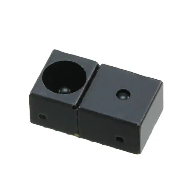
• Small package: 6.87 × 3.76 × 2.86 mm (L × W × H)
�Functional Block Diagram
VDD
VIO
GND
Sensor
Array
Power
Block
9-bit
A/D
Pre Processing
Frame Buffer
(Frame subtraction)
30x30
SPI
Master
SPI_MCLK
SPI_CSn
SPI_CLK
SPI_DATA
60x60
LED Driver
I2C
Reg. Bank
Timing Gen.
Interrupt
IR LED
Object
Extraction
Gesture
Recognition
I/O Pins Configuration
Pin
Name
1
NC
2
INT
3
GND
4
SPI_DATA
O
SPI data
5
SPI_CLK
O
SPI clock
6
NC
No connect
7
LDR_2
LED Drive 2
8
LED-K_1
LED Cathode
9
LED-A
LED anode, connect to VLED on PCB
10
VDDA_I/O
Connect to GND through decoupling capacitor
11
VDDAY_I/O
Connect to GND through decoupling capacitor
12
VDDA18_I/O
Connect to GND through decoupling capacitor
13
VDD
Power supply voltage
14
VIO
15
SPI_MCLK
I
SPI master clock
16
SPI_CSn
O
SPI chip select
17
I2C_SDA
I/O
I2C-bus serial data I/O terminal—serial data I/O for I2C-bus
18
I2C_SCL
I
I2C-bus serial clock input terminal—clock signal for I2C-bus serial data
2
Type
Description
No connect
O
Interrupt
Power supply ground
Power supply voltage
I2C_SDA
I2C_SCL
INT
�Absolute Maximum Ratings (unless otherwise specified, Ta = 25°C)
Parameter
Symbol
Supply voltage
LED supply voltage
LED pulse current [1]
Max.
Unit
VDD
4.0
V
VLED
4.6
V
ILED
2
A
I2C-bus pin, Int pin voltage
VBUS
I2C-bus pin, Int pin current
IBUS
Min.
–0.3
VDD + 0.3
V
10
mA
Max.
Unit
Recommended Operating Conditions (unless otherwise specified, Ta = 25°C)
Parameter
Symbol
Min.
Typ.
Operating temperature
TA
–20
+70
°C
Operating supply voltage
VDD
2.8
3.6
V
LED supply voltage
VLED
3.0
4.2
V
Peak LED pulse current [1]
ILED
I2C-bus pin, INT pin voltage
VBUS
I2C-bus pin, INT pin current
IBUS
720
1.8
860
mA
3.3
V
5
mA
Note:
1. Pulse width < 500 μs, duty cycle < 5%
Operating Characteristics (unless otherwise specified, Ta = 25°C, VDD = 2.8V)
Parameter
Symbol
Unit
Test Conditions
Suspend current
IDD_SUS
Min.
15
Typ.
Max.
μA
See Figure 13
Standby state 1 current
IDD_ST1
0.57
mA
See Figure 11
Standby state 2 current
IDD_ST2
0.37
mA
See Figure 12
Current consumption
for proximity detection
0.2
mA
1.
2.
3.
4.
Register R_AE_Exposure_UB, 0x48 = 0x10
Register R_AE_Exposure_UB, 0x49 = 0x00
Register R_IDLE_TIME, 0x65 = 0xCE
Register R_IDLE_TIME, 0x66 = 0x0B
Current consumption for
gesture detection
1
mA
1.
2.
3.
4.
Register R_AE_Exposure_UB, 0x48 = 0x48
Register R_AE_Exposure_UB, 0x49 = 0x00
Register R_IDLE_TIME, 0x65 = 0x96
Register R_IDLE_TIME, 0x66 = 0x00
I2C-bus input high voltage
VIH
0.7 × VBUS
VBUS + 0.3
V
I2C-bus input low voltage
VIL
–0.3
0.3 × VBUS
V
INT, I2C_SDA output low
voltage
VOL
0.1 × VBUS
V
3
�Proximity Characteristics (unless otherwise specified, Ta = 25°C, VDD = 2.8V)
Parameter
Min. Typ. Max.
PS ADC Count Value (No Object)
PS ADC Count Value (100 mm
Distance Object)
47
Unit
Test Conditions
0
5
counts
1. Dedicated duo power supply, VDD = 2.8V and VLED = 3V
2. R_LensShadingComp_EnH Register, 0x25 = 0x14
3. R_LED1_DAC_UB Register, 0x32 = 0x14
4. R_AE_Exposure_UB Register, 0x48 = 0x10
5. R_AE_Exposure_UB Register, 0x49 = 0x00
6. Open view (no glass) and no reflective object above the
module.
56
65
counts
1. Dedicated duo power supply, VDD = 2.8V and VLED = 3V
2. Reflecting object – 73 mm × 83 mm Kodak 90% grey card,
100 mm distance
3. R_LensShadingComp_EnH Register, 0x25 = 0x14
4. R_LED1_DAC_UB Register, 0x32 = 0x14
5. R_AE_Exposure_UB Register, 0x48 = 0x10
6. R_AE_Exposure_UB Register, 0x49 = 0x00
7. Open view (no glass) above the module.
AC Electrical Characteristics, VDD = 3 V, TA = 25°C (unless otherwise noted) *
Parameter
Symbol
Min.
Max.
Unit
Clock frequency (I2C-bus only)
fSCL
10
400
kHz
Bus free time between a STOP and START condition
tBUF
1.3
–
μs
Hold time (repeated) START condition. After this period, the first clock pulse
is generated
tHDSTA
0.6
–
μs
Set-up time for a repeated START condition
tSU;STA
0.6
–
μs
Set-up time for STOP condition
tSU;STO
0.6
–
μs
Data hold time
tHD;DAT
0
–
ns
Data set-up time
tSU;DAT
100
–
ns
LOW period of the SCL clock
tLOW
1.3
–
μs
HIGH period of the SCL clock
tHIGH
0.6
–
μs
tf
–
300
ns
Clock/data rise time
tr
–
300
ns
Input pin capacitance
Ci
–
10
pF
Clock/data fall time
* Specified by design and characterization; not production tested.
t LOW
tr
V IH
V IL
SCL
t HD;STA
t HD;DAT
t BUF
t HIGH
t SU;STA
t SU;STO
tSU;DAT
V IH
V IL
SDA
P
Stop
Condition
S
Start
Condition
Figure 1. Timing Diagrams
4
tf
S
P
�5
1.4
4.5
1.3
4
1.2
3.5
Normalized IDD at 3V
Normalized IDD at 25°C
1.5
1.1
1
0.9
3
2.5
2
0.8
1.5
0.7
1
0.6
2.6
2.7
2.8
2.9
3
3.1
3.2
3.3
3.4
3.5
3.6
3.7
0.5
–60
3.8
–40
–20
0
VDD (V)
20
40
60
80
100
Temperature (°C)
Figure 2. Normalized IDD (Suspend) vs. VDD.
Figure 3. Normalized IDD (Suspend) vs. Temperature.
1.5
1.4
1.4
1.3
1.3
1.2
Normalized IDD at 2.8V
Normalized IDD at 2.8V
1.2
1.1
1
0.9
1.1
1
0.8
0.9
0.7
0.6
–60
–40
–20
0
20
40
60
80
0.8
–60
100
–40
–20
0
Figure 4. Normalized IDD (Standby1) vs. Temperature.
60
80
100
1.1
1
1
0.9
0.9
0.8
0.8
0.7
Normalized Responsitivity
Normalized Responsitivity
40
Figure 5. Normalized IDD (Standby2) vs. Temperature.
1.1
0.6
0.5
0.4
0.3
0.7
0.6
0.5
0.4
0.3
0.2
0.2
0.1
0.1
0
0
100
200
300
400
500
600
700
800
Angle (°)
Figure 6. Normalized LED Spectral Radiant Intensity.
5
20
Temperature (°C)
VDD (V)
900 1000 1100 1200
0
–60
–40
–20
0
Angle (°)
Figure 7. Normalized LED Angular Emitting Profile.
20
40
60
�I2C-Bus Protocol
The I2C-bus standard provides for three types of bus
transactions: read, write, and a combined protocol.
During a write operation, the first byte written is a
command byte followed by data. In a combined protocol,
the first byte written is the command byte followed by
reading a series of bytes. If a read command is issued,
the register address from the previous command is used
for data access. Likewise, if the MSB of the command is
not set, the device writes a series of bytes at the address
stored in the last valid command with a register address.
The command byte contains either control information
or a 5-bit register address. The control commands can
also be used to clear interrupts.
Interface and control are accomplished through an I2Cbus serial compatible interface (standard or fast mode)
to a set of registers that provide access to device control
functions and output data. The devices support the 7-bit
I2C-bus addressing protocol.
The device supports a single slave address of 0×73 Hex
using the 7-bit addressing protocol.
A
N
P
R
S
Sr
W
…
Acknowledge (0)
Not Acknowledged (1)
Stop Condition
Read (1)
Start Condition
Repeated Start Condition
Write (0)
Continuation of protocol
Master-to-Slave
Slave-to-Master
The I2C-bus protocol was developed by Philips (now
NXP). For a complete description of the I2C-bus protocol,
review the NXP I2C-bus design specification at http://
www.i2c−bus.org/references/.
1
7
1
1
8
1
8
1
S
Slave Address
W
A
Register Address
A
Data
A
1
...
P
I2C-Bus Write Protocol
1
7
1
1
8
1
8
1
S
Slave Address
R
A
Data
A
Data
A
1
...
P
I2C-Bus Read Protocol
1
7
1
1
8
1
1
7
1
1
8
1
S
Slave Address
W
A
Register Address
A
Sr
Slave Address
R
A
Data
A
I2C-Bus Read Protocol – Combined Format
Figure 8. I2C-Bus Protocol.
6
8
1
Data
A
1
...
P
�SPI Master Timing Characteristics
SPI Timing Parameter
Parameter
Symbol
Typ. (measured)
Unit
CLK clock frequency (fCLK = 1/tp)
fCLK
24
MHz
Low period of CLK clock
tLOW
15.5
ns
High period of CLK clock
tHIGH
12.5
ns
Data output valid time
tV(MO)
20.3
ns
Data output hold time
tH(MO)
20.8
ns
Rise time of CLK clock
tr
8
ns
Fall time of CLK clock
tf
8
ns
SPI_CSn
tp
SPI_CLK
90 %
t HIGH
90 %
90 %
10 %
10 %
tr
10 %
tf
t LOW
t H(MO )
SPI_DATA
BIT 7
MSB
LSB
t V (MO )
SPI Master Protocol
SPI_MCLK
SPI_CSn
1
2
3
4
5
6
7
8
9
1
LSB
MSB
2
3
4
5
6
7
8
9
1
LSB
MSB
2
3
4
5
6
7
8
9
SPI_CLK
SPI_DATA
PXD 1
MSB
PXD 2
xxx = 900 for 30x30 (Frame subtraction mode)
7
PXDxxx
LSB
�Power-On Sequence
In the power-on sequence, the VBUS must be powered-on before VDD. After power-on, wait T1 μs for the APDS-9500 to
stabilize, after which write slave ID (0x73) to process I2C wake-up. After T2 μs, write the initial settings and the different
modes settings to APDS-9500. Lastly, enable APDS-9500 by writing Register Bank1, Addr0x72 with 0x01. The gesture
data can now be accessed through the I2C bus.
VBUS
0.9VBUS
VDD
0.9VDD
T1
T0
T2
I 2 C wake up command
Write initial settings to APDS-9500
T 0 ≥ 0 μs
T 1 > 700 μs
T 2 > 400 μs
Figure 9. Power-On Timing Diagram.
Gesture Detection Operating State and State Machine
When in gesture detection, the state machine of APDS-9500 is in Figure 14. Following is a detailed description of each
state.
Operation State (OP state)
When in operation state, the gesture update rate is 120 Hz for Normal Mode and 240 Hz for Gaming Mode. The gesture
result can be accessed by interrupt mechanism or by continuously polling the gesture detection interrupt flag
(Register Bank 0, Addr0x43).
Normal Mode:
Gaming Mode:
Gesture Speed
60°/s ~600°/s
60°/s ~1200°/s
OP detection
Gesture Detected
LED pulse peak current
OP detection
Gesture Detected
LED pulse
LED pulse length
Figure 10. Operation State (OP state) Diagram.
8
OP detection
Gesture Detected
Gesture Update Rate
120 Hz
240 Hz
LED pulse length: 5~40 μs (by AE setting)
�Standby 1 State (S1 state)
When in Standby1 state, the object detection rate equals S1, Response Factor multiplied by the gesture update rate of
Normal Mode or Gaming Mode.
Object Detecting Rate
Normal Mode: (120 xS1, Response Factor) Hz , S1, Response Factor = 8.333/(0.0323 xIDLE S1 Step + 3.55)
Gaming Mode: (240 xS1, Response Factor) Hz , S1, Response Factor = 4.167/(0.0323 xIDLE S1 Step +3.55)
S1 detection
No Object
IDLE S 1
S1 detection
No Object
S1 detection
No Object
IDLE S 1
IDLE S 1
LED pulse
LED pulse peak current
LED pulse length: 5~40 μs (by AE setting)
LED pulse length
Figure 11. Standby 1 State (S1 state) Diagram.
Standby 2 State (S2 state)
When in Standby 2 state, the object detection rate equals S2, Response Factor multiplied by the gesture update rate of
Normal Mode or Gaming Mode.
Object Detecting Rate
Normal Mode: (120 xS2, Response Factor) Hz , S2, Response Factor = 8.333/(0.0645 xIDLE S2 Step + 3.55)
Gaming Mode: (240 xS2, Response Factor) Hz , S2, Response Factor = 4.167/(0.0645 xIDLE S2 Step +3.55)
S2 Detection
No Object
S2 Detection
No Object
IDLE S 2
IDLE S 2
LED pulse
LED pulse peak current
LED pulse length: 5~40 μs (by AE setting)
LED pulse length
Figure 12. Standby 2 State (S2 state) Diagram.
Suspend State (SUS state)
To enter suspend state, disable the APDS-9500 by writing Register Bank 1. Then, write ADDR 0x72 with 0x00 and
process the I2C suspend command by writing Register Bank 0, ADDR 0x03 with 0x01.
To exit suspend state, process the I2C wake-up command by writing the slave ID. Then, enable the APDS-9500 by
writing Register Bank 1, ADDR 0x72 with 0x01.
1. Disable APDS-9500
2. I2C suspend command
Suspend
Figure 13. Suspend State (SUS state) Diagram.
9
1. I2C wakeup command
2. Enable APDS-9500
OP Detection
OP Detection
Gesture Detected
Gesture Detected
�State Machine
1. Disable APDS-9500
2. I2C suspend command
Suspend State
(SUS state)
1. Disable APDS-9500
2. I2C suspend command
1. Disable APDS-9500
2. I2C suspend command
1. I2C wakeup command
2. Enable APDS-9500
Operation State
(OP state)
Object detected
Frames contain no object
consecutively over
OPtoS1 time second
Object detected
Standby 2 State
(S2 state)
Standby 1 State
(S1 state)
No object detected
Frames contain no object consecutively over
S1toS2 time second
Note :
OPtoS1 time = OPtoS1 step/120 at Normal Mode
= OPtoS1 step/240 at Gaming Mode
S1toS2 time = S1toS2 step/(60 × S1, Response Factor) at Normal Mode
= S1toS2 step/(120 × S1, Response Factor) at Gaming Mode
Figure 14. State Machine of Gesture Detection.
10
�Image Mode
Power-On Sequence
After power-on, wait T1 μs for APDS-9500 to stabilize. Then, write slave ID (0x73) to process I2C wake-up. After T2 μs,
write the initial settings. Lastly, enable APDS-9500 by writing Register Bank1, Addr0x72 with 0x01 and then enable the
SPI output by writing Register Bank 1, ADDR 0x7E with 0x01. The image data can now be accessed through the SPI bus.
VBUS
0.9VBUS
VDD
0.9VDD
T0
T1
T2
2
I C wake up command
T 0 ≥ 0 μs
T 1 > 700 μs
T 2 > 400 μs
Figure 15. Power-On Timing Diagram.
11
1. Write initial settings to APDS-9500
2. Enable APDS-9500
3. Enable SPI output
4. Image data access via SPI bus
�Timing of Output Image
30 x 30, Frame Subtraction Mode
Report rate = 1/T
T
LED
OFF
frame
LED
ON
frame
LED
OFF
frame
LED
OFF
frame
LED
ON
frame
LED
OFF
frame
Frame
Subtraction
Frame
Subtraction
Dump 30 × 30 pixel data
after frame subtraction
Dump 30 × 30 pixel data
after frame subtraction
Figure 16. Timing of Output Image for 30 x 30 pixels.
60 x 60, Raw Data Mode
Report rate = 1/T
T
LED
OFF
frame
LED
ON
frame
Dump 60 × 60 pixel data
of LED OFF frame
LED
OFF
frame
Dump 60 × 60 pixel data
of LED OFF frame
Dump 60 × 60 pixel data
of LED ON frame
Figure 17. Timing of Output Image for 60 x 60 pixels.
12
LED
OFF
frame
LED
ON
frame
Dump 60 × 60 pixel data
of LED OFF frame
LED
OFF
frame
Dump 60 × 60 pixel data
of LED OFF frame
Dump 60 × 60 pixel data
of LED ON frame
�Suspend State
To enter the suspend state, first disable the SPI output by writing Register Bank 1, ADDR 0x7E with 0x00.
Secondly, disable APDS-9500 by writing Register Bank 1, ADDR 0x72 with 0x00. Then, process the I2C suspend command
by writing Register Bank 0, ADDR 0x03 with 0x00.
To exit the suspend state, first process the I2C wake-up command by writing the slave ID. Secondly, enable APDS-9500
by writing Register Bank 1, ADDR 0x72 with 0x01. Then, enable the SPI output by writing Register Bank 1, ADDR 0x7E
with 0x01.
1. Disable SPI output (for Image Mode only)
2. Disable APDS-9500
3. I 2 C suspend command
Suspend
Figure 18. Suspend State (SUS State) Diagram.
13
1. I 2 C wakeup command
2. Enable APDS-9500
3. Enable SPI output (For Image Mode Only)
OP Detection
Gesture Detected
OP Detection
Gesture Detected
�Proximity Detection Mode
See Figure 19 to set the PS hysteresis window and the interrupt mechanism of proximity detection.
8-bit PS data
PS High Thd
PS Low Thd
PS Approach
PS Int. Flag
INT_N pin state
Figure 19. Proximity Sensing Functional Diagram.
When in proximity detection, the state machine of APDS-9500 is in Figure 21. Following is the detailed description of
each state.
Proximity Operation State (PS OP state)
When in operation state, the update rate is 10 Hz and the LED on time is 8 μs. The LED peak current is 760 mA.
One PS report
period = 100 ms
LED pulse on time = 8 μs
Figure 20. Proximity Operation State (PS OP state) Diagram.
Suspend State (SUS state)
1. I2C wakeup command
2. Enable APDS-9500
1. Disable APDS-9500
2. I2C suspend command
PS Operation
Gesture Detected
Suspend
Figure 21. Suspend State (SUS) Diagram.
State Machine
Suspend State
(SUS state)
1. Disable APDS-9500
2. I2C suspend command
1. I2C wakeup command
2. Enable APDS-9500
Proximity Operation State
(PS OP state)
Figure 22. State Machine of Gesture Detection.
14
PS Operation
Gesture Detected
�Register Bank Select
Bank
Register Name
Addr
Bits
Default
Value
R/W
Description
0/1
R_RegBankSel
0xEF
0
0x00
R/W
Register bank select
0: Register bank 0
1: Register bank 1
Image Size Setting
Bank
Register Name
Addr
Bits
Default
Value
R/W
Description
0
R_ImageHeight
0xAA
5:0
0x1E
R/W
DSP image vertical size
0
R_ImageWidth
0xAB
5:0
0x1E
R/W
DSP image horizontal size
1
Cmd_HSize
0x00
5:0
0x1E
R/W
Horizontal size
1
Cmd_VSize
0x01
5:0
0x1E
R/W
Vertical size
1
Cmd_HStart
0x02
5:0
0x00
R/W
Horizontal start point
1
Cmd_VStart
0x03
5:0
0x00
R/W
Vertical start point
1
Cmd_ASkip_V
0x04
5
0x01
R/W
Analog vertical skip
1
Cmd_ASkip_H
0x04
4
0x01
R/W
Analog horizontal skip
1
Cmd_DAvg_V
0x04
3
0x00
R/W
Digital vertical average
1
Cmd_VFlip
0x04
1
0x00
R/W
Vertical flip
1
Cmd_HFlip
0x04
0
0x00
R/W
Horizontal flip
Setting 30x30 Pixels Image Output Mode
Bank
Register Name
Addr
Bits
2x Skip Mode
2x2 Average Mode
WOI Mode
0
R_ImageHeight
0xAA
5:0
30
30
30
0
R_ImageWidth
0xAB
5:0
30
30
30
1
Cmd_HSize
0x00
5:0
30
30
30
1
Cmd_VSize
0x01
5:0
30
60
30
1
Cmd_HStart
0x02
5:0
0
0
15
1
Cmd_VStart
0x03
5:0
0
0
15
1
R_LS_Comp_DAvg_V
0x04
7
0
1
0
1
R_LS_Comp_DAvg_H
0x04
6
0
0
0
1
Cmd_ASkip_V
0x04
5
1
0
0
1
Cmd_ASkip_H
0x04
4
1
1
0
1
Cmd_DAvg_V
0x04
3
0
1
0
1
Cmd_DAvg_H
0x04
2
0
0
0
15
�Hardware connection
Module pin out #15 (SPI_MCLK) must be supplied with 24 MHz clock. Pin out for #4(SPI_Data), #5(SPI_CLK) and #16(SPI_
Csn) are SPI output signal for imaging data.
Skip mode
1st, 3rd, 5th….pixels information are used for image formation; the information of 2nd, 4th, 6th….pixel are not used for
image formation.
60 pixels
1
2
3
4
30 pixels
5
3
5
60 pixels
60 pixels
1
Average Mode
1st and 2nd pixels are averaged as 1-pixel information. Similarly, 3rd and 4th pixels are averaged as 1-pixel information.
Hence a total of 60 × 60 pixels information are averaged to become 30 × 30 pixels information.
A
1
B
2
3
C
4
5
30 pixels
6
B
C
60 pixels
30 pixels
A
60 pixels
Crop Mode
60 × 60 pixels are cropped with the center 30 × 30 pixels being used for image formation.
60 pixels
16
30 pixels
60 pixels
30 pixels
�AE/AG Controls
Bank
Register Name
Addr
Bits
Default
Value
R/W
Description
0
R_AELedOff_UB
0x46
7:0
0x60
R/W
0
R_AELedOff_LB
0x47
7:0
0x20
R/W
0
7:0
0x20
R/W
7:0
0x03
R/W
0
R_AE_Exposure_
0x48
UB
R_AE_Exposure_
0x49
UB
R_AE_Exposure_LB 0x4A
7:0
0xC8
R/W
0
R_AE_Exposure_LB 0x4B
7:0
0x00
R/W
0
0
0
R_AE_Gain_UB
R_AE_Gain_LB
R_AE_Gain_Step
0x4C
0x4D
0x4E
7:0
7:0
3:0
0x14
0x00
0x0A
R/W
R/W
R/W
0
R_SleepAEAG_AutoDisable
0x4E
4
0x01
R/W
0
0x4F
6:0
0x14
R/W
0
R_AE_Gain_Default
R_Exp_Sel
Decrease exposure time,
if AE_LED_Off_YAvg (Bank 0, Reg 0x58) > R_AELedOff_UB
Increase exposure time,
if AE_LED_Off_YAvg (Bank 0, Reg 0x58) < R_AELedOff_LB
Low byte of auto exposure time up bound,
exposure time (μs) = R_AE_Exposure_UB/4
High byte of auto exposure time up bound,
exposure time (μs) = R_AE_Exposure_UB/4
Low byte of auto exposure time low bound,
R_AE_Exposure_LB = R_AE_Exposure_UB/2
High byte of auto exposure time low bound,
R_AE_Exposure_LB = R_AE_Exposure_UB / 2
Auto gain up bound, gain = 1 + R_AE_Gain_UB/16
Auto gain low bound, gain = 1 + R_AE_Gain_LB/16
Gain stage adjust step,
new gain stage = current gain stage – R_AE_Gain_Step
In sleep mode, if gain stage is at UB, disable wakeup AE mode
Wake up AE mode : in sleep mode, AE/AG will be set to higher
value
Gain stage default value when AE is turned on
0x50
2:0
0x00
R/W
0
R_Manual_GG
0x51
0
0x01
R/W
0
R_Manual_Exposure
0x51
1
0x00
R/W
0
0x51
2
0x01
R/W
0
R_Manual_Exposure_Default
R_AE_EnH
0x51
4
0x00
R/W
0
0
AG_stage_GG
0x54
Reg_ExposureNum 0x55
7:0
7:0
-
R
R
0
Reg_ExposureNum 0x56
7:0
-
R
0
Reg_ggh
0x57
1:0
-
R
0
Reg_global
0x57
7:4
-
R
0
0
0
0
AE_LED_Off_YAvg
AE_Dec
AE_Inc
AE_Normal_Factor
0x58
0x59
0x59
0x5A
7:0
0
1
2:0
-
R
R
R
R
1
1
R_global
R_ggh
0x42
0x44
7:4
7:6
0x08
0x00
R/W
R/W
0
17
At R_Manual_Exposure_Default = 1,
exp = R_AE_Esposure_UP / 2R_Exp_Sel
1: Gain manual mode, ggh gain = R_ggh, global gain = R_
global
0 : Gain auto mode
1: Exposure manual mode, exposure time = R_AE_Exposure_
UB
0: Auto exposure mode
Exp manual mode, exp = R_AE_Exposure_UP / 2R_Exp_Sel
1: AE Enable
0: AE Disable
Gain stage, gain for analog = 2AG_stage_GG[7:4]
Low byte of current exposure time,
exposure time (μs) = Reg_ExposureNum/4
High byte of current exposure time,
exposure time (μs) = Reg_ExposureNum/4
ggh gain
0: 1x
1: 2x
3: 4x
Global gain
0: 1x
8: 2x
Total gain = ggh × global = 2^AG_stage_GG[7:4]
Off frame average brightness
AE decrease identifier
AE increase identifier
AE normalize factor,
DSP data = sensor image data × 2AE_Normal_Factor
PGA global gain in gain manual mode
PGA ggh gain in gain manual mode
�GPIO Setting
Bank
Register Name
Addr
Bits
Default
Value
R/W
Description
0
0
0
0
Im_GPIO0
Tm_GPIO0_OEL
Im_GPIO0_IEL
R_GPIO0
0x80
0x80
0x80
0x80
0
1
2
3
0x01
0x01
0x01
R
R/W
R/W
W
Bit[0]: GPIO0 status at input mode
Bit[1]: 0: Set GPIO0 as output
Bit[2]: 0: Set GPIO0 as input
Bit[3]: GPIO0 default value at output mode
To set GPIOX as input, X = 0~3 :
Set: Tm_GPIOX_OEL = 1,
Tm_GPIOX_IEB = 0
At this time, Im_GPIOX = GPIO status
0
0
0
0
0
0
0
0
0
0
0
0
0
0
0
0
Im_GPIO1
Tm_GPIO1_OEL
Im_GPIO1_IEL
R_GPIO1
Im_GPIO2
Tm_GPIO2_OEL
Im_GPIO2_IEL
R_GPIO2
Im_GPIO3
Tm_GPIO3_OEL
Im_GPIO3_IEL
R_GPIO3
Im_INT
Tm_INT_OEL
Im_INT_IEL
Tm_INT
0x80
0x80
0x80
0x80
0x81
0x81
0x81
0x81
0x81
0x81
0x81
0x81
0x82
0x82
0x82
0x82
4
5
6
7
0
1
2
3
4
5
6
7
0
1
2
3
0x01
0x01
0x01
0x01
0x01
0x01
0x01
0x01
0x01
0x00
0x01
0x01
R
R/W
R/W
W
R
R/W
R/W
W
R
R/W
R/W
W
R
R/W
R/W
W
To set GPIOX as Output, X = 0~3 :
Set: Tm_GPIOX_OEL = 0,
Tm_GPIOX_IEB = 1
At this time, Tm_GPIOX = R_GPIOX
Bit[4]: GPIO1 status at input mode
Bit[5]: 0: Set GPIO1 as output
Bit[6]: 0: Set GPIO1 as input
Bit[7]: GPIO1 default value at output mode
Bit[0]: GPIO2 status at input mode
Bit[1]: 0: Set GPIO2 as output
Bit[2]: 0: Set GPIO2 as input
Bit[3]: GPIO2 default value at output mode
Bit[4]: GPIO3 status at input mode
Bit[5]: 0: Set GPIO3 as output
Bit[6]: 0: Set GPIO3 as input
Bit[7]: GPIO3 default value at output mode
Bit[0]: INT pin status
Bit[1]: 0: Set INT as output
Bit[2]: 0: Set INT as input
Bit[3]: INT default value at output mode
To set INT as Input :
Set: Tm_INT_OEL = 1,
Tm_INT_IEB = 0
At this time, Im_INT = INT_N Status
To set INT as Output :
Set: Tm_INT_OEL = 0,
Tm_INT_IEB = 1
At this time, Tm_INT = INT_N
18
�Interrupt Controls
Bank
Register Name
Addr
Bits
Default
Value
R/W
Description
0
R_MCU_IntFlagGClr
0x40
1
0x01
R/W
1: Auto clean
intflag_1 / Intflag_2 after I2C readout
0
R_MCU_IntFlagInv
0x40
4
0x00
R/W
1: INT pin high active
0: INT pin low active
0
R_Int_1_En
0x41
7:0
0xFF
R/W
If the corresponding bit is 1, the corresponding interrupt event
is enabled
Bit[0] Up
Bit[1] Down
Bit[2] Left
Bit[3] Right
Bit[4] Forward
Bit[5] Backward
Bit[6] Clockwise
Bit[7] Counterclockwise
0
R_Int_2_En
0x42
7:0
0xFF
R/W
If the corresponding bit is as follows, the corresponding
interrupt event is enabled:
Bit[0] Wave, wave mode only
Bit[1] Proximity, proximity mode only
Bit[2] Has Object, cursor mode only
Bit[3] Wake up trigger, trigger mode only
Bit[4] N/A
Bit[5] N/A
Bit[6] N/A
Bit[7] No Object, cursor mode only
0
IntFlag_1
0x43
7:0
-
R
When interrupt event happens, the corresponding bit is set to 1:
Bit[0] Up
Bit[1] Down
Bit[2] Left
Bit[3] Right
Bit[4] Forward
Bit[5] Backward
Bit[6] Clockwise
Bit[7] Counterclockwise
0
IntFlag_2
0x44
7:0
-
R
When interrupt event happens, the
corresponding bit is set to 1:
Bit[0] Wave, wave mode only
Bit[1] Proximity, proximity mode only
Bit[2] Has Object, cursor mode only
Bit[3] Wake up trigger, trigger mode only
Bit[4] N/A
Bit[5] N/A
Bit[6] N/A
Bit[7] No Object, cursor mode only
19
�Gesture Mode Controls
Bank
Register Name
Addr
Bits
Default
Value
R/W
Description
0
R_LightThd
0x83
7:0
0x20
R/W
0
R_GestureStartTh
0x84
7:0
0x20
R/W
0
R_GestureStartTh
0x85
1:0
0x00
R/W
0
R_GestureEndTh
0x86
7:0
0x10
R/W
0
R_GestureEndTh
0x87
1:0
0x00
R/W
0
0
0
0
0
R_ObjectMinZ
R_ObjectMaxZ
R_ProcessResolution
R_TimeDelayNum
R_Disable45Degree
0x88
0x89
0x8C
0x8D
0x8E
4:0
5:0
5:4
7:0
0
0x05
0x18
0x03
0x00
0x00
R/W
R/W
R/W
R/W
R/W
0
0
0
0
0
0
0
0
0
0
R_45DegreeRatio
R_XtoYGain
R_XYGainRatio
R_NoMotionCountThd
R_NoObjectCountThd
R_NormalizedImageWidth
R_XDirectionThd
R_YDirectionThd
R_ZDirectionThd
R_ZDirectionXYThd
0x8E
0x8F
0x8F
0x90
0x91
0x92
0x93
0x94
0x95
0x96
7:4
0
7:4
6:0
6:0
4:0
4:0
4:0
4:0
4:0
0xF0
0x01
0x08
0x0C
0x06
0x1E
0x0D
0x0A
0x0C
0x0A
R/W
R/W
R/W
R/W
R/W
R/W
R/W
R/W
R/W
R/W
0
R_ZDirectionAngleThd
0x97
3:0
0x04
R/W
0
0
0
0
0
0
0
0
R_RotateAngleThd
R_RotateContiEnH
R_RotateContiThd
R_RotateXYThd
R_RotateZThd
R_FilterWeight
R_FilterDistThd
R_StartDistThd
0x98
0x99
0x99
0x9A
0x9B
0x9C
0x9C
0x9D
5:0
0
5:1
4:0
4:0
1:0
6:2
3:0
0x0A
0x01
0x00
0x0A
0x0A
0x03
0x0A
0x03
R/W
R/W
R/W
R/W
R/W
R/W
R/W
R/W
0
R_EndDistThd
0x9D
6:4
0x03
R/W
0
0
0
0
0
R_RotateEnH
R_ZDirectionEnH
R_YDirectionEnH
R_XDirectionEnH
R_FilterImage
0x9F
0x9F
0x9F
0x9F
0xA5
4
5
6
7
0
0x01
0x01
0x01
0x01
0x01
R/W
R/W
R/W
R/W
R/W
If pixel > R_LightThd, it is taken as part of the object
Example :
Pixel array : [10 10 40 40 40 10],
R_LightThd = 32
≥ Object array: [0 0 40 40 40 0]
Low byte of gesture start threshold,
if object size > R_GestureStartTh, state machine goes to
“Has Object” state
High byte of gesture start threshold,
if object size > R_GestureStartTh, state machine goes to
“Has Object” state
Low byte of gesture end threshold,
if object size < R_GestureEndTh, state machine goes out
of “Has Object” state
High byte of gesture end threshold,
if object size < R_GestureEndTh, state machine goes out
of “Has Object” state
Z direction minimum threshold
Z direction maximum threshold
Resolution of the gesture detection object
Detection gap between this gesture and the next gesture
45 degree gesture detection
1: Disable 45 degree gesture detection
Ratio to define 45 degree
X and Y direction gain enable
X and Y direction gain ratio
“No Motion Counter Threshold” to quit “Has Motion” state
“No Object Counter Threshold” to quit “Has Object” state
Image normalized factor
Gesture detection horizontal threshold
Gesture detection vertical threshold
Gesture detection z direction threshold
Gesture detection x and y threshold to detect forward or
backward
Gesture detection angle threshold to detect forward or
backward
Gesture detection angle threshold to detect rotation
Continuous rotation gesture detection enable
Continuous rotation gesture detection angle threshold
Gesture detection x and y threshold to detect rotation
Gesture detection z threshold to detect rotation
IIR filter weight between frame position distance
IIR filter frame position distance threshold
Object position difference between frames threshold to
enter the process state
Object position difference between frames threshold to
quit the process state
Rotate gesture detection enable
Backward and forward gesture detection enable
Up and down gesture detection enable
Left and right gesture detection enable
Refer to R_FilterAverage_Mode
20
�0
R_FilterAverage_Mode
0xA5
3:2
0x00
R/W
0
0
0
0
0
0
0
0
0
0
0
0
0
R_UseLightWeight
R_DiffAngleThd
ObjectCenterX
ObjectCenterX
ObjectCenterY
ObjectCenterY
ObjectAvgY
ObjectSize
ObjectSize
Gx
Gy
Gz
GestureResult
0xA5
0xA9
0xAC
0xAD
0xAE
0xAF
0xB0
0xB1
0xB2
0xB3
0xB4
0xB5
0xB6
4
3:0
7:0
4:0
7:0
4:0
7:0
7:0
3:0
5:0
5:0
6:0
3:0
0x01
0x04
-
R/W
R/W
R
R
R
R
R
R
R
R
R
R
R
0
State
0xB6
5:4
-
R
0
0
0
0
0
0
0
0
0
0
0
0
0
0
0
0
0
0
0
0
0
0
0
0
WaveCount
AbortCount
NoObjectCount
NoMotionCount
LightCount
LightAcc
LightAcc
TimeAcc
TimeAcc
AngleAcc
AngleAcc
XGainValue
YGainValue
R_YtoZSum
R_YtoZFactor
R_PositionFilterLength
R_ProcessFilterLength
R_WaveCountThd
R_WaveAngleThd
R_AbortCountThd
R_AbortXYRatio
R_AbortLength
R_AbortIntervalCountThd
R_ConfirmMode
0xB7
0xB7
0xB8
0xB9
0xBA
0xBB
0xBC
0xBD
0xBE
0xC7
0xC8
0xCA
0xCB
0xCC
0xCD
0xCE
0xCE
0xCF
0xCF
0xD0
0xD0
0xD1
0xD2
0xD2
3:0
6:4
7:0
7:0
5:0
7:0
1:0
7:0
4:0
7:0
2:0
7:0
7:0
5:0
5:0
2:0
6:4
3:0
7:4
2:0
7:3
6:0
5:0
6
0x1A
0x0D
0x03
0x00
0x03
0x06
0x22
R
R
R
R
R
R
R
R
R
R
R
R
R
R/W
R/W
R/W
R/W
R/W
R/W
R/W
R/W
R/W
R/W
R/W
21
0x0F
0x88
Image filter mode
0: Weak average
1: Strong average
2: 3 out of 9 median average
Use pixel brightness as weight to calculate center enable
Frame angle accumulation threshold
Low byte of horizontal object center
High byte of horizontal object center
Low byte of vertical object center
High byte of vertical object center
Object brightness, maximum = 255
Low byte of object size, maximum = 900
High byte of object size, maximum = 900
Gesture x direction movement
Gesture y direction movement
Gesture z direction movement
Gesture result
1: Up
2: Down
3: Left
4: Right
5: Forward
6: Backward
7: Clockwise
8: Counterclockwise
9: Wave
10: N/A
DSP FSM state
0: Initial
1: Process
2: End
Wave gesture counter
Abort gesture counter
No object counter
No motion counter
Bright object counter
Low byte of object brightness accumulation
High byte of object brightness accumulation
Low byte of gesture time period
High byte of gesture time period
Low byte of gesture angle accumulation
High byte of gesture angle accumulation
45 degree gesture detection x direction parameter
45 degree gesture detection y direction parameter
Z direction mapping parameter
Z direction mapping parameter
IIR filter length for cursor object center
IIR filter length for gesture object center
Wave gesture counter threshold
Wave gesture angle threshold
Abort gesture counter threshold
Abort gesture x and y direction ratio
Abort gesture movement distance threshold
Abort gesture gap duration threshold
Confirm mode enable
�0
0
R_WaveEnH
PositionFilterCenterX
0xD2
0xD3
7
7:0
-
R/W
R
0
PositionFilterCenterX
0xD4
3:4
-
R
0
PositionFilterCenterY
0xD4
7:4
-
R
0
PositionFilterCenterY
0xD5
7:0
-
R
0
PositionFilterAvgY
0xD6
7:0
-
R
0
PositionFilterAvgY
0xD7
0
-
R
0
0
0
PositionFilterSize
PositionFilterSize
ProcessFilterCenterX
0xD7
0xD8
0xDA
5:4
7:0
7:0
-
R
R
R
0
ProcessFilterCenterX
0xDB
3:0
-
R
0
ProcessFilterCenterY
0xDB
7:4
-
R
0
ProcessFilterCenterY
0xDC
7:0
-
R
0
ProcessFilterSize
0xD9
1:0
-
R
0
0
ProcessFilterSize
ProcessFilterAvgY
0xDD
0xD9
7:0
2
-
R
R
0
ProcessFilterAvgY
0xDE
7:0
-
R
0
0
AbortIntervalCount
AbortIntervalCount
0xD9
0xDF
5:4
7:0
-
R
R
Wave gesture detection enable
Low byte of horizontal object center after IIR filter for cursor mode
High byte of horizontal object center after IIR filter for
cursor mode
High byte of vertical object center after IIR filter for cursor
mode
Low byte of vertical object center after IIR filter for cursor
mode
Low byte of object brightness after IIR filter for cursor
mode
High byte of object brightness after IIR filter for cursor
mode
High byte of object size after IIR filter for cursor mode
Low byte of object size after IIR filter for cursor mode
Low byte of horizontal object center after IIR filter for
gesture detection
High byte of horizontal object center after IIR filter for
gesture detection
High byte of vertical object center after IIR filter for gesture detection
Low byte of vertical object center after IIR filter for gesture
detection
High byte of object size after IIR filter for gesture detection
Low byte of object size after IIR filter for gesture detection
High byte of object brightness after IIR filter for gesture
detection
Low byte of object brightness after IIR filter for gesture
detection
High byte of abort gesture gap duration
Low byte of abort gesture gap duration
Cursor Mode Controls
Bank
Register Name
Addr
Bits
Default
Value
R/W
Description
0
R_CursorUseTop
0x32
0
0x01
R/W
0
R_CursorUseBGModel
0x32
1
0x00
R/W
0
0
0
R_CursorInvertY
R_CursorInvertX
R_ CursorTopRatio
0x32
0x32
0x32
2
3
5:4
0x00
0x01
0x02
R/W
R/W
R/W
0
R_PositionFilterStartSizeTh
0x33
7:0
0x01
R/W
1: Enable cursor center function
If enabled, the cursor object information will involve
R_CursorTopRatio for the calculation
Refer to R_CursorTopRatio
1: If cursor center function is enabled, the cursor object
information will involve background model for the
calculation
1: Horizontal cursor center inverse
1: Vertical cursor center inverse
Use the first R_CursorTopRatio / 8 part of the object to
calculate center
Example :
If the original object size is 100, the cursor object size
will be 25 at R_CursorTopRatio = 2, The cursor center
will move from the center of the object to the upper
1/4 part
Low byte
As object size > R_PositionFilterStartSizeTh, use the
object information after IIR filter for cursor
22
�0
R_PositionFilterStartSizeTh
0x34
0
0x00
R/W
0
R_ProcessFilterStartSizeTh
0x35
7:0
0x01
R/W
0
R_PositionFilterStartSizeTh
0x36
0
0x00
R/W
0
R_CursorClampLeft
0x37
4:0
0x09
R/W
0
R_CursorClampRight
0x38
4:0
0x15
R/W
0
R_CursorClampUp
0x39
4:0
0x0A
R/W
0
R_CursorClampDown
0x3A
4:0
0x12
R/W
0
0
0
0
0
CursorClampCenterX
CursorClampCenterX
CursorClampCenterY
CursorClampCenterY
R_Cursor_ObjectSizeTh
0x3B
0x3C
0x3D
0x3E
0x8B
7:0
3:0
7:0
3:0
7:0
0x00
0x7D
0x0F
0xA0
0x10
R
R
R
R
R/W
0
R_PositionResolution
0x8C
2:0
0x07
R/W
23
High byte
As object size > R_PositionFilterStartSizeTh, use the
object information after IIR filter for cursor
Low byte
As object size > R_ProcessFilterStartSizeTh, use the
object information after IIR filter for gesture detection
High byte
As object size > R_ProcessFilterStartSizeTh, use the
object information after IIR filter for gesture detection
Minimum cursor horizontal center value, if data <
R_CursorClampLeft, clamp at 0 else, clamp at data –
(R_CursorClampLeft R_CursorClampRight, clamp at –1
Minimum cursor vertical center value, if data < R_CursorClampUp, clamp at 0 else, clamp at data – (R_CursorClampUp R_CursorClampDown, clamp at –1
Low byte of clamping center X
High byte of clamping center X
Low byte of clamping center Y
High byte of clamping center Y
Object size threshold for cursor mode, if cursor object
size > R_Cursor_ObjectSizeTh, trigger cursor has
object interrupt
Cursor mode object resolution,
Example :
(x,y) = (1000,1000) at R_PositionResolution = 7,
=> real (x',y') = (1000 / 27,1000/27) = (7.8125,7.8125)
which maps to 30×30 scale
�Proximity Mode Controls
Bank
Register Name
Addr
Bits
Default
Value
R/W
Description
0
R_Prox_UB
0x69
7:0
0xC8
R/W
Proximity up bound
0
R_Prox_LB
0x6A
7:0
0x40
R/W
Proximity low bound
0
S_State
0x6B
7:0
-
R
PS approach state
1: Approach, (S_AvgY ≥ R_Pox_UB)
0: Not approach, (S_AvgY ≤ R_Pox_LB)
(Only functional at proximity detection mode)
0
S_AvgY
0x6C
7:0
-
R
Proximity object average brightness
Image Controls
Bank
Address
Register Name
Default Value
R/W
Description
0
0x5B
Trigger
0x00
R/W
Trigger mode use only, as setting to one, trigger IC to
report one frame
1
0x77
R_SRAM_Read_EnH
0x00
R/W
SRAM read enable, active high
1
0x7C
R_SPIOUT_PXDNUM [7:0]
0x384
R/W
SPI output pixel amount
1
0x7D
R_SPIOUT_PXDNUM [15:8]
1
0x7E
R_SPIOUT_CSN_MODE [1:0]
0x00
R/W
Bit [3:2]
0: Follow TG_VsyncO
1: Follow IDLE time
2: Follow LED
3: Reserved
1
0x7E
R_SPIOUT_EnH
0x00
R/W
Bit[0]
SPI output enable, active high
R/W
Background Controls
Bank
Register Name
Addr
Bits
Default
Value
R/W
Description
0
R_UseBGModel
0x9F
0
0x01
R/W
Background model enable
0
R_BGUseDiffWeight
0x9F
1
0x00
R/W
When calculating object center, use the weight between background and pixel
0
R_BGUpdateAtProcess
0x9F
2
0x00
R/W
Update background at process state
0
R_BGUpdateMaxIntensity_En
0x9F
3
0x01
R/W
Background up bound threshold enable
0
R_BGUpdateMaxIntensity
0xA0
7:0
0x03
R/W
Background up bound threshold, if pixel data >
R_BGUpdateMaxIntensity × 2, update this pixel to BG
SRAM
0
R_BGFilterLengthUp
0xA1
1:0
0x01
R/W
IIR filter weight of updating background not at process state,
IIR Filter Out (X : previous data, X' : current date) =
X × 2R_BGFilterLength – 1 + X'} / 2R_BGFilterLength
0
R_BGFilterLengthDown
0xA1
5:4
0x10
R/W
IIR filter weight of updating background at process
state
0
R_BGDiffThd
0xA2
5:0
0x08
R/W
Only if the difference between BG and pixel > R_BGDiffThd, this will be taken as part of object
0
R_BGUpdateFreq
0xA3
7:0
0x00
R/W
Low byte: Update background per this number
frames
0
R_BGUpdateFreq
0xA4
1:0
0x03
R/W
High byte: Update background per this number
frames
0
R_BGResolution
0xA4
5:4
0x03
R/W
Background resolution,
BG data = pixel data 217°C
260°C
>255°C
25°C to 260°C
3°C/s
100s to 180s
3°C/s
–6°C/s
–6°C/s
60s to 120s
–
20s to 40s
8 minutes
The reflow profile is a straight-line representation of a
nominal temperature profile for a convective reflow
solder process. The temperature profile is divided into
four process zones, each with different ΔT/Δtime
temperature change rates or durations. The ΔT/Δtime
rates or durations are detailed in the above table. The
temperatures are measured at the component to PC
connections.
In process zone P1, the PCB and component pins are
heated to a temperature of 150°C to activate the flux in
the solder paste. The temperature ramp up rate, R1, is
limited to 3°C/s to allow for even heating of both the PCB
and component pins.
of solder to 260°C (500°F) for optimum results. The dwell
time above the liquidus point of solder should be between 60 and 120 seconds. This assures proper coalescing of the solder paste into liquid solder and the formation of good solder connections. Beyond the
recommended dwell time, the intermetallic growth
within the solder connections becomes excessive, resulting in the formation of weak and unreliable connections.
The temperature is then rapidly reduced to a point below
the solidus temperature of the solder to allow the solder
within the connections to freeze solid.
Process zone P2 should be of sufficient time duration
(100 to 180 seconds) to dry the solder paste. The
temperature is raised to a level just below the liquidus
point of the solder.
Process zone P4 is the cool down after solder freeze. The
cool down rate, R5, from the liquidus point of the solder
to 25°C (77°F) should not exceed 6°C/s max. This
limitation is necessary to allow the PC board and
component pins to change dimensions evenly, putting
minimal stresses on the component.
Process zone P3 is the solder reflow zone. In zone P3, the
temperature is quickly raised above the liquidus point
It is not recommended to perform reflow soldering more
than twice.
For product information and a complete list of distributors, please go to our web site:
www.avagotech.com
Broadcom, the pulse logo, Connecting everything, Avago Technologies, Avago, and the A logo are among the trademarks of
Broadcom and/or its affiliates in the United States, certain other countries and/or the EU.
The term “Broadcom” refers to Broadcom Limited and/or its subsidiaries. For more information, please visit www.broadcom.com.
Data subject to change. Copyright ©2016 by Broadcom. All rights reserved.
AV02-4584EN - October 5, 2016
Lead (Pb) Free
RoHS 6 fully
compliant
RoHS 6 fully compliant options available;
-xxxE denotes a lead-free product
�