APDS-9700
Signal Conditioning IC for Optical Proximity Sensors
Data Sheet
Description
Features
APDS-9700 is a signal conditioning IC that enhances the
performance and robustness of the optical sensors used
for proximity or object detection.
• Low power consumption
APDS-9700 is a single chip solution that consists of a LED
driver circuit, sunlight cancellation and built-in LED stuck
high protection circuit integrated into a single chip. APDS9700 has artificial light immunity and is also operational
under the sun. Design flexibility is optimized as APDS9700 can be paired up with an integrated proximity sensor or discrete pair solution.
APDS-9700 can be disabled to maximize power savings
and battery life in applications such as portable or battery-operated devices. The LED current of the optical
proximity sensors can be configured to different levels
using a limiting resistor at the LEDA pin. APDS-9700 also
provides user flexibility to control the pulse width with
suitable burst rate, duty cycle and frequency that can reduce power consumption. These low power consumption features makes it also ideal for low power mobile and
handheld devices.
APDS-9700 is capable of operating at voltage supply ranging from 2.4 V to 3.6 V. APDS-9700 has two separate output pins for analog and digital outputs. This provides flexibility to use either the analog or digital output (or both)
depending on the requirements of the application.
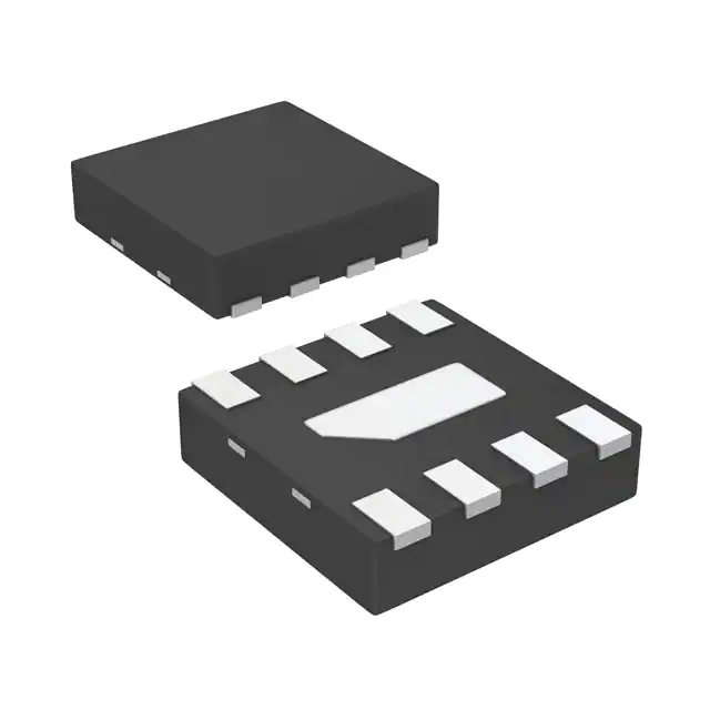
The device is packaged in 8-pin QFN package measuring
0.55mm(H) x 2mm(W) x 2mm(L).
- LED pulse width control
- Low shut down current
- External LED drive-current control
• Complete shutdown mode
• Supply voltage : 2.4 V to 3.6 V
• Operational in sunlight conditions up to 100klux(with
HSDL-9100)
• Artificial light immunity
• Analog & Digital output available
- Built in hysteresis comparator for digital output
• LED stuck High protection
• Wide bandwidth Trans-impedance amplifier
• External capacitor and resistor for integration and gain
controls
• Flexibility to enhance detection distance up to 200mm
with HSDL-9100 or further with external discretes pair
• Small 2mm x 2mm QFN 8-pin package
• Design flexibility to pair with Avago Proximity Sensors
or discretes pair solution
• Lead-free & ROHS Compliant
Applications
• PDA and mobile phones
Ordering Information
• Portable and Handheld devices
Part Number
Package
Shipping Option
• Personal Computers/Notebooks
APDS-9700-020
Tape & Reel
2500
• Amusement/Games/Vending Machines
• Industrial Automation
Application Support Information
• Contactless Switches
The Application Engineering Group is available to assist
you with the application design associated with APDS9700 module. You can contact them through your local
sales representatives for additional details.
• Sanitary Automation
�Absolute Maximum Ratings (Ta=25°C)
Parameter
Symbol
Min.
Max.
Units
Supply Voltage
VCC
0
4.5
V
Input Logic Voltage
Vi
0
4.5
V
260
°C
Reflow Soldering Temperature
Conditions
Recommended Operating Conditions
Parameter
Symbol
Min.
Max.
Units
Conditions
Operating Temperature
TA
-40
105
°C
Storage Temperature
Ts
-40
125
°C
Supply Voltage
VCC
2.4
3.6
V
Symbol
Minimum
Typical
Logic High Voltage, LEDON
VIH
1.6
Vcc
V
Logic High Voltage, ENB
VIH
1.4
Vcc
V
For Vcc = 2.4V
1.5
Vcc
V
For 2.4V < Vcc ≤ 3V
1.7
Vcc
V
For 3V < Vcc ≤ 3.6V
Electrical & Optical Specifications (Ta=25°C)
Parameters
Maximum Units
Conditions
Input
Logic Low Voltage, LEDON
VIL
0
0.3
V
Logic Low Voltage, ENB
VIL
0
0.3
V
Logic High Input Current, LEDON
IIH
0.1
1
uA
VI ≥ VIH
Logic High Input Current, ENB
IIH
0.1
1
μA
VI ≥ VIH
Logic Low Input Current, LEDON
IIL
0.1
1
μA
VI ≤ VIL
Logic Low Input Current, ENB
IIL
0.1
1
μA
VI ≤ VIL
Shutdown Current
ISD
0.3
1
μA
Vcc=3V, ENB=3V
Idle Current
Icc
500
650
μA
Vcc=3V, ENB=0V
0.3
V
IDOUT(Low) = 2mA, Vcc = 3V
Output
Digital Output
VOL
0
Rise Time(DOUT)
TR
1
us
Vcc = 3V, R2 = 10kΩ, Frequency = 10kHz
Fall Time(DOUT)
TF
1
us
Vcc = 3V, R2 = 10kΩ, Frequency = 10kHz
Rise Time (LEDA)
TR
40
ns
Vcc = 3V , ILED = 120mA, Freq = 10kHz
Fall Time (LEDA)
TF
40
ns
Vcc = 3V , ILED = 120mA, Freq = 10kHz
Max ILED Pulse Width
Max-PW
120
μs
Vcc=3V, ENB=0V
ILED Pulse Current
ILED
120
mA
Vcc=3V, R1 = 10Ω
Transmitter
�
300
�Electrical & Optical Specification (continued)
Parameters
Symbol
Minimum
Typical
Maximum Units
Conditions
Photodiode input current (PD)
IPD
0
Current Gain
IPFiLT/IPD
20
times Vcc = 3V
Hysterisis
VHYS
40
mV
Vcc= 3.0V
Threshold voltage
V TH
655
mV
Vcc= 3.0V
IDC
100
μA
Vcc= 3.0V
Receiver
3
μA
Hysterisis Comparator
Sunlight Cancellation
DC Current, PD
APDS-9700 pin-out and I/O Configurations
PIN #1
CORNER
Pin 1
Pin 8
Pin 2
Pin 7
Pin 3
Pin 6
Pin 4
Pin 5
I/O Pins Configuration Table
Pin
Symbol
Type
Description
1
LEDON
Digital I/P
LED Driver Input
LEDA will turn off when LEDON is stuck in high state for > Max-PW
2
ENB
Digital I/P
Power Down Enable
ENB = 0 Normal mode operation
ENB = 1 Shut down mode
3
DOUT
Digital O/P Digital Output
An open drain output that requires a pull-up resistor of recommended value 10k Ω
DOUT = 0 when VPFILT > V TH
DOUT = Vcc when VPFILT < V TH
4
GND
Ground
Ground
5
PD
Analog I/P
Photo-Detector Input
Connect to Cathode of photo-detector (proximity sensor)
6
PFILT
Analog O/P Analog Output
Connect to integration circuit (R3 & CX3)
7
LEDA
Analog O/P LED Driver Output
Connect to Anode of LED (proximity sensor)
LEDA will turn off when LEDON is stuck in high state for > Max-PW
8
VCC
Supply
�
Voltage Supply
�VIO
R2
PWM/
GPIO
LEDON
GPIO
1
8
Vcc
ENB
R1
2
MCU
7
LEDA
APDS-9700
GPIO
CX2
CX1
DOUT
3
R3
6
PFILT
CX3
GND
ADC
4
5
PD
Avago
Proximity Sensor
Reflective Object
Figure 1. Typical Application Circuit for APDS-9700
Recommended Avago Proximity Sensor
Description
HSDL-9100
Integrated Reflective Proximity Sensor
Component
Recommended Values ( with HSDL-9100)
R1
10 Ω
R2
10k Ω
R3
100k Ω to 500k Ω
CX1
100 nF ± 20% X 7R, Ceramic,
CX2
6.8 μF ± 20%, Tantalum
CX3
3.3 nF ± 20% X 7R, Ceramic
�
�APDS-9700 Block Diagram
(1) LEDON
(7) LEDA
Stuck High
Protection
Sunlight
Cancellation
R1
(5) PD
TIA
V IO
Avago
Proximity Sensor
PIN
(6) PFILT
R2
CX3
V-I CONVERTER
(2) ENB
(3) DOUT
Hysteresis
Comparator
(4) DOUT
Figure 2. APDS-9700 Block Diagram
�
LED
R3
�APDS-9700 Package Dimensions
2
7
6
5
1
2
3
4
2
8
PIN #1 ID ON TOP
0.05
0.15
0.05
0.50
0.55
TOP VIEW
0.7
2
1.3
R0.1
0.7
0.65
1.35
1
0.22
0.35
SIDE VIEW
R0.125
0.35
0.25
0.25
0.5
0.75
BOTTOM VIEW
Dimensions in mm. Tolerance ±0.1mm
Figure 3. Package Outline Dimensions and land patterm
�
�APDS-9700 Tape and Reel Dimensions
0.254±0.02
Ko = 1.00 ±0.05 ±0.05
4.00±0.10
4.00±0.10
2.00 ±0.05
ø1.50 ±0.10
1.75 ±0.10
+0.30 / -0.10
8.00 \ S
3.50 ±0.05
Bo = 2.30 ±0.05 ±0.05
Ao = 2.30 ±0.05
ø1.00 +0.25/-0.00
10º MAX
Unit Orientation Package
YWW
Figure 4. APDS-9700 Tape and Reel Dimensions
Marking Information
The unit is marked ‘YWW’ on the chip.
Y = Year
WW= work week
�
Note:
1. All unit are in millimeters
2. General Tolerance: Specified
3. Resistivity: 50ns
Burst Pulses
LEDON
>20µs
PFLIT
V TH
DOUT
Note:
Pulses at LEDON can only be activated at least 20us after ENB turn from high to low.
10
�APDS-9700 Performance Charts (Typical Conditions)
1.6
1.1
1.4
1
NORMALIZED ILED
NORMALIZED ILED
1.2
1
0.8
0.9
0.8
0.7
0.6
0.6
0.4
0.2
0.5
2.4
2.6
2.8
3
VCC (V)
3.2
3.4
-40
3.6
Figure 8. Normalized ILED Vs Vcc (T=25 °C, R1=10Ω )
-20
0
20
40
TEMP(ºC)
60
80
100
Figure 9. Normalized ILED VS Temp (VCC=3V,R1=10Ω)
1.1
0.7
Vcc=2.4V
0.6
Vcc=3V
1.05
0.5
TYPICAL ILED (A)
NORMALIZED ICC IDLE
Vcc=2.7V
1
Vcc=3.3V
Vcc=3.6V
0.4
0.3
0.2
0.95
0.1
0.9
2.4
2.6
2.8
3
VCC(V)
3.2
3.4
1.2
1.02
1.15
1.01
1.1
1.00
1.05
1
0.95
0.9
3
4
5
6
RLED (-)
7
8
9
10
0.99
0.98
0.97
0.96
0.95
0.85
0.8
2.4
2
Figure 11. ILED VS RLED (T=25°C)
NORMALIZED ICC IDLE
NORMALIZED ICC SD
Figure 10. Normalized ICC Idle Vs Vcc (T=25°C)
0.94
2.6
2.8
3
VCC(V)
Figure 12. Normalized ICC SD VS VCC (T=25°C)
11
0
3.6
3.2
3.4
3.6
0.93
-40
-20
0
20
40
TEMP(ºC)
Figure 13. Normalized ICC IDLE VS TEMP (VCC=3V)
60
80
100
�Appendix A: SMT Assembly Application Note
Recommended Minimum Land pattern and Keep-out Area
1. Area of Solder Land pattern = 2.3mm x 2.1mm
0.32
0.5
0.1
Keep-out Area Recommendations:
2. Module placement tolerance & keep out on each side
with no lead = 0.55mm & keep out on each side solder
lead = 0.8mm
0.25
0.22
R0
.17
5
2
0.22
3. Keep-out area = 3.9mm x 3.2mm
0.25
0.5
2
SOLDER LAND PATTERN
Dimension in mm. Tolerances +0.1mm
For product information and a complete list of distributors, please go to our web site:
www.avagotech.com
Avago, Avago Technologies, and the A logo are trademarks of Avago Technologies in the United States and other countries.
Data subject to change. Copyright © 2005-2008 Avago Technologies. All rights reserved.
AV02-0893EN - August 13, 2008
�
很抱歉,暂时无法提供与“APDS-9700-020”相匹配的价格&库存,您可以联系我们找货
免费人工找货- 国内价格
- 5+16.17269
- 50+15.76655
- 100+15.37291
- 1000+14.99176
- 2000+14.61478


 工商网监
湘ICP备2023018690号
工商网监
湘ICP备2023018690号
