APDS-9702
Signal Conditioning IC for Optical Proximity Sensors
with Digital I2C Interface
Data Sheet
Description
Features
APDS-9702 is a signal conditioning IC that enhances the
performance and robustness of the optical sensors used
for proximity or object detection.
x Low power consumption
– Internal oscillation circuit to drive LED in pulse
mode
– Low shut down current
– External LED drive-current control
APDS-9702 is a single chip solution that consists of an I2C
Write function, oscillation circuit, LED driver circuit and
sunlight cancellation circuit integrated into a single chip.
APDS-9702 has artificial light immunity and is also operational under the sun. Design flexibility is optimized as
APDS-9702 can be paired up with an integrated proximity
sensor or discrete pair solution.
APDS-9702 can be disabled to maximize power savings
and battery life in applications such as portable or battery-operated devices. The LED current of the optical
proximity sensors can be configured to different levels
using a limiting resistor at the LEDA pin. APDS-9702 also
provides user options in frequency, suitable burst rate,
comparator threshold setting and burst off period that can
reduce power consumption. These low power consumption features makes it also ideal for low power mobile and
handheld devices.
APDS-9702 is capable of operating at voltage supply
ranging from 2.4 V to 3.6 V. APDS-9702 has two separate
output pins for analog and digital outputs. This provides
flexibility to use either the analog or digital output (or
both) depending on the requirements of the application.
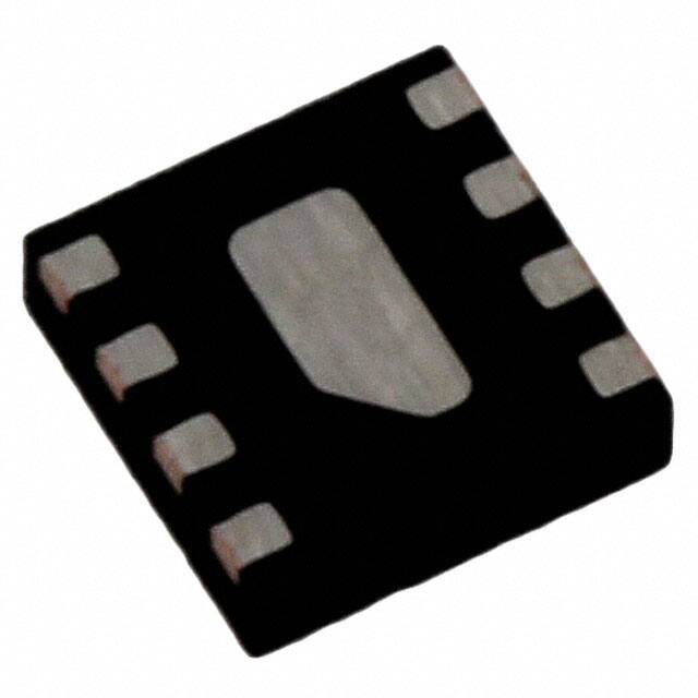
The device is packaged in 8-pin QFN package measuring
0.55mm(H) x 2mm(W) x 2mm(L).
x Complete shutdown mode
– Low shutdown current
x Supply voltage : 2.4 V to 3.6 V
x Operational in sunlight conditions up to 100klux(with
HSDL-9100)
x Artificial light immunity
x Analog & Digital output available
– Built in comparator for digital output
– Digital output remains Low during object detected.
x Wide bandwidth Trans-impedance amplifier
x External capacitor and resistor for integration and gain
controls
x Flexibility to enhance detection distance up to 200mm
with HSDL-9100 or further with external discrete pair
x Small 2mm x 2mm QFN 8-pin package
x Design flexibility to pair with Avago Proximity Sensors
or discrete pair solution
x Lead-free & RoHS Compliant
Applications
x PDA and mobile phones
Ordering Information
x Digital Camera
Part Number
Packaging
Quantity
x Portable and Handheld devices
APDS-9702-020
Tape & Reel
2500 per reel
x Personal Computers/Notebooks
x Amusement/Games/Vending Machines
Application Support Information
x Industrial Automation
The Application Engineering Group is available to
assist you with the application design associated with
APDS-9702 module. You can contact them through your
local sales representatives for additional details.
x Contactless Switches
x Sanitary Automation
�APDS-9702 Block Diagram
VCC
(8) VCC
Rp
Rp
(7) LEDA
Timing
Control
(1) SDA
I2C
(2) SCL
Sunlight
Cancellation
Oscillator
R1
Avago
Proximity Sensor
(5) PD
TIA
VCC
R2
(6) PFILT
CX3
V-I Converter
(3) DOUT
+
Latch
Comparator
100k 300k 500k
(4) GND
Figure 1. APDS-9702 Block Diagram
2
LED
PIN
R3
(Optional)
�APDS-9702 pin-out and I/O Configurations
PIN #1
CORNER
Pin 1
Pin 8
Pin 2
Pin 7
Pin 3
Pin 6
Pin 4
Pin 5
I/O Pins Configuration Table
Pin
Symbol
Type
Description
1
SDA
Digital I/O
I2C Serial Data I/O terminal
2
SCL
Digital I/P
I2C input / output signal
I2C Serial Clock Input terminal
I2C clock input signal
3
DOUT
Digital O/P
Digital Output
An open drain output that requires a pull-up resistor of recommended value 10k :
DOUT = Low at last LED pulse of burst when VPFILT > V TH, DOUT remains Low during
object detected.
DOUT = High at last LED pulse of burst when VPFILT < V TH, DOUT remains High during
object not detected.
Please refer to Output Waveforms Definition.
4
GND
Ground
Ground
5
PD
Analog I/P
Photo-Detector Input
Connect to Cathode of photo-detector (proximity sensor)
6
PFILT
Analog O/P
Analog Output
Connect to integration circuit (R3 & CX3)
7
LEDA
Analog O/P
LED Driver Output
Connect to Anode of LED (proximity sensor)
8
VCC
Supply
Voltage Supply
Absolute Maximum Ratings
Parameter
Symbol
Min.
Max.
Units
Conditions
Supply Voltage
VCC
0
3.6
V
Ta=25°C
Input Logic Voltage
VI
0
3.6
V
Ta=25°C
260
°C
Reflow Soldering Temperature
Recommended Operating Conditions
Parameter
Symbol
Min.
Max.
Units
Operating Temperature
TA
-40
85
°C
Storage Temperature
TS
-40
125
°C
Supply Voltage
VCC
2.4
3.6
V
3
Conditions
�Electrical & Optical Specifications (Ta=25°C)
Parameters
Input
Symbol
Minimum
Logic High Input Voltage
VIH
0.7*VCC
Logic Low Input Voltage
VIL
Typical
Maximum
Units
Conditions
V
0.3* VCC
V
Logic High Input Current
IIH
0.1
PA
VI ≥ VIH
Logic Low Input Current
IIL
0.1
PA
VI ≤ VIL
Shutdown Current
ISD
Standby Current
ISB
70
1
PA
Vcc = 3.0 V, TRG = X, PWR = 0
100
PA
Vcc = 3.0 V, TRG = 0, PWR = 1
0.3
V
IDOUT(Low) = 2 mA, Vcc = 3.0 V
V
:
Vcc = 3.0 V, R2 = 10k:
mA
Vcc = 3.0 V, R1 = 10:
Output
Digital Output Low Level
VOL
0
Digital Output High Level
VOH
Vcc – 0.3
Built-in Resistor at PFILT
RFILT
100k, 300k,
500k
ILED
125
Through I2C set.
Transmitter
ILED Pulse Current
Number of LED Pulse
16 x (1, 2, …,
16 times)
LED Pulse Frequency
12.5, 25, 50,
100
LED Burst Duration vs.
OFF Period
1/16, 1/64,
1/128, 1/256
235
Through I2C set.
kHz
Through I2C set.
Pulse Duty Cycle = 50%.
Through I2C set.
Receiver
0
3
PA
Photodiode Input
Current (PD)
IPD
Current Gain
IPFILT/IPD
20
times
Vcc = 3.0 V [1]
V TH
0.12
0.17
0.22
0.27
0.32
0.37
0.42
0.47
0.52
0.57
0.62
0.67
0.72
0.77
0.82
0.87
V
TH = 0000,
TH = 0001,
TH = 0010,
TH = 0011,
TH = 0100,
TH = 0101,
TH = 0110,
TH = 0111,
TH = 1000,
TH = 1001,
TH = 1010,
TH = 1011,
TH = 1100,
TH = 1101,
TH = 1110,
TH = 1111
IDC
100
PA
Vcc = 3.0 V[1]
Comparator Threshold
Threshold voltage
Sunlight Cancellation
DC Current, PD
Note:
1. Specified by design, not production tested.
4
�Typical Application Circuit
VCC
Rp
Rp
R2
SDA
SDA
1
8
VCC
CX1
SCL
SCL
2
7
LEDA
CX2
R1
R3 (Optional)
MCU
DOUT
GPIO
APDS-9702
3
6
PFILT
CX3
(Optional)
GND
ADC
4
5
Avago
Proximity Sensor
PD
Reflective Object
Figure 2. Typical Application Circuit for APDS-9702
Recommended Avago
Proximity Sensor
Description
HSDL-9100
Integrated Reflective Proximity Sensor
Component
Recommended Values ( with HSDL-9100)
R1
10 : ± 5%, 0.25W
R2
10k: ± 5%
R3
1M: ± 5%
Rp
10k: ± 5%
CX1
100 nF ± 20% X 7R, Ceramic,
CX2
6.8 PF ± 20%, Tantalum
CX3
3.3 nF ± 20% X 7R, Ceramic
5
�I2C Definition
APDS-9702 operates as slave device on I2C bus for clock frequency (SCL) up to 400 kHz. The basic protocol of I2C bus is
described below, for more details and specifications, please refer to I2C-bus specification and user manual.
SDA
SCL
S
P
START condition
STOP condition
START and STOP conditions
P
SDA
MSB
acknowledgement
signal from slave
MSB
acknowledgement
signal from receiver
MSB
SCL
1
S or Sr
2
7
START or
repeated START
condition
8
1
9
ACK
byte complete,
interrupt within slave
2
3 to 8
9
ACK
1
2
3 to 8
9
ACK
clock line held LOW while
interrupts are serviced
Sr
Sr or P
STOP or
repeated START
condition
Data transfer on I2C bus
SDA
SCL
1-7
8
9
1-7
8
9
1-7
8
9
P
S
START
condition
ADDRESS
W
ACK
DATA
Low byte
ACK
DATA
High byte
ACK
STOP
condition
A complete data transfer
1
7
1
1
8
1
8
1
1
S
Slave Address
Wr
A
Data Byte
A
Data Byte
A
P
S
Start Condition
Wr
Write”0”
A
Acknowledge (0 for ACK)
P
Stop Condition
Master-to-Slave
Slave-to-Master
Slave Address: 1010100 (Default)
6
�Register Definition
Bit
Default
15
14
13
12
11
10
9
8
7
6
5
4
3
2
1
0
TRG
PWR
NB3
NB2
NB1
NB0
F1
F0
DC1
DC0
TH3
TH2
TH1
TH0
R1
R0
0
0
0
0
0
1
0
0
1
0
0
1
0
0
0
0
Register
Type
Description
TRG
Trigger
This pin is active high.
TRG = 1 o Normal proximity sensing operations
TRG = 0 o No operation (Default)
PWR
Power
PWR = 0 o Power Shut Down (Default)
PWR = 1 and TRG = 0 o Standby
PWR = 1 and TRG = 1 o Active Operations
NB
NBurst
Number of LED Pulse per Burst = 16 x (1, 2, …, 16 times);
0x0 = 16-pulse, 0x1 = 32-pulse (Default), …, 0xE = 240-pulse,
0xF = 256-pulse
Figure 3
F
Frequency
00 = 12.5kHz (Default), 01 = 25kHz, 10 = 50kHz, 11 = 100kHz;
Wave is fixed at 50% Duty Cycle
Figure 3
DC
Duration Cycle
LED Burst Duration versus OFF period;
00 = 1:16, 01 = 1:64, 10 = 1:128 (Default) and 11 = 1:256
Figure 3
TH
Threshold,
VTH
16 options of Comparator Threshold Setting;
0000 = 0.12V, 0001 = 0.17V, 0010 = 0.22V, 0011 = 0.27V,
0100 = 0.32V (Default), 0101 = 0.37V, 0110 = 0.42V, 0111 = 0.47V,
1000 = 0.52V, 1001 = 0.57V, 1010 = 0.62V, 1011 = 0.67V,
1100 = 0.72V, 1101 = 0.77V, 1110 = 0.82V, 1111 = 0.87V
Figure 4
R
RFLIT
Programmable Filter Register;
00 = No resistor (Default), 01 = 100k, 10 = 300k, 11 = 500k
Figure 5
50% DC
Number of LED Pulses
LED Burst Duration
Figure 3. LEDA Burst Pulses Definition
7
Remark
Burst Pulse OFF Period
Duration Cycle = LED Burst Duration:
Burst Pulse OFF Period
�Transmit Burst Pulses Definition
Operation ON/OFF condition is shown in the following table:
TRG
PWR
Condition
X
0
Shut down
0
1
Standby Mode
1
1
Active Mode, pulses sent
The burst pulses at LEDA pin will be activated under 2 state conditions with 2 different start-up timing. The following
diagrams explained these 2 scenarios.
(a) State condition 1:
From Shut down -> Standby Mode -> Active Mode: Burst pulses at LEDA pin are activated after 1.3 ms
LEDA Burst Pulses
I2C
Shutdown
I2C
Standby
I2C
Active
>1.3 ms
(b) State condition 2:
From Shut down -> Active Mode: Burst pulses at LEDA pin are activated after 1.3 ms
LEDA Burst Pulses
I2C
Shutdown
I2C
Active
>1.3 ms
8
�Output Waveforms Definition
Burst Pulses
LEDA
VTH
PFILT
Object detected
DOUT
Figure 4. Output Waveforms Definition
9
Object detected
Object not detected
No object detected
�RFILT Definition
There are built-in resistors at PFILT (pin 6) to provide 4 options to set the desired resistor for integrated RC circuit.
R0
R1
Resistor Value
0
0
Open. External resistor R3 is required to be in parallel with CX3
0
1
100k ohm. R3 become optional.
1
0
300k ohm. R3 become optional.
1
1
500k ohm. R3 become optional.
(6) PFILT
V-I Converter
+
Comparator
100K
300K
500K
(4) GND
Figure 5. RFILT definition
10
CX3
R3 (Optional)
�APDS 9702 Performance Charts
RELATIVE LED CURRENT VS VCC
1.60
1.40
RELATIVE LED CURRENT
RELATIVE LED CURRENT
1.40
1.20
1.00
0.80
0.60
0.40
0.20
0.00
2.2
2.6
2.8
3
VCC (V)
3.2
3.4
3.6
0.80
0.60
0.40
-60
3.8
RELATIVE ICC STANDY CURRENT VS VCC
-40
-20
0
20
40
TEMPERATURE (°C)
60
80
100
RELATIVE STANDBY CURRENT VS TEMPERATURE
1.20
1.00
1
RELATIVE ICC STANDBY
RELATIVE ICC STANDY CURRENT
1.00
0.00
2.4
0.8
0.6
0.4
0.2
0.80
0.60
0.40
0.20
0.00
0
2.2
2.4
2.6
2.8
3
3.2
VCC (V)
3.4
3.6
3.8
AVERAGE PEAK LED CURRENT VS R1
300
PEAK LED CURRENT (mA)
1.20
0.20
1.2
250
200
VCC
3.3V
3.0V
2.7V
2.4V
150
100
50
0
11
RELATIVE LED CURRENT VS TEMPERATURE
1.60
0
2
4
6
R1 (OHMS)
8
10
12
-60
-40
-20
0
20
40
TEMPERATURE (°C)
60
80
100
�APDS-9702 Package Dimensions
QFN 8-Pin Package
2
7
6
5
1
2
3
4
2
8
Pin #1 ID On Top
0.02
0.50
0.10
TOP VIEW
SIDE VIEW
1.20
0.28
0.40
2
3
4
8
7
6
5
0.60
0.7
1
0.35 X 45°
0.125 (x4)
0.25 (x8)
0.25 (x6)
BOTTOM VIEW
Note:
1. All Dimensions in mm. Tolerance ±0.1mm unless specified.
2. Marking Information:
The unit is marked ‘YWW LLa’ on the chip.
Y = Year (Last digit of the year)
WW = work week (1-54)
LL = Lot number (01-99)
a
= Denote this is an I2C part.
12
�0.1
0.32
0.5
Recommended Minimum Land pattern and Keep-out Area
Keep-out Area Recommendations:
0.22
R0
.17
5
2
2.2
Area of Solder Land pattern = 2.3mm x 2.1mm
Module placement tolerance & keep out on each side with
no lead = 0.55mm & keep out on each side solder lead =
0.8mm
Keep-out area = 3.9mm x 3.2mm
0.25
0.25
0.5
2
SOLDER LAND PATTERN
Dimension in mm.
Recommended tolerances +/-0.1mm
13
�APDS-9702 Tape and Reel Dimensions
Tape Dimensions
4.00 ± 0.10
2.00 ± .05
Ø 1.50 + .10
4.00 ± 0.10
1.75 ± 0.10
3.50 ± .05
.30
8.00 + .10
Ø 1.00 + 0.25
YWW
LLa
UNIT ORIENTATION
IN POCKET
.254 ± 0.02
5° MAX
5° MAX
2.30 ± 0.10
A.
0.75 ± 0.10
K.
ALL DIMENSIONS IN mm.
14
2.30 ± 0.10
B.
�Reel Dimensions
W3
(INCLUDES FLANGE
DISTORTION AT
OUTER EDGE)
W2
(MEASURE
AT HUB)
B
W1
(MEASURE
AT HUB)
ø60.0 ± 0.5
ø56.8 ± 0.5
A
A
øN
R12.7
øA
60°
E
R75.0
REEL MADE IN MALAYSIA
1.6
SEE DETAIL A
11.3
1.6
1.9
FRONT VIEW
B
SECTION: BB
BACK VIEW
1.5 MIN
0.5
ø13.0 ±0.2
ø20.2 MIN
SECTION: AA
ARBOR HOLE
DETAIL A
SCALE 2:1
Product SPecifications
TAPE WIDTH
ØA
08MM
180 –2.0
+0.0
ØN
WT
60 ±2.0
8.4 –0.0
+1.5
W2
(MAX)
W3
14.4
8.4 –0.5
+2.5
E
4.0 ± 0.1
All Dimensions in mm.
Packaging
All APDS-9702 options are shipped in ESD proof packaging.
This part is compliant to JEDEC MSL 1.
Recommended Storage Conditions
Storage Temperature
The units in tape and reel are recommended to be kept in a controlled climate
environment, with temp at 25 +5/-10°C and relative humidity at 55 +/-15%.
Time from unsealing to soldering
This part is compliant to JEDEC MSL-1 (unlimited floor life at < 30°C / 85%RH)
15
�Recommended Reflow Profile
MAX 260C
T - TEMPERATURE (°C)
255
R3
230
217
200
180
150
120
R2
R4
60 sec to 90 sec
Above 217 C
R5
R1
80
25
0
50
P1
HEAT
UP
100
150
P2
SOLDER PASTE DRY
The reflow profile is a straight-line representation of
a nominal temperature profile for a convective reflow
solder process. The temperature profile is divided into
four process zones, each with different 'T/'time temperature change rates or duration. The 'T/'time rates or
duration are detailed in the above table. The temperatures
are measured at the component to printed circuit board
connections.
In process zone P1, the PC board and APDS-9702 pins are
heated to a temperature of 150°C to activate the flux in
the solder paste. The temperature ramp up rate, R1, is
limited to 3°C per second to allow for even heating of both
the PC board and APDS-9702 pins.
Process zone P2 should be of sufficient time duration (100
to 180 seconds) to dry the solder paste. The temperature is
raised to a level just below the liquidus point of the solder,
usually 200°C (392°F).
200
P3
SOLDER
REFLOW
250
P4
COOL DOWN
300
t-TIME
(SECONDS)
Process zone P3 is the solder reflow zone. In zone P3, the
temperature is quickly raised above the liquidus point of
solder to 255°C (491°F) for optimum results. The dwell time
above the liquidus point of solder should be between 20
and 40 seconds. It usually takes about 20 seconds to assure
proper coalescing of the solder balls into liquid solder
and the formation of good solder connections. Beyond a
dwell time of 40 seconds, the intermetallic growth within
the solder connections becomes excessive, resulting in
the formation of weak and unreliable connections. The
temperature is then rapidly reduced to a point below the
solidus temperature of the solder, usually 200°C (392°F), to
allow the solder within the connections to freeze solid.
Process zone P4 is the cool down after solder freeze. The
cool down rate, R5, from the liquidus point of the solder to
25°C (77°F) should not exceed 6°C per second maximum.
This limitation is necessary to allow the PC board and
APDS-9702 pins to change dimensions evenly, putting
minimal stresses on the APDS-9702.
It is recommended to perform reflow soldering no more
than twice.
For product information and a complete list of distributors, please go to our web site:
www.avagotech.com
Avago, Avago Technologies, and the A logo are trademarks of Avago Technologies in the United States and other countries.
Data subject to change. Copyright © 2005-2010 Avago Technologies. All rights reserved.
AV02-2238EN - March 3, 2010
�


 工商网监
湘ICP备2023018690号
工商网监
湘ICP备2023018690号
