APDS-9801
Digital Proximity and Analog Ambient Light Sensor
Data Sheet
Description
Features
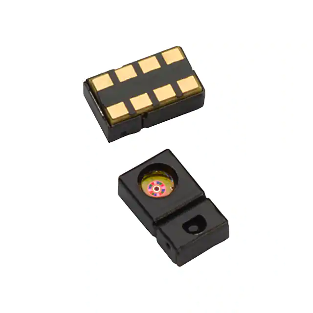
APDS-9801 is a module that integrates functions of an
Analog ambient light sensor (ALS) and a proximity sensor
(PS). The sensor has four chips in one small package: an
ambient light sensor IC, proximity sensor signal conditioning circuitry and a proximity sensor that includes both an
emitter and detector. The Analog ambient light sensor
has current output, with spectral response close to the CIE
standard Photopic observer. The proximity sensor IC has a
LED driver and receiver circuit with digital count output,
featuring excellent ambient light cancellation capability. With the built-in LED, the proximity sensor is able to
sense the proximity of an object, such as finger or head to
a portable device.
x Integrated module with built-in IR LED, IR Detector,
Digital Signal Conditioning ASIC and Analog ALS
Ambient light sensors can be used to control the brightness of display backlighting by detecting the ambient
light illuminance level. Proximity sensor technology make
possible applications where detection or proximity of a
user’s head in relationship to display will turn off/on the
keypad and LCD backlight. The combination of ambient
light sensors and proximity sensors in one module make
it ideal for portable devices, such as mobile phone, PDA
and notebooks.
x Package size: L 6.1 x W 3.9 x H 1.75 mm
x Sensor power supply voltage range: 1.7 V to 2.5 V
x I2C Bus power supply voltage range: 1.7 V to 3.6 V
x Broad VLED range for PS: 2.5 V to 5V
x PS Shutdown Current 1PA Typical
x ALS approximate the Human Eye response
x Low sensitivity variation across various light sources
x ALS Output linearity up-to 5k Lux range
x Operational under sunlight (PS)
x Artificial light Immunity
x Low crosstalk between Emitter & Detector
x Programmable LED driving current and burst pulse
control (PS)
x Interrupt logic with Programmable Threshold
x Lead-free & ROHS Compliant
Applications
x PDA and mobile phones
Ordering Information
Part Number
Packaging Type
Quantity
x Portable and Handheld devices
APDS-9801
Tape and Reel
2500 per reel
x Personal Computers/Notebooks
x Amusement/Games/Vending Machines
x Contactless Switches
�Functional Block Diagram
8-VLED
7–PS-INTR
6-IOUT
5-SDA
OSC
LED
Driver
I2C
Interfacing
Control & Digital
Logic
³ADC
(12 bit)
Pre-Amp
Current
Amplifier
GND
1-NC
2-VDD
3-GND
4-SCL
I/O Pins Configuration Table:
Pin
SYMBOL
Description
1
NC
No Connect
2
VDD
Power Supply Pin
3
GND
Ground
4
SCL
I2C Clock Input
5
SDA
I2C Data Input/Output
6
IOUT
ALS Output Current
7
PS-INTR
Output pin for PS Level Interrupt
8
VLED
Power Supply pin for LED. Connect this pin to V-Battery or Power supply
Absolute Maximum Ratings
Parameter
Symbol
Min
Max
Unit
Conditions
Supply Voltage
VDD
-0.5
4
V
TA = 25°C
Voltage at I/O pins
VIO
-0.5
TA = 25°C
Reflow Soldering Temperature
TS
5
V
260
°C
Recommended Operating Conditions
Parameter
Symbol
Min
Max
Unit
Operating Temperature
TA
-40
70
ºC
Storage Temperature
TS
-40
85
ºC
Supply Voltage
VDD
1.7
2.5
V
I2C Bus Power Supply Voltage
VBUS
1.7
3.6
V
PS LED Power Supply Voltage
VLED
2.5
5
V
2
Condition
�Electrical & Optical Specifications (TA = 25°C)
Parameter
Symbol
ALS Output Current
IOUT
Min.
Unit
Conditions
83
PA
VDD=1.8 V, Ev=100 Lux, [1]
ALS Dark Current
300
nA
VDD=1.8 V, Ev=0 Lux
ALS Peak Spectral Sensitivity
560
nm
ALS Light Current Ratio
Typ.
Max.
[2]
1.1
ALS Saturation Voltage
VSAT
VDD-1.0
VDD-0.8
V
SCL, SDA Input High Voltage
VIH
1.25
SCL, SDA Input Low Voltage
VIL
0.54
V
INTR, SDA Output Low Voltage
(Open Drain) [PS]
VOL
0.3
V
ISINK=3 mA
0.6
V
ISINK=6 mA
Load=150 k:, VDD=1.8 V,
Ev=100 Lux, [1]
V
IAVG at 5 ms delay time
1.3
mA
VDD=1.8 V, IDD+ILEDAVG [3]
IAVG at 50 ms delay time
180
PA
VDD=1.8 V, IDD+ILEDAVG [4]
IAVG at 500 ms delay time
90
PA
VDD=1.8 V, IDD+ILEDAVG [5]
1
PA
VDD=1.8 V, Ev=0 Lux
1300
counts
Kodak 18% grey card, 30 mm
distance, Freq=100 kHz, n=20
pulses, Duty-cycle=25%,
ILED=100 mA, VDD=1.8 V, [6]
Refer to Figure 6.
nm
75, 100, 125, 150
mA
Programmable via I2C bus
PS-LED Pulse Frequency
50, 100, 200
kHz
Programmable via I2C bus
PS-Pulse Duty-Cycle
12.5%, 25%, 37.5%, 50%
Programmable via I2C bus
PS-Number of Pulses
4, 8, 12, 16, 20, 24, 28, 32
Programmable via I2C bus
PS-Burst Interval Delay
5, 20, 50, 125, 250, 500, 1000,
2000
Shutdown Current
ISD
PS Output Count
LED Peak Wavelength
PS LED - Output Current Peak
Full Scale ADC Count (PS)
Crosstalk (PS)
ILED
940
ms
Programmable via I2C bus
4092
counts
Programmable via I2C bus
250
counts
Freq=100kHz, n=20pulses,
Duty-cycle=25%, ILED=100mA,
VDD=1.8V, [7]
Note:
1. White LED is used as light source.
2. VDD=1.8 V, Current Light Ratio = (output current at 100 Lux Incandescent) / (output current at 100 Lux Fluorescent).
3. Test conditions: VDD=1.8 V, 5 ms delay, ILED=100 mA, 20 pulses, 25% duty cycle, Freq=100 kHz, Ev=0 Lux.
4. Test conditions: VDD=1.8 V, 50 ms delay, ILED=100 mA, 20 pulses, 25% duty cycle. Freq=100 kHz. Ev=0 Lux.
5. Test conditions: VDD=1.8 V, 500 ms delay, ILED=100 mA, 20 pulses, 25% duty cycle. Freq=100 kHz. Ev=0 Lux.
6. Test without window between sensor and grey card object.
7. Test without window or object above sensor.
3
�APDS–9801 Typical Application Circuit
VLED
C4
1-NC
VDD
VBUS
C3
R4
8-VLED
2-VDD
R3
R2
7 PS-INTR
GPIO
C2
APDS-9801
C1
3-GND
6-IOUT
ADC
R1
4-SCL
MCU
C5
5-SDA
SDA
SCL
R1
1 k: 1/16W 5%
R2, R3, R4
10 k: 5%
C1, C3
6.8 PF 10V
C2, C4
100 nF 10V
C5
10 PF 10V
4
�Definition of timing for I2C devices
This section will describe the main protocol of the I2C bus. For more details and timing diagrams, please refer to the I2C
bus specification.
SDA
tLOW
tf
tf
tSU;DAT
tr
tHD;STA
tSP
tr
tBUF
SCL
S
tHD;STA
tHD;DAT
tHIGH
tSU;STA
tSU;STO
Sr
P
S
MSC610
Characteristics of the SDA and SCL bus lines for I2C-bus devices
STANDARD-MODE
FAST-MODE
PARAMETER
SYMBOL
MIN.
MAX.
MIN.
MAX.
UNIT
SCL clock frequency
fSCL
0
100
0
400
kHz
Hold time (repeated) START condition.
After this period, the first clock pulse is generated
tHD;STA
4.0
–
0.6
–
Ps
LOW period of the SCL clock
tLOW
4.7
–
1.3
–
Ps
HIGH period of the SCL clock
tHIGH
4.0
–
0.6
–
Ps
Set-up time for a repeated START condition
tSU;STA
4.7
–
0.6
–
Ps
Data hold time:
tHD;DAT
300
–
300
–
ns
Data set-up time
tSU;DAT
250
–
100
–
ns
Rise time of both SDA and SCL signals
tr
–
1000
–
300
ns
Fall time of both SDA and SCL signals
tf
–
300
300
ns
Set-up time for STOP condition
tSU;STO
4.0
–
0.6
–
Ps
Bus free time between a STOP and START
condition
tBUF
4.7
–
1.3
–
Ps
Capacitive load for each bus line
Cb
–
400
–
400
pF
Noise margin at the LOW level for each
connected device (including hysteresis)
VnL
0.1VBUS
–
0.1VBUS
–
V
Noise margin at the HIGH level for each
connected device (including hysteresis)
VnH
0.2VBUS
–
0.2VBUS
–
V
5
�I2C Definition
Start and Stop conditions
SDA
SCL
S
P
START condition
STOP condition
Data transfer on I2C-bus
P
SDA
MSB
acknowledgement MSB
signal from slave
acknowledgement
signal from receiver
MSB
SCL
S or Sr
1
2
7
START or
repeated START
condition
9
ACK
8
1
2
3 to 8
9
ACK
1
2
3 to 8
clock line held LOW while
interrupts are serviced
byte complete,
interrupt within slave
A complete data transfer
SDA
SCL
1–7
8
9
1–7
8
9
1–7
8
9
P
S
START
condition
ADDRESS
R/W
ACK
DATA
DATA
ACK
STOP
condition
1
7
1
1
8
1
1
S
Slave Address
Wr/Rd
A
Data Byte
A
P
S
Start Condition
Wr
Write "0"
Rd
Write "1"
A
Acknowledge (0 for ACK or 1 for NACK)
P
Sr
Stop Condition
Repeated Start Condition
from Master to Slave
from Slave to Master
6
ACK
9
ACK
Sr
Sr or P
STOP or
repeated START
condition
�Write Byte Protocol
1
7
1
1
8
1
8
1
1
S
Slave Address
Wr
A
Common Code
A
Data Byte
A
P
Read Byte Protocol
1
7
1
1
8
1
1
7
1
1
8
1
1
S
Slave Address
Wr
A
Common Code
A
Sr
Slave Address
Rd
A
Data Byte
A
P
Slave Address
APDS-9801 PS slave address is 1010101 [0X55]
PS-I2C Interfacing
Register Address for PS:
ADDRESS
Register Name
Register Function
–
Command
Specifies register address
0h
Shutdown
Power on/off
1h
Pulse_Freq
Set the period, duty cycle and number of pulses for burst pulses
2h
Interval delay & control
Set the delay time between burst pulses & control
3h
Thres_low
Low byte of interrupt threshold
4h
Thres_high
High byte of interrupt threshold
5h
Data_low
Low byte of ADC output
6h
Data_high
High byte of ADC output
7h
interrupt
Interrupt status and enable
Command Register
The command register specifies the address of the target register for subsequence read and write operations. The write
byte protocol is used to configure the COMMAND register.
7
6
5
4
CMD
Threshold Interrupt clear
EOC Interrupt clear
Software Reset
3
2
1
Address
Reset Value: 0x00h
FIELD
BIT
Description
CMD
7
Select command register. Must be ‘1’
Threshold Interrupt clear
6
Clear the pending thresholds interrupt. Write ‘1’ to clear. Self clearing.
EOC Interrupt clear
5
Clear the pending end of conversion of the ADC interrupt. Write ‘1’ to clear. Self clearing.
Software Rest
4
Write 1 to this bit to reset the chip to default register value self clearing.
This is for software reset only.
ADDRESS
3:0
Register address. This field selects the specific register.
7
0
�Shutdown Register (0h)
7
6
5
4
3
2
1
0
shutdown
Reset value: 0x0h
FIELD
BIT
Description
Shutdown
0
0 for shutdown, oscillator and analog block all turn off
1 for turn on, measurement triggered by “start measurement” bit of interval delay/control register
Pulse_Freq Register (1h)
7
6
Pulse count
5
4
reserved
Reset value: 0x96h
FIELD
BIT
Description
Pulse count
7:5
Set the number of pulses for each burst.
000: 4 pulses
001: 8 pulses
010: 12 pulses
011: 16 pulses
100: 20 pulses (default)
101: 24 pulses
110: 28 pulses
111: 32 pulses
Duty cycle
3:2
Set the duty cycle of the burst pulse.
00: 12.5%
01: 25.0% (default)
10: 37.5%
11: 50.0%
Pulse frequency 1:0
8
Set the period for the burst pulse.
00: None
01: 50 kHz
10: 100 kHz (default)
11: 200 kHz
3
2
Duty cycle
1
0
Pulse frequency
�Interval Delay & Control Register (2h)
7
6
reserved
5
Start
Measurement
4
3
2
LED Current Control
1
0
Interval Delay
Reset value: 0x00h
FIELD
BIT
Description
Start Measurement
5
Write a “1” to this bit to enable measurement. By default this bit is ‘0’, no measurement.
LED Current Control
4:3
LED Current Control
00: 75 mA
01: 100 mA (default)
10: 125 mA
11: 150 mA
Interval Delay
2:0
Set the delay between the burst pulses.
000: 5ms
001: 20 ms
010: 50 ms
011: 125 ms
100: 250 ms
101: 500 ms (default)
110: 1s
111: 2s
Interrupt Threshold Register (Low byte) (3h)
7
6
5
4
3
2
1
0
Interrupt threshold low byte
Reset value: 0x00h
FIELD
BIT
Description
Interrupt threshold
Low byte
7:0
Lower byte of 12 bits Interrupt threshold. The 12 bit interrupt threshold values are expressed
as 12 bits values spread across 2 registers (register address 3h & 4h).
Interrupt Threshold Register (High byte) (4h)
7
6
5
reserved
4
3
2
1
0
Interrupt threshold low byte
Reset value: 0x00h
FIELD
BIT
Description
Interrupt threshold
High byte
3:0
Upper 4 bits of 12 bits Interrupt threshold. The 12 bit interrupt threshold values are expressed
as 12 bits values spread across 2 registers (register address 3h & 4h).
9
�ADC Data Output Register (Low byte) (5h)
7
6
5
4
3
2
1
0
ADC output data low byte
Reset value: 0x00h
FIELD
BIT
Description
ADC output data
Low byte
7:0
Lower byte of 12bits ADC output data. The ADC data are expressed as 12 bits values spread
across 2 registers (register address 5h & 6h). Read only.
ADC Data Output Register (High byte) (6h)
7
6
5
4
3
2
reserved
1
0
ADC output data high byte
Reset value: 0x00h
FIELD
BIT
Description
ADC output data high
byte
3:0
Upper 4 bits of 12 bits ADC output data. The ADC data are expressed as 12 bits values spread
across 2 registers (register address 5h & 6h). Read only.
Interrupt Register (7h)
7
6
5
4
resv
Negative
Threshold
interrupt status
Positive
Threshold
interrupt status
EOC interrupt
status
3
2
resv
1
0
Threshold
Interrupt enable
EOC Interrupt
enable
Reset value: 0x00h
FIELD
BIT
Description
Negative Threshold
interrupt status
6
Read only. Interrupt happens when ADC output data value fall below the interrupt threshold
set by threshold registers. Write a ‘1’ to bit 6 of the command register to clear the interrupt.
(note 2)
Positive Threshold
interrupt status
5
Read only. Interrupt happens when ADC output data value rise above the interrupt threshold
set by threshold registers. Write a ‘1’ to bit 6 of the command register to clear the interrupt.
(note 2)
EOC Interrupt status
4
Read only. Interrupt happens when it is the end of conversion for the ADC. Write a ‘1’ to bit 5
of the command register to clear the interrupt.
Threshold Interrupt
Enable
1
‘1’: threshold interrupt (when ADC rise above or fall below threshold set) enable to external
interrupt pin.
‘0’: threshold interrupt (when ADC rise above or fall below threshold set) disable to external
interrupt pin.
EOC Interrupt Enable
0
‘1’: EOC interrupt enable to external interrupt pin.
‘0’: EOC interrupt disable to external interrupt pin.
10
�Note 1: Figure 3 Definition of transmit burst pulses
1st burst
2nd burst
t
Pclk
N x pulses
Delay
Duty cycle = t/Pclk
Delay
= the time between the last burst pulse to the first burst pulse of the next burst
Note 2: Interrupt Status Implementation
The following diagram explained how the positive threshold interrupt status and negative threshold interrupt status is
implemented. ADC Data and Interrupt threshold is compared. The output is high or low depends on the comparison
result. The detection of rising edge of the comparator set the positive threshold interrupt status bit to ‘1’. The detection
of falling edge of the comparator set the negative threshold interrupt status bit to ‘1’.
ADC Data
+
Comparator Output
Interrupt Threshold
Comparator output waveform:
‘1’ if ADC Data > Interrupt Threshold
If rising edge is detected, Positive
Threshold interrupt status bit is set to ‘1’.
After reading the status bit, write ‘1’
to bit 6 of the command register to
clear the status. Wait for another
interrupt status assert.
11
‘0’ if ADC Data < Interrupt Threshold
If falling edge is detected, Negative
Threshold interrupt status bit is set to ‘1’.
After reading the status bit, write ‘1’
to bit 6 of the command register to
clear the status. Wait for another
interrupt status assert.
�PS – APPLICATION SOFTWARE
Configuration the registers
The Pulse_Freq register and Interval Delay and Control register are initialized to default values when power up. Setting
these registers to desired values would be part of setup procedure. The value can be change to optimize the performance need. Below are samples code illustrates the setting of registers for various option.
Set up Pulse_Freq
//20 pulses, 25% Duty Cycle and 100kHz Pulse Frequency
DeviceAddr = 0x55
//Slave address also be –or 0x55
Command = 0x81
//Set Command bit and address of Pulse_Freq
Value = 0x86
WriteByte_i2c(DeviceAddr, Command, Value)
//24 pulses, 50% Duty Cycle and 100kHz Pulse Frequency
DeviceAddr = 0x55
Command = 0x81
Value = 0x8E
WriteByte_i2c(DeviceAddr, Command, Value)
Set up Interval Delay and LED Current Control
//100mA of LED current and 5ms interval delay between the burst pulses
DeviceAddr = 0x55
//Slave address also be – 0x55
Command = 0x82
//Set Command bit and address of register
Value = 0x08
WriteByte_i2c(DeviceAddr, Command, Value)
//150mA of LED current and 250ms interval delay between the burst pulses
DeviceAddr = 0x55
Command = 0x82
Value = 0x1C
WriteByte_i2c(DeviceAddr, Command, Value)
Enable Measurement
DeviceAddr = 0x55
Command = 0x82
ReadByte_i2c(DeviceAddr, Command, & Value)
Value |= 0x20
WriteByte_i2c(DeviceAddr, Command, Value)
12
//Read back register value
//Set Enable Measurement bit
�PS – Interrupts
The interrupt feature of the device is simplifies and improves system efficiency by eliminating the need to poll the sensor
for proximity distance value. The feature may enable at Interrupt Register.
An interrupt will be happen when the values of ADC conversion value change from lower to upper or upper to lower over
the interrupt threshold value. Negative Threshold interrupt status show when ADC output values fall below interrupt
threshold from upper, and Positive Threshold interrupt status are vice versa.
End of ADC Conversion interrupt also can be use. An interrupt will be generated when completion of each conversion
of ADC.
Write ‘1’ to bit 6 of the command register to clear the threshold interrupt or write ‘1’ to bit 5 of the command register to
clear the End_of_Conversion interrupt.
Set up Threshold Interrupt
//Example threshold value = 0x1CA
//Write the interrupt threshold low byte
DeviceAddr = 0x55
Command = 0x83
Value = 0xCA
WriteByte_i2c(DeviceAddr, Command, Value)
//Write the interrupt threshold high byte
DeviceAddr = 0x55
Command = 0x84
Value = 0x01
WriteByte_i2c(DeviceAddr, Command, Value)
//Slave address also be – 0x55
//Set Command bit and addr of thresh low byte register
//Slave address also be – 0x55
//Set Command bit and addr of thresh high byte register
Enable Interrupt to external interrupt pin
//Enable Threshold interrupt
DeviceAddr = 0x55
Command = 0x87
Value = 0x02
WriteByte_i2c(DeviceAddr, Command, Value)
//Enable End_of_Conversion interrupt
DeviceAddr = 0x55
Command = 0x87
Value = 0x01
WriteByte_i2c(DeviceAddr, Command, Value)
//Set Command bit and addr of interrupt register
//Enable Threshold Interrupt
//Set Command bit and addr of interrupt register
//Enable EOC Interrupt
Clear the pending Interrupt
//Clear pending Threshold interrupt
DeviceAddr = 0x55
Command = 0x40
Write_i2c(DeviceAddr, Command)
//Slave address also be – 0x55
//Clear Threshold Interrupt
//Clear pending End of Conversion of the ADC Interrupt
DeviceAddr = 0x55
Command = 0x20
//Clear EOC Interrupt
Write_i2c(DeviceAddr, Command)
13
�Read ADC Data Output Values
//Read the ADC low byte channel and store at ADC_DataLow
DeviceAddr = 0x55
//Slave address also be – 0x55
//Set Command bit and addr of low byte of ADC Data output register
Command = 0x85
ReadByte_i2c(DeviceAddr, Command, &ADC_DataLow)
//Read the ADC high byte channel and store at ADC_DataHigh
//Set Command bit and addr of high byte of ADC Data output register
command = 0x86
ReadByte_i2c(DeviceAddr, Command, &ADC_DataHigh)
Software Examples
/**********************************************************************
Definitions
**********************************************************************/
#define
DeviceAddr
0x55
//Slave address for device
#define
#define
#define
#define
#define
#define
#define
#define
#define
CMD
ADDR_SD
ADDR_PFR
ADDR_ICR
ADDR_THRESLOW
ADDR_THRESHIGH
ADDR_ADCDATALOW
ADDR_ADCDATAHIGH
ADDR_INTP
0x80
0x00
0x01
0x02
0x03
0x04
0x05
0x06
0x07
//Command
//Shutdown Register address
//Pulse_Freq Register address
//Interval delay & Control Register address
//Threshold Low Register address
//Threshold High Register address
//ADC Data Output Low Register address
//ADC Data Output Low Register address
//Interrupt Register address
/**********************************************************************
Global Variable
**********************************************************************/
unsigned char PFR_Data;
//hold data of Pulse_Freq Register
unsigned char ICR_Data;
//hold data of Interval delay & Control Register
unsigned char ReadThresholdLow, ReadThresholdHigh
//read back threshold register value
unsigned char ADC_DataLow, ADC_DataHIGH
//read back ADC data
unsigned char IntSta;
//read back interrupt status
14
�/**********************************************************************
Function Protoypes
**********************************************************************/
void PXS_ShutDown(unsigned char value);
void PXS_PulseFreq(unsigned char value);
void PXS_PulseFreqRead(void);
void PXS_IntvDelay(char value);
void PXS_MeasurementEna(void);
void PXS_IntvDelayRead(void);
void PXS_ThresHold(unsigned char ThresholdLow, unsigned char ThresholdHigh);
void PXS_ThresHoldRead(void);
void PXS_IntpEna(unsigned char value);
void PXS_IntpStatusRead(void);
void PXS_IntpClr(void);
void PXS_SoftwareReset(void);
void PXS_ADCRead(void);
void Main(void)
{
PXS_ShutDown(1);
PXS_PulseFreq(0x86);
PXS_IntvDelay(0x08);
PXS_ThresHold(0xCA, 0x00);
PXS_IntpEna(0x20);
PXS_MeasurementEna();
//Power ON.
//20 pulses,
//25% Duty cycle, 100kHz pulse frequency
//100mA LED Current Control and
//5ms delay between burst pulses
//Set Threshold values
//Enable Interrupt Threshold
//Enable Measurement
While(1)
{
If(IntEna)
{
PXS_IntpStatusRead();
PXS_ADCRead();
PXS_IntpClr();
}
}
}
15
//if Interrupt occur
//Read Interrupt Status
//Read ADC Output value
//Clear Interrupt
�/***********************************************************************
DESC: 0 for shutdown, oscillator and analog block turn off
1 for Power ON, measurement triggered by “start measurement” bit of interval delay/control register
RETURNS: Nothing
***********************************************************************/
void PXS_ShutDown (unsigned char value)
//1 = ON, 0 = OFF
{
unsigned char command;
command = CMD| ADDR_SD;
WriteByte_i2c(DeviceAddr, command, value);
//Address of Shutdown Register
}
/***********************************************************************
DESC: Set the period, duty cycle and number of pulses for burst pulses
RETURNS: Nothing
***********************************************************************/
void PXS_PulseFreq(unsigned char value)
{
unsigned char command, value;
command = CMD|ADDR_PFR;
WriteByte_i2c(DeviceAddr, command, value);
//Address of Pulse_Freq Register
}
/***********************************************************************
DESC: Read back Pulse_Freq Register Value
RETURNS: Pulse_Freq Register Value
***********************************************************************/
void PXS_PulseFreqRead(void)
{
unsigned char command;
command = CMD|ADDR_PFR;
ReadByte_i2c(DeviceAddr, command, &PFR_Data);
//Address of Pulse_Freq Register
}
/***********************************************************************
DESC: Set the delay time between burst pulses & LED Current Control
RETURNS: Nothing
***********************************************************************/
void PXS_IntvDelay(char value)
{
unsigned char command;
command = CMD|ADDR_ICR;
ICR_Data = value;
WriteByte_i2c(DeviceAddr, command, ICR_Data);
}
16
//Address of Interval Delay & Control Register
�/***********************************************************************
DESC: Enable measurement
RETURNS: Nothing
***********************************************************************/
void PXS_MeasurementEna(void)
{
unsigned char command;
command = CMD|ADDR_ICR;
ICR_Data = 0x20 | ICR_Data;
WriteByte_i2c(DeviceAddr, command, ICR_Data);
//Address of Interval Delay & Control Register
//Enable measurement
}
/***********************************************************************
DESC: Read back Interval delay & Control Register Value
RETURNS: Interval delay & Control Register Value
***********************************************************************/
void PXS_IntvDelayRead(void)
{
unsigned char command;
command = CMD|ADDR_ICR;
ReadByte_i2c(DeviceAddr, command, &ICR_Data);
}
/***********************************************************************
DESC: Set the interrupt threshold
RETURNS: Nothing
***********************************************************************/
void PXS_ThresHold(unsigned char ThresholdLow, unsigned char ThresholdHigh)
{
unsigned char command;
}
17
command = CMD|ADDR_THRESLOW;
WriteByte_i2c(DeviceAddr, command, ThresholdLow);
//Set Interrupt Threshold Low Byte data
command = CMD|(ADDR_THRESHIGH);
WriteByte_i2c(DeviceAddr, command, ThresholdHigh);
//Set Interrupt Threshold High Byte data
�/***********************************************************************
DESC: Read back interrupt threshold value
RETURNS: Threshold Register value
***********************************************************************/
void PXS_ThresHoldRead(void)
{
unsigned char command;
//Read back Interrupt Threshold Low Byte data
command = CMD|ADDR_THRESLOW;
ReadByte_i2c(DeviceAddr, command, &ReadThresholdLow);
//Read back Interrupt Threshold High Byte data
command = CMD|(ADDR_THRESHIGH);
ReadByte_i2c(DeviceAddr, command, &ReadThresholdHigh);
}
/***********************************************************************
DESC: Set the interrupt enable
RETURNS: Nothing
***********************************************************************/
void PXS_IntpEna(unsigned char value)
{
unsigned char command;
command = CMD|ADDR_INTP;
WriteByte_i2c(DeviceAddr, command, value);
}
/***********************************************************************
DESC: Read back Interrupt Register Status
RETURNS: Interrupt status
***********************************************************************/
void PXS_IntpStatusRead(void)
{
unsigned char command;
command = CMD|ADDR_INTP;
ReadByte_i2c(DeviceAddr, command, &IntSta);
}
/***********************************************************************
DESC: Clear the pending thresholds & EOC interrupt
RETURNS: Nothing
***********************************************************************/
void PXS_IntpClr(void)
{
unsigned char command;
//Set the Clear bits of the pending threshold interrupt and EOC interrupt
command = 0x60;
Write_i2c(DeviceAddr, command);
}
18
�/***********************************************************************
DESC: Software Reset
RETURNS: Nothing
***********************************************************************/
void PXS_SoftwareReset(void)
{
unsigned char command;
command = 0x10;
Write_i2c(DeviceAddr, command);
//Set the Software Reset bits
}
/***********************************************************************
DESC: Read ADC Data Output Value
RETURNS: ADC Low Byte and ADC HIGH Byte value
***********************************************************************/
void PXS_ADCRead(void)
{
unsigned char command;
//Read ADC Register Low Byte data
command = CMD|ADDR_ADCDATALOW;
ReadByte_i2c(DeviceAddr, command, &ADC_DataLow);
//Read ADC Register High Byte data
command = CMD|(ADDR_ADCDATAHIGH);
ReadByte_i2c(DeviceAddr, command, &ADC_DataHIGH);
}
19
�1.2
1.2
1
1
Relative Responsivity
Normalized Radiant Intensity
Typical Characteristics
0.8
0.6
0.4
0.2
0.6
0.4
0.2
0
800
900
1000
Wavelength (nm)
600
700
Normalized sensor spectral response
500
600 700 800
wavelength (nm)
900
1000 1100
Figure 3. ALS Photo Detector Spectral Response
1100
1000
900
800
700
600
500
400
300
200
100
0
0
100 200 300 400 500 600 700 800 900 1000
LIGHT INTENSITY (LUX)
Figure 4. ALS Typical Output Current vs. Light Intensity
TYPICAL VOUT VS LIGHT INTENSITY (VDD=2.5V, White LED)
APDS-9801 DISTANCE PROFILE
2.00
4500
2.70KOHM
2.20KOHM
1.70KOHM
0.82KOHM
0.47KOHM
4000
3500
3000
COUNT
1.50
VOUT (V)
1000
TYPICAL IOUT VS LIGHT INTENSITY (White LED)
APDS-9801
Eye Response
400
800
900
Wavelength (nm)
Figure 2. PS Photo Detector Spectral Response
IOUT (PA)
1
0.9
0.8
0.7
0.6
0.5
0.4
0.3
0.2
0.1
0
300
0
1100
Figure 1. PS LED Spectral response
Response (a.u.)
0.8
1.00
2500
2000
1500
0.50
1000
500
0.00
0
100 200 300 400 500 600 700 800 900 1000
LIGHT INTENSITY (LUX)
Figure 5. ALS Typical Output Voltage vs. Light Intensity
20
0
0
10
20
30
40 50 60 70
DISTANCE (mm)
Figure 6. PS Output vs. Distance Typical Profile
80
90 100 110
�APDS-9801 Package Outline
TOP VIEW
RIGHT VIEW
6.10
6
LED
5
PD
ALS
0.98
3.40
Ø 1.30
3.90
7
Ø 0.90
Ø 0.90
8
1
2
3
2.50
0.75
4
1.60
0.70
1.05
1.75
FRONT VIEW
BOTTOM VIEW
PINOUT
0.90 (x8)
2
3
4
8
7
6
5
0.75 (x8)
1.80
1
1. NC
2. VDD
3. GRD
4. SCLK
5. SDA
6. IOUT
7. PS-INTR
8. VLED
0.63 (x6)
Notes:
1. All dimensions are in millimeters. Dimension tolerance is ±0.1 mm unless otherwise stated.
Recommended Land Pattern
1.10
1.10
1.10
0.95
1.60
0.95
1.10
0.43
21
0.43
0.43
Notes:
1. All dimensions are in millimeters.
2. Do NOT connect NC pins.
�APDS-9801 Tape & Reel Dimensions
8.00±0.10
4.00±0.10
2.00±0.10
Ø1.50+0.10
1.75±0.10
7.50±0.10
16.00 +0.30
-0.10
Unit Orientation
in Carrier Tape
Ø1.50+0.25
0.30±0.02
3.95±0.10
2.05±0.00
6.20±0.00
8°±0°
A.
K.
B.
60° TYP.
5±1
120
?X
Ø 99.
3
+0.5
Ø 13.1 0
.2
11
Ø2
DETAIL A
Ø3
1
±1
30
All dimensions in millimeter.
22
2
16.5 ±0.2
�Moisture Proof Packaging
All APDS-9801 options are shipped in moisture proof package. Once opened, moisture absorption begins. This part is
compliant to JEDEC MSL 3.
Units in A Sealed
Mositure-Proof
Package
Package Is
Opened (Unsealed)
Environment
less than 30 deg C, and
less than 60% RH ?
Yes
No Baking
Is Necessary
Yes
Package Is
Opened less
than 168 hours ?
No
Perform Recommended
Baking Conditions
Recommended Storage Conditions
Baking Conditions
Package
Temp.
Time
Storage Temperature
10qC to 30qC
Relative Humidity
Below 60% RH
In Reels
60qC
48 hours
In Bulk
100qC
4 hours
If the parts are not stored in dry conditions, they must be
baked before reflow to prevent damage to the parts.
Baking should only be done once.
23
No
Time from unsealing to soldering
After removal from the bag, the parts should be soldered
within 168 hours if stored at the recommended storage
conditions. If times longer than 168 hours are needed, the
parts must be stored in a dry box.
�Recommended Reflow Profile
MAX 260C
T - TEMPERATURE (°C)
255
R3
230
217
200
180
150
120
R2
R4
60 sec to 120 sec
Above 217 C
R5
R1
80
25
0
50
P1
HEAT
UP
Process Zone
100
150
200
P3
SOLDER
REFLOW
P2
SOLDER PASTE DRY
Symbol
250
P4
COOL DOWN
Maximum 'T/
'time or Duration
'T
Heat Up
P1, R1
25°C to 150°C
3°C/s
Solder Paste Dry
P2, R2
150°C to 200°C
100s to 180s
Solder Reflow
P3, R3
P3, R4
200°C to 260°C
260°C to 200°C
3°C/s
-6°C/s
Cool Down
P4, R5
200°C to 25°C
-6°C/s
> 217°C
60s to 120s
Peak Temperature
260°C
–
Time within 5°C of actual Peak Temperature
> 255°C
20s to 40s
Time 25°C to Peak Temperature
25°C to 260°C
8mins
Time maintained above liquidus point, 217°C
The reflow profile is a straight-line representation of
a nominal temperature profile for a convective reflow
solder process. The temperature profile is divided into
four process zones, each with different 'T/'time temperature change rates or duration. The 'T/'time rates or
duration are detailed in the above table. The temperatures
are measured at the component to printed circuit board
connections.
In process zone P1, the PC board and component pins are
heated to a temperature of 150°C to activate the flux in
the solder paste. The temperature ramp up rate, R1, is
limited to 3°C per second to allow for even heating of both
the PC board and component pins.
Process zone P2 should be of sufficient time duration (100
to 180 seconds) to dry the solder paste. The temperature is
raised to a level just below the liquidus point of the solder.
Process zone P3 is the solder reflow zone. In zone P3, the
300
t-TIME
(SECONDS)
temperature is quickly raised above the liquidus point
of solder to 260°C (500°F) for optimum results. The dwell
time above the liquidus point of solder should be between
60 and 120 seconds. This is to assure proper coalescing
of the solder paste into liquid solder and the formation
of good solder connections. Beyond the recommended
dwell time the intermetallic growth within the solder connections becomes excessive, resulting in the formation of
weak and unreliable connections. The temperature is then
rapidly reduced to a point below the solidus temperature
of the solder to allow the solder within the connections to
freeze solid.
Process zone P4 is the cool down after solder freeze. The
cool down rate, R5, from the liquidus point of the solder to
25°C (77°F) should not exceed 6°C per second maximum.
This limitation is necessary to allow the PC board and
component pins to change dimensions evenly, putting
minimal stresses on the component.
It is recommended to perform reflow soldering no more
than twice.
For product information and a complete list of distributors, please go to our web site:
www.avagotech.com
Avago, Avago Technologies, and the A logo are trademarks of Avago Technologies in the United States and other countries.
Data subject to change. Copyright © 2005-2010 Avago Technologies. All rights reserved.
AV02-2573EN - September 6, 2010
�