APDS-9950
Digital Proximity, RGB and Ambient Light Sensor
Data Sheet
Description
Features
The APDS-9950 device provides red, green, blue, and clear
(RGBC) light sensing and proximity detection. The devices
detect light intensity under a variety of lighting conditions
and through a variety of attenuation materials, including
dark glass. The proximity detection feature allows a
large dynamic range of operation for accurate distance
detection, such as in a cell phone, for detecting when the
user positions the phone close to their ear. IR LED sink
current is factory-trimmed to provide consistent proximity
response without requiring customer calibrations. An
internal state machine provides the ability to put the
device into a low power state in between proximity and
RGBC measurements, providing very low average power
consumption.
• RGB and Clear Color Sensing and Proximity Detector
and IR LED in an Optical Module
• Color Light Sensing with IR Blocking Filter
- Programmable Analog Gain and Integration Time
- Very High Sensitivity – Ideally suited for Operation
Behind Dark Glass
• Proximity Detection
- Trimmed for Calibrated 100 mm Detection
- Ambient Light Rejection
- Integrated IR LED and LED Driver
• Maskable Light and Proximity Interrupt
- Programmable Upper and Lower Thresholds with
Persistence Filter
• Power Management
- Low Power – 2.5 µA Sleep State
- 85 µA Wait State with Programmable Wait State
Timer from 2.4 ms to > 7 sec
2
• I C-bus Fast Mode Compatible Interface
- Data Rates up to 400 kHz
- Input Voltage Levels Compatible with VDD or 1.8 V
VBUS
- Dedicated Interrupt Pin
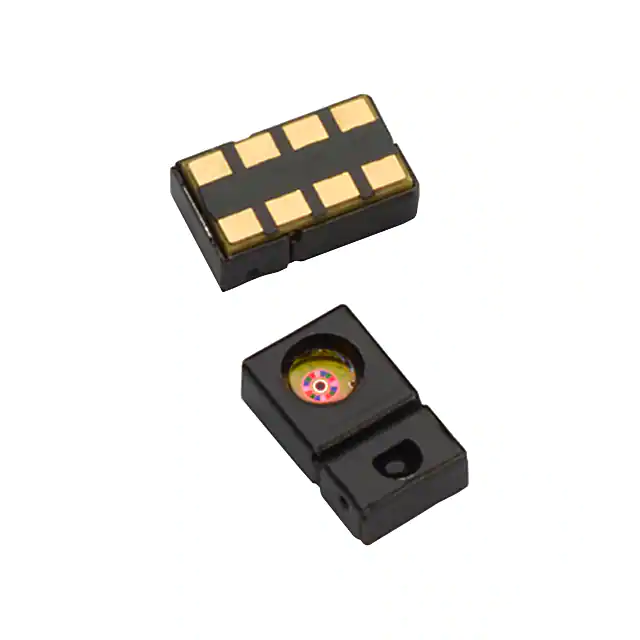
• Small Package L 3.94 × W 2.36 × H 1.35 mm
The color-sensing feature is useful in applications such as
LED RGB backlight control, solid-state lighting, reflected
LED color sampler, or fluorescent light color temperature
detection. The integrated IR blocking filter makes this
device an excellent ambient light sensor and color
temperature monitor sensor.
Ordering Information
Part Number
Packaging
Quantity
APDS-9950
Tape & Reel
5000 per reel
Applications
• OLED Display Control
• RGB LED Backlight Control
• Ambient Light Color Temperature Sensing
• Cell Phone Touch-screen Disable
• Automatic Speakerphone Enable
• Automatic Menu Pop-up
• Mechanical Switch Replacement
• Industrial Process Control
�Functional Block Diagram
VDD
LEDA
Regulated IR
LED Current Driver
Prox Control
Prox
Integration
LED K
Prox
ADC
Interrupt
Upper Limit
Prox
Data
SCL
Wait Control
RGBC Control
Clear
Red
Green
Blue
Clear ADC
Clear Data
Red ADC
Red Data
Upper Limit
I2C-bus Interface
Lower Limit
LDR
GND
INT
SDA
Lower Limit
Green ADC Green Data
Blue ADC
Blue Data
Description
The APDS-9950 is a next-generation digital color light
sensor device containing four integrating analog-todigital converters (ADCs) that integrate currents from
photodiodes. Multiple photodiode segments for red,
green, blue, and clear are geometrically arranged to
reduce the reading variance as a function of the incident
light angle. Integration of all color sensing channels occurs
simultaneously. Upon completion of the conversion cycle,
the conversion result is transferred to the corresponding
data registers. The transfers are double-buffered to
ensure that the integrity of the data is maintained.
Communication with the device is accomplished through
a fast (up to 400 kHz), two-wire I2C serial bus for easy
connection to a microcontroller or embedded controller.
The APDS-9950 provides a separate pin for level-style
interrupts. When interrupts are enabled and a preset
value is exceeded, the interrupt pin is asserted and
remains asserted until cleared by the controlling firmware.
The interrupt feature simplifies and improves system
efficiency by eliminating the need to poll a sensor for a
light intensity or proximity value. An interrupt is generated
when the value of a clear channel or proximity conversion
exceeds either an upper or lower threshold. In addition,
a programmable interrupt persistence feature allows
the user to determine how many consecutive exceeded
thresholds are necessary to trigger an interrupt. Interrupt
thresholds and persistence settings are configured
independently for both clear and proximity.
2
Proximity detection is done using a dedicated proximity
photodiode centrally located beneath an internal lens, an
internal LED, and a driver circuit. The driver circuit requires
no external components and is trimmed to provide a
calibrated proximity response. Customer calibrations are
usually not required.
The number of proximity LED pulses can be programmed
from 1 to 255 pulses. Each pulse has a 14 µs period.
This LED current coupled with the programmable number
of pulses provides a 2000:1 contiguous dynamic range.
�I/O Pins Configuration
Pin
Name
Type
Description
1
SDA
I/O
I2C serial data I/O terminal - serial data I/O for I2C-bus
2
INT
O
Interrupt - open drain (active low)
3
LDR
LED driver input for proximity IR LED, constant current source LED driver
4
LEDK
LED Cathode, connect to LDR pin when using internal LED driver circuit
5
LEDA
LED Anode, connect to VBATT on PCB
6
GND
Power supply ground. All voltages are referenced to GND
7
SCL
8
VDD
I
I2C serial clock input terminal - clock signal for I2C serial data
Power supply voltage
Absolute Maximum Ratings over operating free-air temperature range (unless otherwise noted)*
Parameter
Symbol
Power supply voltage [1]
VDD
Input voltage range
VIN
Output voltage range
Storage temperature range
Min
Max
Units
3.8
V
-0.5
3.8
V
VOUT
-0.3
3.8
V
Tstg
-40
85
°C
Conditions
* Stresses beyond those listed under “absolute maximum ratings” may cause permanent damage to the device. These are stress ratings only and
functional operation of the device at these or any other conditions beyond those indicated under “recommended operating conditions” is not
implied. Exposure to absolute-maximum-rated conditions for extended periods may affect device reliability.
Note 1. All voltages are with respect to GND.
Recommended Operating Conditions
Parameter
Symbol
Min
Operating ambient temperature
TA
Power supply voltage
VDD
Supply voltage accuracy, VDD total
error including transients
LED supply voltage
VBATT
Typ
Max
Units
-30
85
°C
2.5
3.5
V
-3
+3
%
2.5
4.5
V
Operating Characteristics, VDD = 3 V, TA = 25 °C (unless otherwise noted)
Parameter
Symbol
IDD supply current
IDD
Min
Typ
Max
Units
Test Conditions
235
330
µA
Active – LDR pulses off
85
2.5
Wait State
Sleep Mode – No I2C activity
10
VOL INT, SDA output low voltage
VOL
0
0.4
V
ILEAK leakage current, SDA, SCL, INT pins
ILEAK
−5
5
µA
ILEAK leakage current, LDR P\pin
ILEAK
−10
10
µA
SCL, SDA input high voltage, VIH
VIH
1.25
VDD
V
SCL, SDA input low voltage, VIL
VIL
0.54
V
3
3 mA sink current
�Optical Characteristics, VDD = 3 V, TA = 25 °C, AGAIN = 16×, AEN = 1 (unless otherwise noted) [1]
Parameter
Red Channel
Min
Irradiance
responsitivity
Typ
Green Channel
Max
Min
0%
15%
4%
75%
Typ
Blue Channel
Max
Min
10%
42%
25%
55%
110%
0%
Typ
Clear Channel
Max
Min
Typ
Max
60%
95%
14
17.5
21
85%
8%
45% 14.96
18.7
22.44
14%
3%
24%
20
24
16
Units
Test
Conditions
counts
/µW
/cm2
λD = 465 nm [2]
λD = 525 nm [3]
λD = 625 nm [4]
Notes:
1. The percentage shown represents the ratio of the respective red, green, or blue channel value to the clear channel value.
2. The 465 nm input irradiance is supplied by an InGaN light-emitting diode with the following characteristics:
dominant wavelength λD = 465 nm, spectral halfwidth Δλ½ = 22 nm.
3. The 525 nm input irradiance is supplied by an InGaN light-emitting diode with the following characteristics:
dominant wavelength λD = 525 nm, spectral halfwidth Δλ½ = 35 nm.
4. The 625 nm input irradiance is supplied by a AlInGaP light-emitting diode with the following characteristics:
dominant wavelength λD = 625 nm, spectral halfwidth Δλ½ = 15 nm.
RGBC Characteristics, VDD = 3 V, TA = 25 °C, AGAIN = 16×, AEN = 1 (unless otherwise noted)
Parameter
Min
Typ
Max
Units
Test Conditions
0
5
counts
Ee = 0, AGAIN = 60×,
ATIME = 0×D6 (100 ms)
2.4
2.56
ms
ATIME = 0×FF
256
steps
Full scale ADC counts per step
1023
counts
Full scale ADC count value
65535
counts
Dark ALS count value
ADC integration time step size
2.27
ADC number of integration steps
1
Gain scaling, relative to 1× gain
setting
ATIME = 0×C0 (153.6 ms)
3.6
4
4.4
4×
14.4
16
17.6
16×
54
60
66
60×
Proximity Characteristics, VDD = 3 V, TA = 25 °C, PEN = 1 (unless otherwise noted)
Parameter
Min
IDD supply current – LDR Pulse On
ADC conversion time step size
Typ
3
2.27
ADC number of integration steps
2.4
0
Units
2.56
ms
steps
1023
counts
255
pulses
LED pulse period
14.0
µs
LED pulse width – LED on time
6.3
µs
LED drive current
100
mA
Proximity ADC count value, no
object
Proximity ADC count value, 100
mm distance object
4
350
Test Conditions
mA
1
Full scale ADC counts
LED pulse count
Max
PDRIVE = 0
50
PDRIVE = 1
25
PDRIVE = 2
12.5
PDRIVE = 3
ISINK sink current
@ 0.6 V, LDR pin
125
250
counts
Dedicated power supply VBATT =
3 V LED driving 8 pulses, PDRIVE
= 00, PGAIN = 00, open view (no
glass) and no reflective object
above the module.
440
530
counts
Reflecting object – 73 mm ×
83 mm Kodak 90% grey card,
100 mm distance, LED driving 8
pulses, PDRIVE = 00, PGAIN = 00,
open view (no glass) above the
module.
�IR LED Characteristics, VDD = 3 V, TA = 25 °C (unless otherwise noted)
Parameter
Min
Typ
Max
Units
Test Conditions
Peak Wavelength, λP
850
nm
IF = 20 mA
Spectrum Width, Half Power, Δλ
40
nm
IF = 20 mA
Optical Rise Time, TR
20
ns
IF = 100 mA
Optical Fall Time, TF
20
ns
IF = 100 mA
Wait Characteristics, VDD = 3 V, TA = 25 °C, WEN = 1 (unless otherwise noted)
Parameter
Min
Typ
Max
Units
Test Conditions
Wait Step Size
2.27
2.4
2.56
ms
W TIME = 0×FF
AC Electrical Characteristics, VDD = 3 V, TA = 25 °C (unless otherwise noted) *
Parameter
Clock frequency (I2C-bus only)
Bus free time between a STOP and START condition
Symbol
Min.
Max.
Unit
fSCL
0
400
kHz
tBUF
1.3
–
µs
Hold time (repeated) START condition. After this period, the first clock pulse
is generated
tHDSTA
0.6
–
µs
Set-up time for a repeated START condition
tSU;STA
0.6
–
µs
Set-up time for STOP condition
tSU;STO
0.6
–
µs
Data hold time
tHD;DAT
0
–
ns
Data set-up time
tSU;DAT
100
–
ns
LOW period of the SCL clock
tLOW
1.3
–
µs
HIGH period of the SCL clock
tHIGH
0.6
–
µs
Clock/data fall time
tf
–
300
ns
Clock/data rise time
tr
–
300
ns
Input pin capacitance
Ci
–
10
pF
* Specified by design and characterization; not production tested.
t LOW
tr
V IH
V IL
SCL
t HD;STA
t HD;DAT
t BUF
t HIGH
t SU;STA
t SU;STO
tSU;DAT
V IH
V IL
SDA
P
Stop
Condition
S
Start
Condition
Figure 1. Timing Diagrams
5
tf
S
P
�20000
1
16000
0.8
Avg Sensor LUX
Normalized PD Responsitivity
1.2
R
Clear
0.6
G
0.4
4000
0.2
400
500
600 700 800
Wavelength (nm)
900
1000
0.4 0.5 0.6 0.7
Meter LUX
Figure 4. ALS Sensor LUX vs Meter LUX using White Light
0.1
0.2
0.3
0.8
0.9
1
1000
900
800
700
600
500
400
300
200
100
0
4000
8000
12000
Meter LUX
16000
20000
100 200 300 400 500 600 700 800 900 1000
Meter LUX
Figure 5. ALS Sensor LUX vs Meter LUX using Incandescent Light
0
1.4
1.3
Normalized IDD @ 25 °C
1
0.9
0.8
0.7
0.6
0.5
0.4
0.3
0.2
0.1
0
0
0
Figure 3. ALS Sensor LUX vs Meter LUX using White Light
Avg Sensor LUX
Avg Sensor LUX
1
0.9
0.8
0.7
0.6
0.5
0.4
0.3
0.2
0.1
0
0
1100
Figure 2. Normalized PD Spectral Response
Avg Sensor LUX
8000
B
0
300
1.2
1.1
1
0.9
0.8
0.7
0
0.1
0.2
0.3
0.4 0.5 0.6
Meter LUX
0.7
0.8
Figure 6. ALS Sensor LUX vs Meter LUX using Incandescent Light
6
12000
0.9
1
0.6
2.5
2.7
Figure 7. Normalized IDD vs. VDD
2.9
VDD (V)
3.1
3.3
3.5
�1.2
Normalized Responsitivity
Normalized IDD @ 3V
1.15
1.1
1.05
1
0.95
0.9
0.85
0.8
-60
-40
-20
0
20
40
Temperature (°C)
60
80
100
1.1
1
0.9
0.8
0.7
0.6
0.5
0.4
0.3
0.2
0.1
0
-20
0
Angle (Deg)
20
40
60
18% Kodak Gray Card
Opteka Black Card
90% Kodak Gray Card
1000
800
600
400
200
-60
-40
-20
0
Angle (Deg)
20
40
60
4Pulse, 100 mA, 1×
8Pulse, 100 mA, 1×
16Pulse, 100 mA, 1×
1000
800
600
400
200
0
0
20
40
60
80
100
Distance (mm)
0
0
20
40
60
80
100
Distance (mm)
120
Figure 11a. Proximity Distance Profile (8Pulse, 100 mA, 1×)
1200
Proximity Count
-40
1200
Figure 10. Normalized LED Angular Emitting Profile
120
Figure 11b. Proximity Distance Profile (18% Kodak Gray Card)
7
-60
Figure 9. Normalized ALS Response vs. Angular Displacement
Proximity Count
Normalized Responsitivity
Figure 8. Normalized IDD vs. Temperature
1.1
1
0.9
0.8
0.7
0.6
0.5
0.4
0.3
0.2
0.1
0
140
160
140 160
�Principles of Operation
System State Machine
RGBC Operation
The APDS-9950 provides control of RGBC, proximity
detection and power management functionality through
an internal state machine. After a power-on-reset, the
device is in the sleep mode. As soon as the PON bit is set,
the device will move to the start state. It will then continue
through the Prox, Wait and RGBC states. If these states are
enabled, the device will execute each function. If the PON
bit is set to a 0, the state machine will continue until all
conversions are completed and then go into a low power
sleep mode.
The RGBC engine contains RGBC gain control (AGAIN)
and four integrating analog-to-digital converters (ADC)
for the RGBC photodiodes. The RGBC integration time
(ATIME) affects both the resolution and the sensitivity of
the RGBC reading. Integration of all four channels occurs
simultaneously and upon completion of the conversion
cycle, the results are transferred to the color data registers.
This data is also referred to as channel count. The transfers
are double-buffered to ensure that invalid data is not
read during the transfer. After the transfer, the device
automatically moves to the next state in accordance with
the configured state machine.
Sleep
PON = 1
(rO×00:b0)
ATIME (r0×01),
AGAIN (r0×OF, b1:0)
2.4 ms to 700 ms 1×, 4×, 16×, 60× Gain
PON = 0
(rO×00:b0)
Start
RGBC Control
Prox
RGBC
Clear
Red
Wait
Green
Blue
Clear ADC
Clear Data
CDATAH(r0×15), CDATA(r0×14)
Red ADC
Red Data
RDATAH(r0×17), RDATA(r0×16)
Green ADC Green Data
GDATAH(r0×19), GDATA(r0×18)
Blue Data
BDATAH (r0×1B), BDATA(r0×1A)
Blue ADC
Figure 12. Simplified State Diagram
Note:
In this document, the nomenclature uses the bit field name in italics
followed by the register number and bit number to allow the user
to easily identify the register and bit that controls the function. For
example, the power on (PON) is in register 0, bit 0. This is represented
as PON (r0:b0).
Figure 13. RGBC Operation
The registers for programming the integration and wait
times are a 2’s complement values. The actual time can be
calculated as follows:
ATIME = 256 − Integration Time/2.4 ms
Inversely, the time can be calculated from the register
value as follows:
Integration Time = 2.4 ms v (256 − ATIME)
For example, if a 100 ms integration time is needed, the
device needs to be programmed to:
256 − (100 / 2.4) = 256 − 42 = 214 = 0×D6
Conversely, the programmed value of 0×C0 would
correspond to:
(256 − 0×C0) × 2.4 = 64 × 2.4 = 154 ms
8
�Proximity Detection
LEDA
IR
LED
PPULSE(r0×0E)
LEDK
LDR
Regulated IR
LED Current Driver
Prox Control
Prox
Integration
Object
Prox
ADC
PVALID(r0×13, b1)
Prox
Data
PDATAH(r0×019)
PDATAL(r0×018)
Prox Photodiode
Background Energy
Figure 14. Proximity Detection
Proximity detection measures IR signal energy reflected
off a remote object to determine its relative distance.
Figure 14 shows light rays emitting from the internal IR
LED, reflecting off an object, and being detected by the
proximity photodiode. The system response is managed
by controlling the number of IR pulses set in PPULSE
(Proximity Pulse Count Register).
The internal LED current driver provides a regulated
current sink on the LDR terminal that eliminates the need
for external components. If even higher LED output is
needed, currents can be switched using an external PFET,
gated by the LDR pin. The PFET can then sink current from
LEDK to ground with an appropriate external currentlimiting resistor.
Referring to the Expanded State Diagram (Figure 17), the
LED current driver pulses the internal IR LED during the
Prox Accum state. Using PPULSE, 1 to 255 proximity pulses
can be programmed. When deciding on the number of
proximity pulses, keep in mind that the signal increases
proportionally to PPULSE, while noise increases by the
square root of PPULSE.
To negate ambient light from the photodiode signal, the
background energy is subtracted from the total energy
received. Figure 15 illustrates the timing of the LED pulse.
The circuitry used to cancel the background energy
causes the pulse duty cycle to be asymmetrical as shown.
During the LED On time, the reflected signal and the
background energy are integrated by the sensor. During
the LED Off time, the background energy is subtracted
from the integrated value leaving the reflected IR signal to
accumulate from pulse to pulse.
9
After the programmed number of proximity pulses have
been generated, the proximity ADC converts and scales
the proximity measurement to a 16-bit value, then stores
the result in two 8-bit proximity data (PDATAx) registers.
The PSAT control (Control Register) can be used to assist
with detecting analog saturation at the sensor. When
PSAT = 1 the PDATA output registers will show the dark
current value (< 5) if saturation is determined to be likely.
When PSAT = 0 the PDATA registers will contain the ADC
output but if a saturation event happened the results will
be inaccurate.
Once the first proximity cycle has completed, the
proximity valid (PVALID) bit (Status Register) will be set
and remain set until the proximity detection function is
disabled (PEN).
Reflected IR LED +
Background Energy
Background
Energy
LED On
LED Off
6.3 s
14.0 s
IR LED Pulses
Figure 15. Proximity LED Current Driver Waveform
�Interrupts
The interrupt feature simplifies and improves system
efficiency by eliminating the need to poll the sensor for
light intensity or proximity values outside of a user-defined
range. While the interrupt function is always enabled and
it’s status is available in the status register (0×13), the
output of the interrupt state can be enabled using the
proximity interrupt enable (PIEN) or Clear interrupt enable
(AIEN) fields in the enable register (0×00).
Four 16-bit interrupt threshold registers allow the user
to set limits below and above a desired light level and
proximity range. An interrupt can be generated when the
Clear data (CDATA) falls outside of the desired light level
range, as determined by the values in the Clear interrupt
low threshold registers (AILTx) and Clear interrupt high
threshold registers (AIHTx). Likewise, an out-of-range
proximity interrupt can be generated when the proximity
data (PDATA) falls below the proximity interrupt low
threshold (PILTx) or exceeds the proximity interrupt high
threshold (PIHTx).
Prox
Integration
Prox
ADC
Note: The thresholds are evaluated in sequence, first
the low threshold, then the high threshold. As a result,
if the low threshold is set above the high threshold, the
high threshold is ignored and only the low threshold is
evaluated.
To further control when an interrupt occurs, the device
provides a persistence filter. The persistence filter allows
the user to specify the number of consecutive out-ofrange Clear or proximity occurrences before an interrupt
is generated. The persistence register (0×0C) allows
the user to set the Clear persistence (APERS) and the
proximity persistence (PPERS) values. See the persistence
register for details on the persistence filter values. Once
the persistence filter generates an interrupt, it will
continue until a special function interrupt clear command
is received (see command register).
PIHTH(r0×0B), PIHTL(r0×0A)
PPERS(r0×0C, b7:4)
Upper Limit
Prox Persistence
Prox
Data
Lower Limit
PILTH(r0×09), PILTL(r0×08)
AIHTH(r0×07), AIHTL(r0×06)
Prox
Upper Limit
Clear
ADC
Clear
Data
Lower Limit
Clear
AILTH(r0×05), AILTL(r0×04)
Figure 16. Programmable Interrupt
10
APERS(r0×0C, b3:0)
Clear Persistence
�State Diagram
Figure 17 shows a more detailed flow for the state
machine. The device starts in the sleep mode. The PON
bit is written to enable the device. A 2.4 ms delay will
occur before entering the start state. If the PEN bit is
set, the state machine will step through the proximity
states of proximity accumulate and then proximity ADC
conversion. As soon as the conversion is complete, the
state machine will move to the following state.
If the WEN bit is set, the state machine will then cycle
through the wait state. If the WLONG bit is set, the wait
cycles are extended by 12 over normal operation. When
the wait counter terminates, the state machine will step
to the RGBC state.
The AEN should always be set, even in proximity-only
operation. In this case, a minimum of 1 integration time
step should be programmed. The RGBC state machine
will continue until it reaches the terminal count, at which
point the data will be latched in the RGBC register and the
interrupt set, if enabled.
Sleep
!PON
I 2 C Start
Prox
PPULSE: 0 ~ 255 pulses
Time: 14.0 µs/pulse
Range: 0 ~ 3.6 ms
Time: 2.4 ms
PTIME: 1 ~ 256 steps
Time: 2.4 ms/step
Range: 2.4 ms ~ 614 ms
Prox
Accum
(Note 1)
RGBC
Idle
PEN
RGBC
ADC
Prox
Wait
Prox
ADC
!WEN &
!AEN
!AEN
(Note 3)
ATIME: 1 ~ 256 steps
Time: 2.4 ms/step
Range: 2.4 ms ~ 614 ms
!PEN & !WEN
& AEN
!PEN & WEN
& AEN
RGBC
Init
Time: 2.4 ms
!WEN &
AEN
AEN
WEN
Wait
WTIME: 1 ~ 256 steps
WLONG = 0
WLONG = 1
28.8 ms/step
Time: 2.4 ms/step
Range: 2.4 ms ~ 614 ms 28.8 ms ~ 7.37 s
Notes:
1. There is a 2.4 ms warm-up delay if PON is enabled. If PON is not enabled, the device will return to the Sleep state, as shown.
2. PON, PEN, WEN, AEN, and SAI are fields in the Enable register (0x00).
3. PON=1, PEN-1, WEN-1, AEN=0 is unsupported and will lead to erroneous proximity readings.
Figure 17. Expanded State Diagram
11
�I2C Protocol
The I2C standard provides for three types of bus
transaction: read, write, and a combined protocol. During
a write operation, the first byte written is a command byte
followed by data. In a combined protocol, the first byte
written is the command byte followed by reading a series
of bytes. If a read command is issued, the register address
from the previous command will be used for data access.
Likewise, if the MSB of the command is not set, the device
will write a series of bytes at the address stored in the last
valid command with a register address. The command
byte contains either control information or a 5-bit register
address. The control commands can also be used to clear
interrupts.
Interface and control are accomplished through an I2C
serial compatible interface (standard or fast mode) to
a set of registers that provide access to device control
functions and output data. The devices support the 7-bit
I2C addressing protocol.
The device supports a single slave address of 0×39 Hex
using 7-bit addressing protocol. (Contact factory for other
addressing options.)
A
Acknowledge (0)
N
Not Acknowledged (1)
P
Stop Condition
R
Read (1)
S
Start Condition
Sr
Repeated Start Condition
W
Write (0)
…
Continuation of protocol
Master-to-Slave
Slave-to-Master
The I2C bus protocol was developed by Philips (now NXP).
For a complete description of the I2C protocol, please
review the NXP I2C design specification at http://www.
i2c−bus.org/references/.
1
7
1
1
8
1
8
1
S
Slave Address
W
A
Command Code
A
Data
A
8
1
8
1
Data
A
Data
A
1
...
P
I2C Write Protocol
1
7
1
1
S
Slave Address
R
A
1
...
P
I2C Read Protocol
1
7
1
1
8
1
1
7
1
1
8
1
S
Slave Address
W
A
Command Code
A
Sr
Slave Address
R
A
Data
A
I2C Read Protocol - Combined Format
I2C Protocol
12
8
1
Data
A
1
...
P
�Register Set
The APDS-9950 is controlled and monitored by data registers and a command register accessed through the serial
interface. These registers provide for a variety of control functions and can be read to determine results of the ADC
conversions.
Address
Register Name
R/W
Register Function
Reset Value
−−
COMMAND
W
Specifies register address
0×00
0x00
ENABLE
R/W
Enable of states and interrupts
0×00
0x01
ATIME
R/W
RBGC time
0×FF
0x03
WTIME
R/W
Wait time
0×FF
0x04
AILTL
R/W
Clear interrupt low threshold low byte
0×00
0x05
AILTH
R/W
Clear interrupt low threshold high byte
0×00
0x06
AIHTL
R/W
Clear interrupt high threshold low byte
0×00
0x07
AIHTH
R/W
Clear interrupt high threshold high byte
0×00
0x08
PILTL
R/W
Proximity interrupt low threshold low byte
0×00
0x09
PILTH
R/W
Proximity interrupt low threshold hi byte
0×00
0x0A
PIHTL
R/W
Proximity interrupt hi threshold low byte
0×00
0x0B
PIHTH
R/W
Proximity interrupt hi threshold hi byte
0×00
0x0C
PERS
R/W
Interrupt persistence filters
0×00
0x0D
CONFIG
R/W
Configuration
0×00
0x0E
PPULSE
R/W
Proximity pulse count
0×00
0x0F
CONTROL
R/W
Gain control register
0×00
0x12
ID
R
Device ID
ID
0x13
STATUS
R
Device status
0×00
0x14
CDATAL
R
Clear ADC low data register
0×00
0x15
CDATAH
R
Clear ADC high data register
0×00
0x16
RDATAL
R
Red ADC low data register
0×00
0x17
RDATAH
R
Red ADC high data register
0×00
0x18
GDATAL
R
Green ADC low data register
0×00
0x19
GDATAH
R
Green ADC high data register
0×00
0x1A
BDATAL
R
Blue ADC low data register
0×00
0x1B
BDATAH
R
Blue ADC high data register
0×00
0x1C
PDATAL
R
Proximity ADC low data register
0×00
0x1D
PDATAH
R
Proximity ADC high data register
0×00
The mechanics of accessing a specific register depends on the specific protocol used. See the section on I2C protocols
on the previous pages. In general, the COMMAND register is written first to specify the specific control/status register
for following read/write operations.
13
�Command Register
The command registers specifies the address of the target register for future write and read operations.
7
6
5
4
3
TYPE
2
1
COMMAND
COMMAND
Field
Bits
Description
COMMAND
7
Select Command Register. Must write as 1 when addressing COMMAND register.
TYPE
6:5
Selects type of transaction to follow in subsequent data transfers:
0
ADD
Field Value
Integration Time
00
Repeated byte protocol transaction
01
Auto-Increment protocol transaction
10
Reserved — Do not use
11
Special function – See description below
--
Byte protocol will repeatedly read the same register with each data access.
Block protocol will provide auto-increment function to read successive bytes.
ADD
4:0
Address field/special function field. Depending on the transaction type, see above, this field either
specifies a special function command or selects the specific control-status-register for following write
or read transactions. The field values listed below apply only to special function commands:
Field Value
Read Value
00000
Normal — no action
00101
Proximity interrupt clear
00110
Clear interrupt clear
00111
Proximity and Clear interrupt clear
other
Reserved – Do not write
Clear / Proximity Interrupt Clear. Clears any pending Clear / Proximity interrupt. This special function
is self-clearing.
Enable Register (0×00)
The ENABLE register is used primarily to power the APDS-9950 device on and off, and enable functions and interrupts.
ENABLE
7
6
5
4
3
2
1
0
Address
Reserved
Reserved
PIEN
AIEN
WEN
PEN
AEN
PON
0×00
Field
Bits
Description
Reserved
7:6
Reserved. Write as 0.
PIEN
5
Proximity Interrupt Enable. When asserted, permits proximity interrupts to be generated.
AIEN
4
Ambient Light Sensing (ALS) Interrupt Enable. When asserted, permits ALS interrupts to be
generated.
WEN [1][2]
3
Wait Enable. This bit activates the wait feature. Writing a 1 activates the wait timer. Writing a 0
disables the wait timer.
PEN [1][2]
2
Proximity Enable. This bit activates the proximity function. Writing a 1 enables proximity. Writing a 0
disables proximity.
AEN [1][2]
1
RGBC Enable. This bit activates the RGBC function. Writing a 1 enables RGBC. Writing a 0 disables
RGBC.
PON
0
Power ON. This bit activates the internal oscillator to permit the timers and ADC channels to operate.
Writing a 1 activates the oscillator. Writing a 0 disables the oscillator. During reads and writes over the
I2C interface, this bit is temporarily overridden and the oscillator is enabled, independent of the state
of the PON.
Notes:
1 The PON bit must be set = 1 for these functions to operate.
2. WEN = 1, PEN = 1, AEN = 0 is unsupported and will lead to erroneous proximity readings.
14
�RGBC Time Register (0×01)
The RGBC timing register controls the internal integration time of the RGBC clear and IR channel in the ADCs in 2.4 ms
increments. Upon power up, the RGBC time register is set to 0xFF.
Field
Bits
ATIME
7:0
Description
VALUE
INTEG_CYCLES
TIME
MAX COUNT
0xFF
1
2.4 ms
1024
0xF6
10
24 ms
10240
0xD6
42
101 ms
43008
0xAD
64
154 ms
65535
0x00
256
614 ms
65535
Wait Time Register (0×03)
Wait time is set 2.4 ms increments unless the WLONG bit is asserted in which case the wait times are 12× longer. WTIME
is programmed as a 2’s complement number. Upon power up, the Wait time register is set to 0×FF.
Field
Bits
WTIME
7:0
Description
REGISTER VALUE
WAIT TIME
TIME (WLONG = 0)
TIME (WLONG = 1)
0xFF
1
2.4 ms
0.029 sec
0xAB
85
204 ms
2.45 sec
0x00
256
614 ms
7.4 sec
Note: The Proximity Wait Time Register should be configured before PEN and/or AEN is/are asserted.
Clear Interrupt Threshold Registers (0×04 − 0×07)
The Clear interrupt threshold registers provide the values to be used as the high and low trigger points for the
comparison function for interrupt generation. If the value generated by the clear channel crosses below the lower
threshold specified, or above the higher threshold, an interrupt is asserted on the interrupt pin.
Register
Address
Bits
Description
AILTL
0×04
7:0
Clear channel low threshold lower byte
AILTH
0×05
7:0
Clear channel low threshold upper byte
AIHTL
0×06
7:0
Clear channel high threshold lower byte
AIHTH
0×07
7:0
Clear channel high threshold upper byte
Proximity Interrupt Threshold Registers (0×08 − 0×0B)
The proximity interrupt threshold registers provide the values to be used as the high and low trigger points for the
comparison function for interrupt generation. If the value generated by proximity channel crosses below the lower
threshold specified, or above the higher threshold, an interrupt is asserted on the interrupt pin.
Register
Address
Bits
Description
PILTL
0x08
7:0
Proximity ADC channel low threshold lower byte
PILTH
0x09
7:0
Proximity ADC channel low threshold upper byte
PIHTL
0x0A
7:0
Proximity ADC channel high threshold lower byte
PIHTH
0x0B
7:0
Proximity ADC channel high threshold upper byte
15
�Persistence Register (0×0C)
The persistence register controls the filtering interrupt capabilities of the device. Configurable filtering is provided to
allow interrupts to be generated after each ADC integration cycle or if the ADC integration has produced a result that
is outside of the values specified by threshold register for some specified amount of time. Separate filtering is provided
for proximity and the clear channel.
7
6
PERS
5
4
3
2
PPERS
1
0
APERS
0×0C
Field
Bits
Description
PPERS
7:4
Proximity Interrupt persistence. Controls rate of proximity interrupt to the host
processor.
APERS
3:0
Field Value
Meaning Interrupt Persistence Function
0000
Every
Every proximity cycle generates an interrupt
0001
1
1 consecutive proximity values out of range
0010
2
2 consecutive proximity values out of range
…
…
…
1111
15
15 consecutive proximity values out of range
Clear Interrupt persistence. Controls rate of Clear interrupt to the host processor.
Field Value
Meaning Interrupt Persistence Function
0000
Every
Every RGBC cycle generates an interrupt
0001
1
1 consecutive clear channel values out of range
0010
2
2 consecutive clear channel values out of range
0011
3
3 consecutive clear channel values out of range
0100
5
5 consecutive clear channel values out of range
0101
10
10 consecutive clear channel values out of range
0110
15
15 consecutive clear channel values out of range
0111
20
20 consecutive clear channel values out of range
1000
25
25 consecutive clear channel values out of range
1001
30
30 consecutive clear channel values out of range
1010
35
35 consecutive clear channel values out of range
1011
40
40 consecutive clear channel values out of range
1100
45
45consecutive clear channel values out of range
1101
50
50 consecutive clear channel values out of range
1110
55
55 consecutive clear channel values out of range
1111
60
60 consecutive clear channel values out of range
Configuration Register (0×0D)
The configuration register sets the wait long time.
7
6
CONFIG
5
4
Reserved
3
2
1
0
WLONG
Reserved
0×0D
Field
Bits
Description
Reserved
7:2
Reserved. Write as 0.
WLONG
1
Wait Long. When asserted, the wait cycles are increased by a factor 12x from that
programmed in the WTIME register.
Reserved
0
Reserved. Write as 0.
16
�Proximity Pulse Count Register (0×0E)
The proximity pulse count register sets the number of proximity pulses that will be transmitted.
7
6
5
4
PPULSE
3
2
1
0
PPULSE
0×0E
Field
Bits
Description
PPULSE
7:0
Proximity Pulse Count. Specifies the number of proximity pulses to be generated.
Control Register (0×0F)
The Gain register provides eight bits of miscellaneous control to the analog block. These bits typically control functions
such as gain settings and/or diode selection.
7
6
5
4
CONTROL
PDRIVE
Field
Bits
Description
PDRIVE
7:6
LED Drive Strength
PDIODE
PGAIN
AGAIN
17
5:4
3:2
1:0
3
PDIODE
2
PGAIN
Field Value
LED Strength
00
100 mA
01
50 mA
10
25 mA
11
12.5 mA
Proximity Diode Select
Field Value
LED Strength
00
Reserved
01
Reserved
10
Proximity uses the IR Diode
11
Reserved
Proximity Gain Control
Field Value
LED Strength
00
1× Gain
01
Reserved
10
Reserved
11
Reserved
RGBC Gain Control
Field Value
RGBC Gain Value
00
1× Gain
01
4× Gain
10
16× Gain
11
60× Gain
1
0
AGAIN
0×0F
�ID Register (0×12)
The ID register provides the value for the part number. The ID is a read-only register.
7
6
5
4
ID
3
2
1
0
ID
0×12
Field
Bits
Description
ID
7:0
Part number identification
0×69 = APDS-9950
Status Register (0×13)
The Status Register provides the internal status of the device. This register is read-only.
STATUS
7
6
5
4
3
2
1
0
Reserved
Reserved
PINT
AINT
Reserved
Reserved
PVALID
AVALID
0×13
Field
Bits
Description
Reserved
7:6
Reserved.
PINT
5
Proximity Interrupt.
AINT
4
Clear Interrupt.
Reserved
3:2
Reserved.
PVALID
1
Proximity Valid. Indicates that a proximity cycle has completed since PEN was
asserted
AVALID
0
RGBC Valid. Indicates that a RGBC cycle has completed since AEN was asserted
RGBC DATA Register (0×14 − 0×1B)
Clear, red, green, and blue data is stored as 16-bit values. To ensure the data is read correctly, a two-byte read I2C
transaction should be used with a read word protocol bit set in the command register. With this operation, when the
lower byte register is read, the upper eight bits are stored into a shadow register, which is read by a subsequent read to
the upper byte. The upper register will read the correct value even if additional ADC integration cycles end between the
reading of the lower and upper registers.
Register
Address
Bits
Description
CDATAL
0×14
7:0
Clear data low byte
CDATAH
0×15
7:0
Clear data high byte
RDATAL
0×16
7:0
Red data low byte
RDATAH
0×17
7:0
Red data high byte
GDATAL
0×18
7:0
Green data low byte
GDATAH
0×19
7:0
Green data high byte
BDATAL
0×1A
7:0
Blue data low byte
BDATAH
0×1B
7:0
Blue data high byte
Proximity DATA Register (0×1C − 0×1D)
Proximity data is stored as a 16-bit value. To ensure the data is read correctly, a two byte read I2C transaction should be
utilized with a read word protocol bit set in the command register. With this operation, when the lower byte register is
read, the upper eight bits are stored into a shadow register, which is read by a subsequent read to the upper byte. The
upper register will read the correct value even if additional ADC integration cycles end between the reading of the lower
and upper registers.
Register
Address
Bits
Description
PDATAL
0×1C
7:0
Proximity data low byte
PDATAH
0×1D
7:0
Proximity data high byte
18
�Application Information Hardware
In a proximity sensing system, the included IR LED can be
pulsed by the APDS-9950 with more than 100 mA of rapidly
switching current, therefore, a few design considerations
must be kept in mind to get the best performance. The key
goal is to reduce the power supply noise coupled back into
the device during the LED pulses. If VBATT does not exceed
the maximum specified LDR pin voltage (including when
the battery is being recharged), LEDA can be directly tied
to VBATT for best proximity performance.
In many systems, there is a quiet analog supply and a noisy
digital supply. By connecting the quiet supply to the VDD
pin and the noisy supply to the LED, the key goal can be
meet. Place a 1 µF low-ESR decoupling capacitor as close
as possible to the VDD pin and another at the LED anode,
and a 22 µF capacitor at the output of the LED voltage
regulator to supply the 100 mA current surge.
V BUS
Voltage
Regulator
LEDK
V DD
LDR
1 µF
C*
GND
APDS-9950
RP
RP
R PI
INT
SCL
Voltage
Regulator
LEDA
SDA
1 µF
≥ 10 µF
* Cap Value Per Regulator Manufacturer Recommendation
Figure 18a. Circuit Implementation using Separate Power Supplies
V BUS
22 Ω
Voltage
Regulator
LEDK
V DD
LDR
1 µF
≥ 10 µF
GND
APDS-9950
RP
RP
R PI
INT
SCL
LEDA
SDA
1 µF
Figure 18b. Circuit Implementation using Single Power Supply
If operating from a single supply, use a 22 Ω resistor
in series with the VDD supply line and a 1 µF low ESR
capacitor to filter any power supply noise. The previous
capacitor placement considerations apply.
VBUS in the above figures refers to the I2C-bus voltage
which is either VDD or 1.8 V. Be sure to apply the specified
I2C-bus voltage shown in the Available Options table for
the specific device being used.
19
The I2C signals and the Interrupt are open-drain outputs
and require pull−up resistors. The pull-up resistor (RP)
value is a function of the I2C-bus speed, the I2C-bus
voltage, and the capacitive load. A 10 kΩ pull-up resistor
(RPI) can be used for the interrupt line.
�Package Outline Dimensions
8
7
2
2
7
6
3
3
6
5
4
4
5
1.35 ±0.1
2.36 ±0.2
3.94 ±0.2
0.05
0.58 ±0.05
1.18 ±0.05
1.34
0.20 ±0.05
Ø 0.90 ±0.05
0.25 (×6)
1
3.73 ±0.1
1
2.40 ±0.05
8
PINOUT
1 - SDA
2 - INT
3 - LDR
4 - LEDK
5 - LEDA
6 - GND
7 - SCL
8 - VDD
0.80
0.60±0.075
(x8)
2.10 ±0.1
PCB Pad Layout
Suggested PCB pad layout guidelines for the Dual Flat No-Lead surface mount package are shown below.
0.60
0.80
0.72 (×8)
0.25 (×6)
0.60
Note: All linear dimensions are in mm.
20
0.05
0.72 ±0.075
(x8)
Ø 1.50 ±0.05
�±0
.10
4 ±0.10
0.29 ±0.02
B0
Ø1
Unit Orientation
.05
A
8 ±0.10
2.70 ±0.10
8° Max
A0
Note: All linear dimensions are in mm.
Reel Dimensions
21
1.70 ±0.10
±0
A
5.50 ±0.05
12 +0.30
-0.10
4.30 ±0.10
Ø1
. 50
2 ±0.05
1.75 ±0.10
Tape Dimensions
K0
6° Max
�Moisture Proof Packaging
All APDS-9950 options are shipped in moisture proof package. Once opened, moisture absorption begins. This part is
compliant to JEDEC MSL 3.
Units in A Sealed
Mositure-Proof
Package
Package Is
Opened (Unsealed)
Environment
less than 30 deg C, and
less than 60% RH?
Yes
Package Is
Opened less
than 168 hours?
Yes
No Baking
Is Necessary
No
Perform Recommended
Baking Conditions
Baking Conditions
No
Recommended Storage Conditions
Package
Temperature
Time
Storage Temperature
10 °C to 30 °C
In Reel
60 °C
48 hours
Relative Humidity
below 60% RH
In Bulk
100 °C
4 hours
If the parts are not stored in dry conditions, they must be
baked before reflow to prevent damage to the parts.
Baking should only be done once.
22
Time from unsealing to soldering
After removal from the bag, the parts should be soldered
within 168 hours if stored at the recommended storage
conditions. If times longer than 168 hours are needed, the
parts must be stored in a dry box.
�Recommended Reflow Profile
MAX 260° C
R3
R4
TEMPERATURE (°C)
255
230
217
200
180
150
120
R2
60 sec to 120 sec
Above 217° C
R1
R5
80
25
0
P1
HEAT UP
Process Zone
Heat Up
Solder Paste Dry
50
100
150
P2
SOLDER PASTE DRY
Symbol
P1, R1
P2, R2
P3, R3
Solder Reflow
P3, R4
Cool Down
P4, R5
Time maintained above liquidus point , 217 °C
Peak Temperature
Time within 5 °C of actual Peak Temperature
Time 25 °C to Peak Temperature
200
P3
SOLDER
REFLOW
250
P4
COOL
DOWN
300
t-TIME
(SECONDS)
∆T
Maximum ∆T/∆time
or Duration
25 °C to 150 °C
150 °C to 200 °C
200 °C to 260 °C
260 °C to 200 °C
200 °C to 25 °C
> 217 °C
260 °C
> 255 °C
25 °C to 260 °C
3 °C/s
100 s to 180 s
3 °C/s
-6 °C/s
-6 °C/s
60 s to 120 s
–
20 s to 40 s
8 mins
The reflow profile is a straight-line representation of
a nominal temperature profile for a convective reflow
solder process. The temperature profile is divided into four
process zones, each with different ∆T/∆time temperature
change rates or duration. The ∆T/∆time rates or duration
are detailed in the above table. The temperatures are
measured at the component to printed circuit board
connections.
In process zone P1, the PC board and component pins
are heated to a temperature of 150 °C to activate the flux
in the solder paste. The temperature ramp up rate, R1, is
limited to 3 °C per second to allow for even heating of
both the PC board and component pins.
Process zone P2 should be of sufficient time duration (100
to 180 seconds) to dry the solder paste. The temperature is
raised to a level just below the liquidus point of the solder.
Process zone P3 is the solder reflow zone. In zone P3, the
temperature is quickly raised above the liquidus point
For product information and a complete list of distributors, please go to our web site:
of solder to 260 °C (500 °F) for optimum results. The
dwell time above the liquidus point of solder should be
between 60 and 120 seconds. This is to assure proper
coalescing of the solder paste into liquid solder and
the formation of good solder connections. Beyond the
recommended dwell time the intermetallic growth within
the solder connections becomes excessive, resulting in
the formation of weak and unreliable connections. The
temperature is then rapidly reduced to a point below
the solidus temperature of the solder to allow the solder
within the connections to freeze solid.
Process zone P4 is the cool down after solder freeze. The
cool down rate, R5, from the liquidus point of the solder to
25 °C (77 °F) should not exceed 6 °C per second maximum.
This limitation is necessary to allow the PC board and
component pins to change dimensions evenly, putting
minimal stresses on the component.
It is recommended to perform reflow soldering no more
than twice.
www.avagotech.com
Avago Technologies, and the A logo are trademarks of Avago Technologies in the United States and other countries.
Data subject to change. Copyright © 2005-2015 Avago Technologies. All rights reserved.
AV02-3959EN - November 13, 2015
�