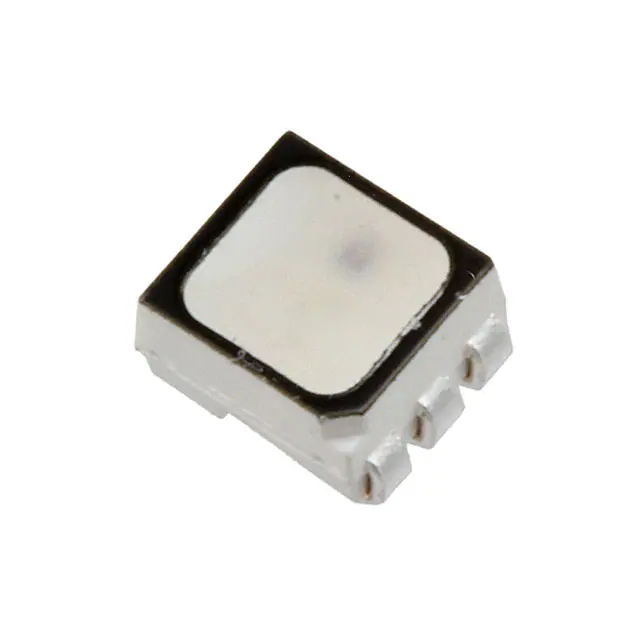
ASMT-YTB7-0AA02
Tricolor PLCC6 Black Surface Mount LED
Data Sheet
Description
Features
This family of SMT LEDs packaged in the form of PLCC-6
with separate heat path for each LED dice, enabling it to
be driven at higher current.
Standard PLCC-6 package (Plastic Leaded Chip Carrier)
with individual addressable pin-out for higher flexibility
of driving configuration
For easy pick & place, the LEDs are shipped in EIA-compliant tape and reel. Every reel is shipped from a single intensity and color bin; except red color for better uniformity.
LED package with diffused silicone encapsulation
These LEDs are compatible with reflow soldering process.
Compatible with reflow soldering process
This super wide viewing angle at 120° together with the
built in reflector pushing up the intensity of the light output makes these LED suitable to be used in the interior
electronics signs.
JEDEC MSL 3
The black top surface of the LED provides better contrast
enhancement especially in the full color sign application.
Using AlInGaP and InGaN dice technologies
Wide viewing angle at 120°
Water-Resistance (IPX6*) per IEC 60529:2001
•
The test is conducted on component level by mounting
the components on PCB with proper potting to protect
the leads. It is strongly recommended that customers
perform necessary tests on the components for their final
application
Applications
Indoor and outdoor full color display
CAUTION: These LEDs are Class 1C ESD sensitive. Please observe appropriate precautions during
handling and processing. Please refer to Avago Application Note AN-1142 for additional details.
CAUTION: Customer is advised to keep the LED in the MBB when not in use as prolonged exposure to
environment might cause the silver plated leads to tarnish, which might cause difficulties in soldering.
�Package Dimensions
Lead Configuration
4
3
5
2
1
0.50
6
2.30
2.30
2.80
2.30
3.00
1
Cathode
Blue
2
Cathode
Green
3
Cathode
Red
4
Anode
Red
5
Anode
Green
6
Anode
Blue
Notes:
1. All Dimensions are in millimeters
2. Tolerance = ±0.2 mm unless otherwise specified
3. Terminal Finish: Ag plating
4. Encapsulantion material: silicone resin
3.40
4
3
1.80
Red
5
2
Green
6
0.20
1
Blue
0.90
Table 1. Device Selection Guide
Color 1 - Red
Min. Iv
@20mA
Part Number
ASMT-YTB7-0AA02
Color 2 - Green
Typ. Iv Max Iv
@20mA @ 20mA
Min. Iv
@ 20mA
Color 3 - Blue
Typ. Iv Max Iv
@ 20mA @ 20mA
Min. Iv
@ 20mA
Typ. Iv Max Iv
@ 20mA @ 20mA
Bin ID
(mcd)
(mcd)
(mcd)
Bin ID
(mcd)
(mcd)
(mcd)
Bin ID
(mcd)
(mcd)
(mcd)
U2
560
650
1125
W2
1400
1900
2850
T1
285
384
560
Notes:
1. The luminous intensity IV, is measured at the mechanical axis of the LED package and it is tested in pulsing condition. The actual peak of the spatial
radiation pattern may not be aligned with this axis.
2. Tolerance = ± 12 %
Part Numbering System
ASMT – Y T B7 – 0 X 2 X 3 X 4 X 5
Packaging Option
2: 20mA testing current
Color Bin Selection
0: Red (Full distribution) Green (A,B,C), Blue (A,B,C,D)
Number of half intensity bin
A: 3half intensity bin
Min Intensity Bin
A: Red U2 / Green W2/ Blue T1
Package Type
B: Black Surface Tricolor
Color
T: Tricolor
Product Family
Y: Silicon Based PLCC6
2
�Table 2. Absolute Maximum Ratings (TA = 25°C)
Parameter
Red
Green & Blue
Unit
50
25
mA
100
100
mA
90
mW
DC forward current [1]
Peak forward current [2]
Power dissipation
125
Maximum junction temperature Tj max
Operating temperature range
110
°C
- 40 to + 100 [3]
°C
- 40 to + 100
°C
Storage temperature range
Note:
1. Derate linearly as shown in Figure 4a & 4b
2. Duty Factor = 10% Frequency = 1KHz
3. Refer to Figure 4a and Figure 4b for more information
Table 3. Optical Characteristics (TA = 25°C)
Luminous Intensity,
Iv, mcd [1]
Color
Min
Dominant Wavelength,
d (nm) [2]
Peak
Wavelength,
p (nm)
Viewing Angle
2½ (°) [3]
Typ
Max.
Min
Typ
Max
Typ.
Typ
Test Current
(mA)
Red
560
650
1125
617
623
627
630
120
20
Green
1400
1900
2850
525
529
537
522
120
20
Blue
285
384
560
465
469
475
465
120
20
Notes:
1. The luminous intensity Iv is measured at the mechanical axis of LED package and it is tested in pulsing condition. The actual peak of the spatial
radiation pattern may not be aligned with the axis.
2. The dominant wavelength is derived from the CIE Chromaticity Diagram and represents the perceived color of the device.
3. ½ is the off axis angle where the luminous intensity is ½ the peak intensity
Table 4. Electrical Characteristics (TA = 25°C)
Forward Voltage,
VF (V) [1]
Reverse Voltage
VR @100μA [3]
Reverse Voltage
VR @10μA [3]
Min
Thermal Resistance
RθJ-P (°C/W) [2]
Test Current
Typ
(mA)
Color
Min
Typ.
Max.
Min
Red
1.80
2.10
2.50
4
-
280
20
Green
2.80
3.10
3.60
-
4
240
20
Blue
2.80
3.10
3.60
-
4
240
20
Note:
1. Tolerance ± 0.1V.
2. One chip on thermal resistance
3. Indicated product final testing condition, long term reverse bias is not recommended.
3
�100
0.8
80
BLUE
GREEN
FORWARD CURRENT - mA
RELATIVE INTENSITY
1.0
RED
0.6
0.4
0.2
0.0
400
60
40
20
0
450
500
550
600
WAVELENGTH - nm
650
700
Figure 1. Relative Intensity vs Wavelength
0
1
2
3
FORWARD VOLTAGE - V
4
5
Figure 2. Forward Current –mA vs Forward Voltage
3.0
GREEN
BLUE
RED
NORMALIZED INTENSITY
2.5
2.0
1.5
1.0
0.5
0.0
0
10
20
30
FORWARD CURRENT - mA
Figure 3. Relative Intensity vs Forward Current
40
50
60
MAXIMUM FORWARD CURRRENT - mA
MAX ALLOWABLE CURRENT - mA
60
50 AlInGaP
40
30
InGaN
20
10
0
0
20
40
60
80
AMBIENT TEMPERATURE (°C)
100
120
Figure 4a. Maximum forward current vs. ambient temperature. (3 chips)
4
AlInGaP
50
40
30
InGaN
20
10
0
0
20
40
60
80
AMBIENT TEMPERATURE (°C)
100
120
Figure 4b. Maximum forward current vs. ambient temperature. (single chip)
�1.0
0.8
0.8
NORMALIZED INTENSITY
NORMALIZED INTENSITY
1.0
0.6
0.4
Red
Green
Blue
0.2
0.0
-90
-60
-30
0
30
60
ANGULAR DISPLACEMENT-DEGREE
0.4
Red
Green
Blue
0.2
0.0
90
Figure 5a. Radiation Pattern for X axis
0.6
-90
-60
-30
0
30
60
ANGULAR DISPLACEMENT-DEGREE
90
Figure 5b. Radiation Pattern for Y axis
Y
X
X
Y
Figure 5c. Component Axis for Radiation Patterns
0.5
Blue
Green
Red
1
0.1
-40
-20
0
20
40
60
80
TJ - JUNCTION TEMPERATURE
Figure 6. Relative Intensity vs Junction Temperature
5
FORWARD VOLTAGE SHIFT - V
NORMALZIED INTENSITY
10
100
120
Blue
Green
Red
0.4
0.3
0.2
0.1
0
-0.1
-0.2
-0.3
-40
-20
0
20
40
60
80
TJ - JUNCTION TEMPERATURE
Figure 7. Forward Voltage vs Junction Temperature
100
120
�1.35
4.35
4.35
4.35
1.60
0.40
0.50
Reflow
soldering
direction
5.25
0.50
0.40
2.35
4.35
1.60
Figure 8a. Recommended soldering land pattern.
Figure 8b. LED Configuration on land pattern
ID
OD
ID = 1.7mm
OD = 3.5mm
Figure 9. Recommended Pick and Place Nozzle Tip
10 to 30 SEC.
240°C MAX.
3°C/SEC. MAX.
183°C
100-150°C
-6°C/SEC.
MAX.
3°C/SEC.
MAX.
120 SEC. MAX.
60-150 SEC.
TIME
Figure 10. Recommended leaded reflow soldering profile.
TEMPERATURE
TEMPERATURE
20 SEC. MAX.
217°C
200°C
255 - 260 °C
3°C/SEC. MAX.
6°C/SEC. MAX.
150°C
3 °C/SEC. MAX.
100 SEC. MAX.
60 - 120 SEC.
TIME
Figure 11. Recommended Pb-free reflow soldering profile.
Note: For detail information on reflow soldering of Avago surface mount LEDs, do refer to Avago Application Note AN 1060 Surface Mounting SMT
LED Indicator Components
6
�Package
Marking
4.00 ±0.10
2.00 ±0.05
4.00 ±0.10
1.50 +0.10
–0
1.75 ±0.10
2.29 ±0.1
3.50 ±0.05
8.00 +0.30
–0.10
3.81 ±0.10
1.00 +0.10
–0
3.05 ±0.10
0.229 ±0.01
8°
Figure 12. Carrier tape Dimension
Ø 20.5 ±0.3
+0.5
2 –0
62.5 +0
–2.5
180
Ø 13 ±0.2
8.4 +1.50
–0.00 (MEASURED AT OUTER EDGE)
14.4 (MAX. MEASURED AT HUB)
LABEL AREA (111 mm x 57 mm)
WITH DEPRESSION (0.25 mm)
7.9 (MIN.)
10.9 (MAX.)
Figure 13. Reel Dimension
USER FEED DIRECTION
PIN 1
PRINTED LABEL
Figure 14. Reeling Orientation
7
�Packaging Label:
(i) Avago Mother Label (Available on MBB bags)
(1T) Lot: Lot Number
STANDARD LABEL LS0002
RoHS Compliant Halogen Free
e4 Max Temp
260C MSL3
(Q) QTY: Quantity
LPN:
CAT: Intensity Bin
(9D) MFG Date: Manufacturing Date
BIN: Color Bin
(1P) Item: Part Number
(P) Customer Item:
(V) Vendor ID:
(9D) Date Code: Date Code
DeptID:
Made In: Country of Origin
(ii) Avago Baby Label (Available on reel)
(1P) PART #: Part Number
(1T) LOT #: Lot Number
BABY LABEL COSB
(9D)MFG DATE: Manufacturing Date
QUANTITY: Packing Quantity
C/O: Country of Origin
(9D): DATE CODE:
(1T) TAPE DATE:
D/C: Date Code
001B V0.0
VF:
CAT: INTENSITY BIN
BIN: COLOR BIN
Example indicates luminous Intensity information for
Red, Green and Blue respectively from label:
BIN: A B
CAT: U2 W2 T1
Intensity for Blue
Color Bin for Blue
Intensity for Green
Color Bin for Green
Intensity for Red
8
Example indicates color bin information for Green and
Blue from label:
�Intensity Bin Select (X2, X3)
Color Bin Limit
Individual reel will contain parts from 1 half bin only
Red Color Bin Table
Min Iv Bin (Minimum Intensity Bin)
X2
Red
Green
Blue
A
U2
W2
T1
Bin
ID
Dominant
Wavelength
Min
Full
617.0
range
Number of Intensity bin from X2
Max
Chromaticity Coordinate
627.0
x
0.6850 0.6815 0.7000 0.7037
y
0.3149 0.3150 0.2966 0.2962
X3
Red
Green
Blue
Tolerance of each bin limit is ± 1 nm
A
3
3
3
Green Color Bin Table
Color Bin Select (X4)
Bin Min
ID Dom
Max
Dom
Individual Reel will contain part from 1 full bin only
A
531.0
525.0
Color Bin Combinations
X4
Red
Green
Blue
0
Full distribution
A,B,C
A,B,C,D
Intensity Bin Limits
B
528.0
534.0
C
531.0
537.0
Chromaticity Coordinate
x
0.1142
0.1624
0.2001
0.1625
y
0.8262
0.7178
0.6983
0.8012
x
0.1387
0.1815
0.2179
0.1854
y
0.8148
0.7089
0.6870
0.7867
x
0.1625
0.2001
0.2353
0.2077
y
0.8012
0.6983
0.6747
0.7711
Tolerance of each bin limit is ± 1 nm
Bin ID
Min (mcd)
Max (mcd)
U2
560.0
715.0
V1
715.0
900.0
V2
900.0
1125.0
W1
1125.0
1400.0
W2
1400.0
1800.0
X1
1800.0
2240.0
X2
2240
2850
Tolerance of each bin limit ± 12%
Blue Color Bin Table
Bin Min
ID Dom
Max
Dom
Chromaticity Coordinate
A
465.0
469.0
x
0.1355
0.1751
0.168
0.127
y
0.0399
0.0986
0.1094
0.053
B
467.0
471.0
x
0.1314
0.1718
0.1638
0.122
y
0.0459
0.1034
0.1167
0.063
x
0.1267
0.168
0.1593
0.116
y
0.0534
0.1094
0.1255
0.074
x
0.1215
0.1638
0.1543
0.1096
y
0.0626
0.1167
0.1361
0.0868
C
469.0
473.0
D
471.0
475.0
Tolerance f each bin limit is ± 1 nm
9
�Handling Precaution
The encapsulation material of the LED is made of silicone
for better product reliability. Since silicone is a soft material, avoid pressing on the silicon or poking the silicon
with a sharp object as the product could be damaged
and cause premature failure. During assembly handling,
the unit should be held by the body only. Please refer to
Avago Application Note AN 5288 for additional handling
information and proper procedures.
Moisture Sensitivity
This product has a Moisture Sensitive Level 3 rating
per JEDEC J-STD-020. Refer to Avago Application Note
AN5305, Handling of Moisture Sensitive Surface Mount
Devices, for additional details and a review of proper handling procedures.
A. Storage before use
- An Unopened moisture barrier bag (MBB) can be
stored at
很抱歉,暂时无法提供与“ASMT-YTB7-0AA02”相匹配的价格&库存,您可以联系我们找货
免费人工找货- 国内价格
- 1+6.05000
- 100+5.04900
- 1000+4.58700
- 2000+4.40000
- 国内价格
- 50+6.64820
- 125+6.48158
- 250+6.31912
- 500+6.16187