ASSR-4110, ASSR-4111, ASSR-4120
and ASSR-4130 (Preliminary Product Release)
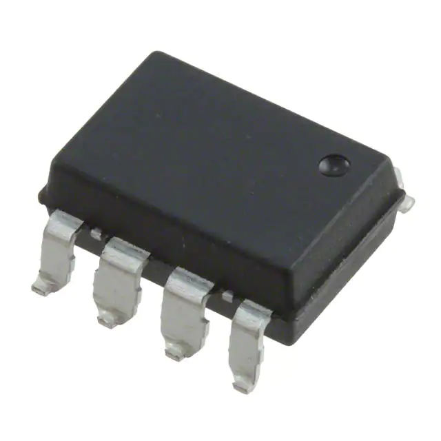
General Purpose, Form A, Solid State Relay (Photo MOSFET)
(400V/0.12A/25Ω)
Data Sheet
Lead (Pb) Free
RoHS 6 fully
compliant
RoHS 6 fully compliant options available;
-xxxE denotes a lead-free product
Description
Features
The ASSR-41xx Series consists of an AlGaAs infrared
light-emitting diode (LED) input stage optically
coupled to a high-voltage output detector circuit. The
detector consists of a high-speed photovoltaic diode
array and driver circuitry to switch on/off two discrete
high voltage MOSFETs. The relay turns on (contact
closes) with a minimum input current of 3mA through
the input LED. The relay turns off (contact opens) with
an input voltage of 0.8V or less.
• Compact Solid-State Bi-directional Signal Switch
The single channel configurations, ASSR-4110 and
ASSR-4111, are equivalent to 1 Form A Electromechanical Relays (EMR), and the dual channel configuration,
ASSR-4120 and ASSR-4130, are equivalent to 2 Form
A EMR. They are available in 4-pin SO, 6-pin DIP, 8-pin
DIP and Gull Wing Surface Mount for DIP packages
and true surface mount SO-8 pin. Their electrical and
switching characteristics are specified over the temperature range of -40°C to +85°C. They are used for
general purpose switching of signals and low power
AC/DC loads.
• Low On-Resistance:
5.5Ω Typical for DC-only, 16Ω Typical for AC/DC
ASSR-4111 enables AC/DC and DC-only output connec
tions. For DC-only connection, the output current, Io,
increases to 0.24A and the on-resistance, R(ON) reduces
to 8.5Ω.
• Single and Dual Channel Normally-off Single-PoleSingle-Throw (SPST) Relay
• 400V Output Withstand Voltage
• 0.12A or 0.24A Current Rating
(See Schematic for ASSR-4111 Connection A and B)
• Low Input Current: CMOS Compatibility
• Very High Output Off-state Impedance:
10 Teraohms Typical
• High Speed Switching:
0.1ms (Ton), 0.02ms (Toff ) Typical
• High Transient Immunity: >1kV/µs
• High Input-to-Output Insulation Voltage
(Safety and Regulatory Approvals)
- 3750 Vrms for 1 min per UL1577
- CSA Component Acceptance
Applications
• ���������������������������
Telecommunication Switching
Functional Diagram
• �������������������
Data Communications
Opto-isolation
• �������������������
Industrial Controls
• �������
Medical
1
4
Turn-off
Circuit
2
3
Truth Table
• ��������
Security
LED
Output
Off
Open
• ����������������������������
EMR / Reed Relay Replacement
On
Close
Single Channel, SPST Relay,
1 Form A in 4-Pin SO Package
CAUTION: It is advised that normal static precautions be taken in handling and assembly
of this component to prevent damage and/or degradation which may be induced by ESD.
�Ordering Information
ASSR-xxxx is UL Recognized with 3750 Vrms for 1 minute per UL1577 and is approved under CSA Component Acceptance Notice #5, File CA 88324.
Option
Part number
RoHS Compliant
-003E
ASSR-4110
-503E
-001E
ASSR-4111
-301E
-501E
-002E
ASSR-4120
-302E
-502E
ASSR-4130
(Preliminary Product
Release)
-005E
-505E
Package
SO-4
300mil
DIP-6
300 mil
DIP-8
SO-8
Surface
Mount
Gull
Wing
Tape
& Reel
X
Quantity
100 units per tube
X
X
1500 units per reel
50 units per tube
X
X
X
X
50 units per tube
X
1000 units per reel
50 units per tube
X
X
X
X
50 units per tube
X
X
1000 units per reel
50 units per tube
X
X
1000 units per reel
To order see attached table, choose a part number from the part number column and combine with the desired
option from the option column to form an order entry.
Example 1:
ASSR-4111-501E to order product of 300mil DIP-6 Gull Wing Surface Mount package in Tape and Reel packaging
and RoHS Compliant.
Example 2:
ASSR-4120-002E to order product of 300mil DIP-8 package in tube packaging and RoHS Compliant.
Option datasheets are available. Contact your Avago sales representative or authorized distributor for information.
Schematic
ASSR-4110
Opto-isolation
1
Opto-isolation
4
�
4
2
3
Equivalent
Relay
Diagram
Turn-off
Circuit
2
1
3
�ASSR-4111 Connection A
Opto -isolation
Turn-off
Circuit
2
Opto -isolation
6
1
Equivalent
Relay
Diagram
5
Vo
1
6
2
4
4
3
ASSR-4111 Connection B
Opto -isolation
Opto -isolation
1
6
+
Vo
5
Turn-off
Circuit
2
-
Equivalent
Relay
Diagram
1
4 and 6
2
5
3
4
ASSR-4120 and ASSR-4130
Opto-isolation
Opto-isolation
1
8
Turn-off
Circuit
2
7
3
6
Turn-off
Circuit
4
�
5
Equivalent
Relay
Diagram
1
8
2
7
3
6
4
5
�Package Outline Drawings
ASSR-4110 4-Pin Small Outline Package
LAND PATTERN RECOMMENDATION
2.54
(0.100)
0.80
(0.031)
LEAD FREE
TYPE NUMBER
DATE CODE
1.20
(0.047)
xxxx
4.40±0.20
(0.173±0.008)
YWW
0.375
(0.015)
4.80
(0.189)
6.8±0.4
(0.268±0.016)
2.540
(0.10)
0.41
(0.016)
4.3±0.2
(0.169±0.008)
2.0±0.2
(0.079±0.009)
0.46
(0.018)
0.20
(0.008)
DIMENSIONS IN MILLIMETERS AND (INCHES)
OPTION NUMBER 500 AND UL RECOGNITION NOT MARKED
0.5
(0.02)
0.102±0.102
(0.004±0.004)
ASSR-4111 6-Pin DIP Package
7.36 (0.290)
7.88 (0.310)
9.40 (0.370)
9.90 (0.390)
6
5
4
LEAD FREE
PIN
ONE
DOT
1
2
RU
UL
RECOGNITION
6.10 (0.240)
6.60 (0.260)
4.70 (0.185) MAX.
(0.020)
(0.040)
2.66 (0.105) MIN.
0.45 (0.018)
0.65 (0.025)
2.28 (0.090)
2.80 (0.110)
DIMENSIONS IN MILLIMETERS AND (INCHES).
�
5¡ TYP.
3
1.78 (0.070) MAX.
2.16 (0.085)
2.54 (0.100)
0.20 (0.008)
0.33 (0.013)
DATE CODE
A XXXX
YYWW
TYPE
NUMBER
0.5
(0.02)
�ASSR-4111 6-Pin DIP Package with Gull Wing Surface Mount Option 300
9.65 ± 0.25
(0.380 ± 0.010)
LAND PATTERN RECOMMENDATION
6.35 ± 0.25
(0.250 ± 0.010)
10.9 (0.430)
1.27 (0.050)
2.0 (0.080)
9.65 ± 0.25
(0.380 ± 0.010)
1.78
(0.070)
MAX.
0.635 ± 0.130
(0.025 ± 0.005)
7.62 ± 0.25
(0.300 ± 0.010)
4.19
MAX.
(0.165)
0.635 ± 0.25
(0.025 ± 0.010)
2.54
(0.100)
TYP.
2.29
(0.090)
0.20 (0.008)
0.30 (0.013)
12¡ NOM.
NOTE: FLOATING LEAD PROTRUSION IS 0.25 mm (10 mils) MAX.
ASSR-4120 8-Pin DIP Package
7.62 ± 0.25
(0.300 ± 0.010)
9.65 ± 0.25
(0.380 ± 0.010)
TYPE NUMBER
8
7
6
5
YYWW RU
1
1.19 (0.047) MAX.
6.35 ± 0.25
(0.250 ± 0.010)
DATE CODE
A XXXX
LEAD FREE
OPTION CODE*
2
3
4
UL
RECOGNITION
1.78 (0.070) MAX.
5° TYP.
3.56 ± 0.13
(0.140 ± 0.005)
4.70 (0.185) MAX.
+ 0.076
0.254 - 0.051
+ 0.003)
(0.010 - 0.002)
0.51 (0.020) MIN.
2.92 (0.115) MIN.
1.080 ± 0.320
(0.043 ± 0.013)
�
0.65 (0.025) MAX.
2.54 ± 0.25
(0.100 ± 0.010)
DIMENSIONS IN MILLIMETERS AND (INCHES).
OPTION NUMBERS 300 AND 500 NOT MARKED.
�ASSR-4120 8-Pin DIP Package with Gull Wing Surface Mount Option 300
LAND PATTERN RECOMMENDATION
9.65 ± 0.25
(0.380 ± 0.010)
7
8
6
1.016 (0.040)
5
6.350 ± 0.25
(0.250 ± 0.010)
1
2
3
10.9 (0.430)
4
2.0 (0.080)
1.27 (0.050)
9.65 ± 0.25
(0.380 ± 0.010)
1.780
(0.070)
MAX.
1.19
(0.047)
MAX.
7.62 ± 0.25
(0.300 ± 0.010)
3.56 ± 0.13
(0.140 ± 0.005)
1.080 ± 0.320
(0.043 ± 0.013)
0.635 ± 0.25
(0.025 ± 0.010)
0.635 ± 0.130
2.54
(0.025 ± 0.005)
(0.100)
BSC
DIMENSIONS IN MILLIMETERS (INCHES).
LEAD COPLANARITY = 0.10 mm (0.004 INCHES).
+ 0.076
0.254 - 0.051
+ 0.003)
(0.010 - 0.002)
12° NOM.
NOTE: FLOATING LEAD PROTRUSION IS 0.25 mm (10 mils) MAX.
ASSR-4130 8-Pin Surface Mount DIP Package (Preliminary Product Release)
LAND PATTERN RECOMMENDATION
2.54
(0.100)
TYPE NUMBER
DATE CODE
1.20
(0.047)
LEAD FREE
4.40±0.20
(0.173±0.008)
A XXXX
YYWW
0.80
(0.031)
6.81±0.40
(0.268±0.016)
4.80
(0.189)
0.41
(0.016)
2.54
(0.100)
9.4±0.2
(0.369±0.008)
DIMENSIONS IN MILLIMETERS AND (INCHES)
�
0.20
(0.008)
051
(0.020)
2±0.2
(0.079±0.008)
0.102±0.102
(0.004±0.004)
0.46
(0.018)
�Lead Free IR Profile
tp
TEMPERATURE (°C)
Tp
TL
260 +0/-5°C
TIME WITHIN 5°C of ACTUAL
PEAK TEMPERATURE
20-40 SEC.
217°C
RAMP-UP
3°C/SEC. MAX.
150 - 200°C
T smax
RAMP-DOWN
6°C/SEC. MAX.
T smin
ts
PREHEAT
60 to 180 SEC.
tL
60 to 150 SEC.
25
t 25°C to PEAK
TIME (SECONDS)
NOTES:
THE TIME FROM 25°C to PEAK TEMPERATURE = 8 MINUTES MAX.
Tsmax = 200°C, Tsmin = 150°C
Non-halide flux should be used.
Regulatory Information
The ASSR-4110, ASSR-4111, ASSR-4120 and ASSR-4130 (Preliminary Product Release) are approved by the following
organizations:
UL
Approvals under UL 1577, component recognition program up to VISO = 3750 VRMS
Approvals under CSA Component Acceptance Notice #5.
Insulation and Safety Related Specifications
Parameter
Symbol
ASSR4110
ASSR-4111
ASSR-4120
ASSR4130
Units
Conditions
Minimum External Air
Gap (Clearance)
L(101)
4.9
7.1
4.9
mm
Measured from input terminals to output
terminals, shortest distance through air.
Minimum External Tracking (Creepage)
L(102)
4.9
7.4
4.8
mm
Measured from input terminals to output
terminals, shortest distance path along
body.
0.08
0.08
0.08
mm
Through insulation distance conductor to
conductor, usually the straight line distance
thickness between the emitter and detector.
175
175
175
V
DIN IEC 112/VDE 0303 Part 1
IIIa
IIIa
IIIa
Minimum Internal Plastic
Gap (Internal Clearance)
Tracking Resistance
(Comparative Tracking
Index)
Isolation Group
(DIN VDE0109)
�
CTI
Material Group (DIN VDE 0109)
�Absolute Maximum Ratings
Parameter
Symbol
Min.
Max.
Units
Storage Temperature
TS
-55
125
°C
Operating Temperature
TA
-40
85
°C
Junction Temperature
TJ
125
°C
Temperature
260
°C
Time
10
s
25
mA
Lead Soldering Cycle
Input Current
Average
Surge
50
Transient
1000
Reversed Input Voltage
Input Power Dissipation
Output Power Dissipation
Average Output Current
(TA = 25°C, TC ≤ 100°C)
IF
VR
5
V
ASSR-4110
PIN
40
mW
ASSR-4111
PIN
40
mW
ASSR-4120 and
ASSR-4130
PIN
80
mW
ASSR-4110
PO
360
mW
ASSR-4111
PO
490
mW
ASSR-4120 and
ASSR-4130
PO
720
mW
IO
0.12
A
0.24
A
-400
400
V
0
400
V
ASSR-4111 Connection B
Output Voltage (TA = 25°C)
VO
ASSR-4111 Connection B
Solder Reflow Temperature Profile
Note
1
2
See Lead Free IR Profile
Recommended Operating Conditions
Parameter
Symbol
Min.
Max.
Units
Note
Input Current (ON)
IF(ON)
3
20
mA
3
Input Voltage (OFF)
VF(OFF)
0
0.8
V
Operating Temperature
TA
-40
+85
°C
�
�Package Characteristics
Unless otherwise specified, TA = 25°C.
Parameter
Sym.
Min.
Typ.
Input-Output Momentary
Withstand Voltage
VISO
3750
Input-Output Resistance
RI-O
Input-Output Capacitance
Max.
Units
Conditions
Note
Vrms
RH ≤ 50%,
t = 1 min
4, 5
1012
W
VI-O = 500 Vdc
ASSR-4110
CI-O
0.4
pF
f = 1 MHz;
VI-O = 0 Vdc
ASSR-4111
CI-O
0.5
pF
f = 1 MHz;
VI-O = 0 Vdc
ASSR-4120
CI-O
0.8
pF
f = 1 MHz;
VI-O = 0 Vdc
ASSR-4130
CI-O
0.8
pF
f = 1 MHz;
VI-O = 0 Vdc
4
Electrical Specifications (DC)
Over recommended operating TA = -40°C to 85°C, IF = 5mA to 10mA, unless otherwise specified.
Parameter
Sym.
Min.
Typ.
Output Withstand
Voltage
|VO(OFF)|
400
450
Max.
Units
Conditions
V
VF =0.8V, IO=250 mA,
TA=25°C
V
VF =0.8V, IO=250 mA
100
nA
VF =0.8V, VO=400V,
TA=25°C
1
mA
VF =0.8V, VO=400V
mV
IF =5mA, IO=0mA
V
IR =10 mA
360
Output Leakage
Current
IO(OFF)
0.5
Output Offset
Voltage
|V(OS)|
Input Reverse
Breakdown Voltage
VR
5
Input Forward
Voltage
VF
1.1
Output
On-resistance
�
1
Fig.
Note
5
6
1.3
1.65
V
IF =5mA
7, 8
R(ON)
16
25
W
IF =5mA, IO=120mA,
Pulse ≤30ms, TA=25°C
9, 10
ASSR-4111 Connection B
5.5
8.5
W
IF =5mA, IO=240mA,
Pulse ≤30ms, TA=25°C
6
�Switching Specifications (AC)
Over recommended operating TA = -40°C to 85°C, IF = 5mA to 10mA, unless otherwise specified.
Parameter
Sym.
Turn On Time
TON
Min.
Typ.
Max.
Units
Conditions
Fig.
0.25
0.5
ms
IF =5mA,
IO=120mA,
TA=25°C
11, 15
1.0
ms
IF =5mA, IO=120mA
12
0.25
ms
IF =10mA,
IO=120mA,
TA=25°C
0.5
ms
IF =10mA,
IO=120mA
0.2
ms
IF =5mA,
IO=120mA,
TA=25°C
13, 15
0.5
ms
IF =5mA, IO=120mA
14
0.15
ms
IF =10mA,
IO=120mA,
TA=25°C
0.2
ms
IF =10mA,
IO=120mA
0.1
Turn Off Time
TOFF
0.02
0.02
Output Transient
Rejection
dVO/dt
1
7
kV/ms
DVO=400V,
TA=25°C
16
Input-Output
Transient Rejection
dVI-O/dt
1
≥10
kV/ms
DVI-O=1000V,
TA=25°C
17
Note
Notes:
1. For derating, refer to Figure 1, 2, 3 and 4.
2. The voltage across the output terminals of the relay should not exceed this rated withstand voltage. Over-voltage protection circuits should
be added in some applications to protect against over-voltage transients.
3. Threshold to switch device is IF ≥ 0.5mA, however, for qualified device performance over temperature range, it is recommended to operate at
IF =5mA.
4. Device is considered as a two terminal device:
ASSR-4110 - pin 1, 2 shorted and pin 3, 4 shorted.
ASSR-4111 - pin 1, 2, 3 shorted and pin 4, 5, 6 shorted.
ASSR-4120 and ASSR-4130 - pin 1, 2, 3, 4 shorted and pin 5, 6, 7, 8 shorted.
5. The Input-Output Momentary Withstand Voltage is a dielectric voltage rating that should not be interpreted as an input-output continuous
voltage rating. For the continuous voltage rating refer to the IEC/EN/DIN EN 60747-5-2 Insulation Characteristics Table (if applicable), your
equipment level safety specification, or Avago Technologies Application Note 1074, “Optocoupler Input-Output Endurance Voltage.”
6. During the pulsed R(ON) measurement ( IO duration ≤30ms), ambient (TA) and case temperature (TC) are equal.
10
�Applications Information
On-Resistance and Derating Curves
The Output On-Resistance, R(ON), specified in this data
sheet, is the resistance measured across the output
contact when a pulsed current signal (Io=120mA) is
applied to the output pins. The use of a pulsed signal (≤
30ms) implies that each junction temperature is equal
to the ambient and case temperatures. The steadystate resistance, Rss, on the other hand, is the value
of the resistance measured across the output contact
when a DC current signal is applied to the output pins
for a duration sufficient to reach thermal equilibrium.
Rss includes the effects of the temperature rise in the
device.
Safe
Operating
Area
0.04
-20
0
0.24
20
40
60
TA - TEMPERATURE - °C
80
0.08
0.04
-20
0
20
40
0.04
-20
60
80
100
TA - TEMPERATURE - °C
Figure 3. Maximum Output Current Rating vs Ambient Temperature
(ASSR-4111-001E) DC Connection
0
20
40
60
TA - TEMPERATURE - °C
80
100
I F = 10mA, 4-Layer Board
0.12
Safe
Operating
Area
0.12
Safe
Operating
Area
Figure 2. Maximum Output Current Rating vs Ambient Temperature
(ASSR-4111-001E)
IO - OUTPUT CURRENT - A
IO - OUTPUT CURRENT - A
0.16
0.08
0
-40
100
IF = 10mA, 4-Layer Board
0.20
I F = 10mA, 4-Layer Board
0.12
Figure 1. Maximum Output Current Rating vs Ambient Temperature
(ASSR-4110-003E)
11
The ASSR-41xx Series exhibits a very fast turn on and
turn off time. Both the turn on and turn off time can
be adjusted by choosing proper forward current as
depicted in Figures 11 and 13. The changes of the turn
on and turn off time with ambient temperature are also
shown in Figures 12 and 14.
IO - OUTPUT CURRENT - A
IO - OUTPUT CURRENT - A
0.08
0
-40
Turn On Time and Turn Off Time Variation
I F = 10mA, 4-Layer Board
0.12
0
-40
Figure 1, 2, 3 and 4 specify the maximum average
output current allowable for a given ambient temperature. The maximum allowable output current
and power dissipation are related by the expression
Rss=Po(max)/(Io(max))2 from which Rss can be calculated. Staying within the safe area assures that the steady
state MOSFET junction temperature remains less than
125°C.
2-Channel
0.08
Safe
Operating
Area
0.04
0
-40
-20
0
1-Channel
20
40
60
TA - TEMPERATURE - °C
80
100
Figure 4. Maximum Output Current Rating vs Ambient Temperature,
ASSR-4120-002E and ASSR-4130-005E (Preliminary Product Release)
�1.E-04
I O =250µA
V F =0.8V
IO(OFF) - OUTPUT LEAKAGE CURRENT - A
NORMALIZED OUTPUT WITHSTAND VOLTAGE
1.1
1.05
1
0.95
0.9
-50
-25
0
25
50
TA - TEMPERATURE - °C
75
1.E-06
1.E-07
1.E-08
1.E-09
1.E-10
-50
100
Figure 5. Normalized Typical Output Withstand Voltage vs. Temperature
1.E-05
VO = 400V
VF = 0.8V
0
150
200
1.4
1.6
Figure 6. Typical Output Leakage Current vs. Temperature
20
1.5
TA = -40 °C
1.4
IF - FORWARD CURRENT - mA
18
VF - FORWARD VOLTAGE - V
50
100
TA - TEMPERATURE - °C
IF =10mA
1.3
1.2
IF =5mA
1.1
1
-50
TA = 0 °C
16
14
TA = 25 °C
12
TA = 85 °C
10
8
6
4
-25
0
25
50
75
2
100
0.4
0.6
0.8
1
1.2
VF - FORWARD VOLTAGE - V
TA - TEMPERATURE - °C
Figure 7. Typical Forward Voltage vs. Temperature
Figure 8. Typical Forward Current vs. Forward Voltage
0.12
IF = 5mA
28
IF = 10mA
23
18
13
8
-50
0.04
0
-0.04
-0.08
0
50
100
TA - TEMPERATURE - °C
Figure 9. Typical On Resistance vs.Temperature
12
TA = -40 °C
TA = 25 °C
TA = 85 °C
0.08
IO - OUTPUT CURRENT - A
RON - ON RESISTANCE - Ω
33
150
200
-0.12
-2
-1
0
1
VO - FORWARD VOLTAGE - V
Figure 10. Typical Output Current vs. Output Voltage
2
�450
500
450
350
TON - TURN ON TIME - µs
TON - TURN ON TIME - µs
400
300
250
200
150
100
400
350
300
250
200
50
0
IF = 5mA
0
5
10
15
IF(ON) - INPUT CURRENT - mA
150
-40
20
Figure 11. Typical Turn On Time vs. Input Current
-20
0
20
40
60
TA - TEMPERATURE - °C
80
100
80
100
Figure 12. Typical Turn On Time vs. Temperature
50
50
40
TOFF - TURN OFF TIME - µs
TOFF - TURN OFF TIME - µs
IF = 5mA
30
20
10
0
0
5
10
15
IF(ON) - INPUT CURRENT - mA
20
Figure 13. Typical Turn OFF Time vs. Input Current
COUT - OUTPUT CAPACITANCE -pF
70
60
50
40
30
20
10
0
20
40
60
80
VO(OFF) - OUTPUT VOLTAGE - V
Figure 15. Typical Output Off-State Capacitance vs Output Voltage
13
30
20
10
0
-40
-20
0
20
40
60
TA - TEMPERATURE - °C
Figure 14. Typical Turn Off Time vs. Temperature
80
0
40
100
�PULSE GEN.
Zo = 50 Ω
tf = tr = 5ns
V DD
ASSR-4120
RL
IF
1
INPUT
MONITORING
NODE
INPUT
IF
OUTPUT Vo
MONITORING
NODE
8
CL*
R
200ohm
2
7
3
6
4
5
( *C L IS APPROXIMATELY 25pF WHICH
INCLUDES PROBE AND STRAY WIRING
CAPACITANCE)
50%
50%
P.W. = 15 ms
90%
OUTPUT
Vo
10%
tON
Figure 16. Switching Test circuit for tON , tOFF
14
tOFF
�ASSR-4120
1
OUTPUT Vo
MONITORING
NODE
8
V
INPUT
OPEN
PEAK
2
7
+
3
6
PULSE GEN.
Zo = 50 Ω
4
5
CM
RM
C M INCLUDES PROBE AND FIXTURE CAPACITANCE
R M INCLUDES PROBE AND FIXTURE RESISTANCE
90%
90%
V PEAK
10%
10%
tR
tF
V M (MAX) < 4V
dV0 (0.8)VPEAK
=
dt
tR
OR
(0.8)VPEAK
tF
_ 10%
OVERSHOOT ON VPEAK IS TO BE <
Figure 17. Output Transient Rejection Test Circuit
15
�V DD = 5V
ASSR-4120
IF
B
1
R L = 1kohm
OUTPUT Vo
MONITORING
NODE
8
CL*
A
2
7
3
6
4
5
( *C L IS APPROXIMATELY 25pF WHICH
INCLUDES PROBE AND STRAY WIRING
CAPACITANCE)
+
V FF
V
I-O
+
PULSE GEN.
Zo = 50 Ω
90%
90%
V I-O(PEAK)
10%
10%
tR
tF
V O(OFF)
V O(OFF) (min.) > 4V
SWITCH AT POSITION "A": IF = 0 mA
V O(ON) (max.) < 0.8V
V O(ON)
SWITCH AT POSITION "B": IF = 5 mA
Figure 18. Input - Output Transient Rejection Test Circuit
For product information and a complete list of distributors, please go to our web site: www.avagotech.com
Avago, Avago Technologies, and the A logo are trademarks of Avago Technologies in the United States and other countries.
Data subject to change. Copyright © 2005-2008 Avago Technologies. All rights reserved. Obsoletes AV01-0618EN
AV02-0279EN - September 16, 2008
�