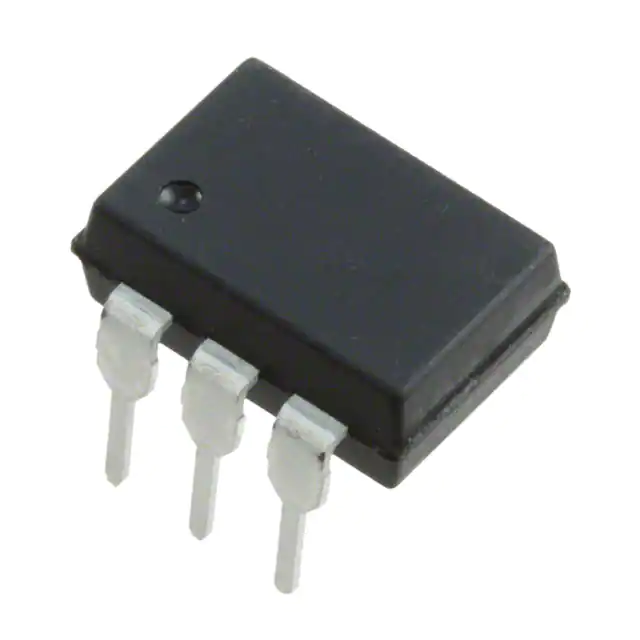
ASSR-5211
High Current, 1 Form A, Solid State Relay (MOSFET)
(600V/0.2A/16Ω)
Data Sheet
Lead (Pb) Free
RoHS 6 fully
compliant
RoHS 6 fully compliant options available;
-xxxE denotes a lead-free product
Description
Features
The ASSR-5211 is specifically designed for high current
applications, commonly found in the industrial equipments. The relay is a solid-state replacement for singlepole, normally-open, (1 Form A) electromechanical relays.
• Compact Solid-State Bi-directional Signal Switch
The ASSR-5211 consists of an AlGaAs infrared lightemitting diode (LED) input stage optically coupled to
a high-voltage output detector circuit. The detector
consists of a high-speed photovoltaic diode array and
driver circuitry to switch on/off two discrete high voltage
MOSFETs. The relay turns on (contact closes) with a
minimum input current of 3mA through the input LED.
The relay turns off (contact opens) with an input voltage
of 0.8V or less.
• 0.2A or 0.4A Current Rating
The ASSR-5211 connection A, as shown in the schematic,
allows the relay to switch either ac or dc loads. The connection B, with its advantages of reduced on-resistance
and higher output current, allows the relays to switch dc
loads only.
The electrical and switching characteristics are specified
over the temperature range of -40°C to +85°C.
• Single Channel Normally-off Single-Pole-Single-Throw
(SPST) Relay
• 600V Output Withstand Voltage
• Low Input Current: CMOS Compatibility
• Low On-Resistance:
2.5Ω Typical for DC-only, 10Ω Typical for AC/DC
• High Speed Switching:
0.7ms (Ton), 0.07ms (Toff ) Typical @ IF = 5mA
• High Transient Immunity: >1kV/μs
• High Input-to-Output Insulation Voltage
(Safety and Regulatory Approvals Pending)
- 3750 VRMS for 1 min per UL1577
- CSA Component Acceptance
- *5000 VRMS/1 Minute rating is for Option X21 only
(Please consult your regional Avago representatives)
Applications
Functional Diagram
• Industrial Controls
• Factory Automation
Opto-isolation
• Data Acquisition
6
1
Truth Table
3
Turn-off
Circuit
2
5
LED
Output
Off
Open
On
Close
• Measuring Instrument
• Medical System
• Security System
• EMR / Reed Relay Replacement
4
CAUTION: It is advised that normal static precautions be taken in handling and assembly
of this component to prevent damage and/or degradation which may be induced by ESD.
�Ordering Table
ASSR-5211 is UL Recognized with 3750 VRMS and 5000 VRMS (option x21*) for 1 minute per UL1577 and is approved
under CSA Components Acceptance Notice #5.
Option
Part
Number
RoHS
Compliant
Package
Surface Mount
Gullwing
300mil
DIP-6
X
X
X
X
Tape & Reel
-001E
ASSR-5211
-301E
-501E
Quantity
50 units per tube
X
1000 units per reel
To order, choose a part number from the part number column and combine with the desired option from the option
column to form an order entry.
Example 1:
ASSR-5211-501E to order product of 300mil DIP-6 Gull Wing Surface Mount package in Tape and Reel packaging
and RoHS Compliant.
x21* - ‘Please consult your regional Avago representatives’
Schematic
Connection A – AC/DC
Opto -isolation
Opto -isolation
6
1
Turn-off
Circuit
2
1
6
2
4
Equivalent
Relay
Diagram
5
Vo
4
3
Connection B – DC Only
Opto -isolation
Opto -isolation
1
6
+
Vo
5
Turn-off
Circuit
2
-
3
4
2
1
4 and 6
2
5
Equivalent
Relay
Diagram
�Package Outline Drawings
ASSR-5211 6-Pin DIP Package
7.36 (0.290)
7.88 (0.310)
9.40 (0.370)
9.90 (0.390)
6
5
TYPE
NUMBER
4
LEAD FREE
YYWW
PIN
ONE
DOT
1
0.20 (0.008)
0.33 (0.013)
DATE CODE
A XXXX
UL
RECOGNITION
RU
2
5° TYP.
3
6.10 (0.240)
6.60 (0.260)
1.78 (0.070) MAX.
4.70 (0.185) MAX.
(0.020)
(0.040)
2.66 (0.105) MIN.
0.45 (0.018)
0.65 (0.025)
2.28 (0.090)
2.80 (0.110)
2.16 (0.085)
2.54 (0.100)
DIMENSIONS IN MILLIMETERS AND (INCHES).
ASSR-5211 6-Pin DIP Package with Gull Wing Surface Mount Option 300
9.65 ± 0.25
(0.380 ± 0.010)
LAND PATTERN RECOMMENDATION
6.35 ± 0.25
(0.250 ± 0.010)
10.9 (0.430)
1.27 (0.050)
1.78
(0.070)
MAX.
2.0 (0.080)
9.65 ± 0.25
(0.380 ± 0.010)
0.635 ± 0.130
(0.025 ± 0.005)
7.62 ± 0.25
(0.300 ± 0.010)
0.20 (0.008)
0.30 (0.013)
4.19
MAX.
(0.165)
2.29
(0.090)
2.54
(0.100)
TYP.
NOTE: FLOATING LEAD PROTRUSION IS 0.25 mm (10 mils) MAX.
3
0.635 ± 0.25
(0.025 ± 0.010)
12° NOM.
�Solder Reflow Temperature Profile
Recommended reflow condition as per JEDEC Standard, J-STD-020 (latest revision). Non-Halide Flux should be used.
Regulatory Information
The ASSR-5211 is approved by the following organizations:
UL
Approved under UL 1577, component recognition program up to VISO = 3750 VRMS and 5000 VRMS (option x21).
CSA
Approved under CSA Component Acceptance Notice #5.
Insulation and Safety Related Specifications
Parameter
Symbol
ASSR-5211
Units
Conditions
Minimum External Air Gap
(Clearance)
L(101)
7.1
mm
Measured from input terminals to output terminals,
shortest distance through air.
Minimum External Tracking
(Creepage)
L(102)
7.4
mm
Measured from input terminals to output terminals,
shortest distance path along body.
0.08
mm
Through insulation distance conductor to conductor,
usually the straight line distance thickness between the
emitter and detector.
175
V
DIN IEC 112/VDE 0303 Part 1
Minimum Internal Plastic Gap
(Internal Clearance)
Tracking Resistance
(Comparative Tracking Index)
Isolation Group (DIN VDE0109)
4
CTI
IIIa
Material Group (DIN VDE 0109)
�Absolute Maximum Ratings
Parameter
Symbol
Min.
Max.
Units
Storage Temperature
TS
-55
125
°C
Operating Temperature
TA
-40
85
°C
125
°C
Temperature
260
°C
Time
10
sec
25
mA
Surge
50
mA
Transient
1000
mA
VR
5
V
PIN
40
mW
PO
640
mW
640
mW
0.2
A
Junction Temperature
Lead Soldering Cycle
Input Current
TJ
Average
IF
Reversed Input Voltage
Input Power Dissipation
Output Power
Dissipation
Average Output Current
(TA=25°C, TC ≤ 100°C)
Output Voltage
(TA=25°C)
Connection A
Connection B
Connection A
IO
Connection B
Connection A
VO
Connection B
0.4
A
- 600
600
V
0
600
V
4
kV
ESD Human Body Model:
MIL-STD-883 Method 3015.7
Solder Reflow Temperature Profile
Note
1
See Lead Free IR Profile
Recommended Operating Conditions
Parameter
Symbol
Min.
Max.
Units
Input Current (ON)
IF(ON)
3
20
mA
Input Voltage (OFF)
VF(OFF)
0
0.8
V
Operating Temperature
TA
-40
+85
°C
Note
Package Characteristics
Unless otherwise specified, operating temperature TA = 25°C.
Parameter
Symbol
Min.
Input-Output Momentary
Withstand Voltage
VISO
3750
Typ.
Max.
Units
Conditions
Note
VRMS
RH ≤ 50%, t = 1min,
TA = 25°C
3, 4
5000
RH ≤ 50%, t = 1min,
TA = 25°C, option x21
Input-Output Resistance
RI-O
1014
Ω
VI-O = 500 Vdc
3
Input-Output Capacitance
CI-O
0.8
pF
VI-O = 0Vdc, f = 1MHz
3
5
�Electrical Specifications (DC)
Over recommended operating TA = - 40°C to 85°C, IF = 5mA to 10mA, unless otherwise specified.
Parameter
Sym.
Min.
Typ.
Max.
Fig.
Note
Output Withstand Voltage
| VO(OFF)|
600
650
V
VF=0.8V, IO=250μA
Output
On-Resistance
Connection A
R(ON)
10
16
Ω
IF=5mA, IO=0.2A,
Pulse ≤30ms, TA=25°C
3
10
6
Connection B
R(ON)
2.5
4
Ω
IF=5mA, IO=0.4A,
Pulse ≤30ms, TA=25°C
11
6
Output Leakage Current
IO(OFF)
0.001
0.1
μA
VF=0.8V, VO=600V, TA=25°C
5
-
Output Off-Capacitance
C(OFF)
500
1
μA
VF=0.8V, VO=550V
4
-
pF
VF=0.8V, VO=0V, f=1MHz
6
-
Output Offset Voltage
| V(OS)|
1
μV
IF=5mA, IO=0mA
V
IR=10μA
V
IF=5mA
7,8
-
550
Input Reverse Breakdown Voltage VR
5
Input Forward Voltage
1.1
VF
1.3
1.7
Units
Conditions
V
VF=0.8V, IO=250μA, TA=25°C
Switching Specifications (AC)
Over recommended operating TA = - 40°C to 85°C, IF = 5mA to 10mA, unless otherwise specified.
Parameter
Sym.
Turn On Time
TON
Min.
Typ.
Max.
Units
Conditions
Fig.
0.7
2.5
ms
IF=5mA, IO=0.2A, TA=25°C
12,16
5.0
ms
IF=5mA, IO=0.2A
13,16
0.4
Turn Off Time
0.07
TOFF
0.06
1.5
ms
IF=10mA, IO=0.2A, TA=25°C
12,16
3.0
ms
IF=10mA, IO=0.2A
13,16
0.5
ms
IF=5mA, IO=0.2A, TA=25°C
14,16
1
ms
IF=5mA, IO=0.2A
15,16
0.2
ms
IF=10mA, IO=0.2A, TA=25°C
14,16
0.5
ms
IF=10mA, IO=0.2A
15,16
Note
Output Transient Rejection
dVO/dt
1
7
kV/μs
ΔVO=600V, RM ≥ 1MΩ,
CM=1000pF, TA=25°C
17
5
Input-Output Transient
Rejection
dVI-O/dt
1
20
kV/μs
VDD=5V, ΔVI-O=1000V,
RL=1kΩ, CL=25pF, TA=25°C
18
5
Notes:
1. For derating, refer to Figure 1 and 2.
2. The voltage across the output terminal of the relay should not exceed this rated withstand voltage. Over-voltage protection circuits should be
added in some applications to protect against over-voltage transients.
3. Device is considered as a two terminal device: pins 1, 2, and 3 shorted together and pins 5, 6, and 7 shorted together.
4. The Input-Output Momentary Withstand Voltage is a dielectric voltage rating that should not be interpreted as an input-output continuous
voltage rating. For the continuous voltage rating refer to the IEC/EN/DIN EN 60747-5-2 Insulation Characteristics Table (if applicable), your
equipment level safety specification, or Avago Application Note 1074, “Optocoupler Input-Output Endurance Voltage.”
5. During the pulsed R(ON) measurement ( IO duration ≤30ms), ambient (TA) and case temperature (TC) are equal.
6. For the transient rejection measurements, refer to Avago whitepaper, AV01-0610EN, “Solid State Relay Transient Immunity”.
6
�0.5
IF = 10mA,
4-Layer
0.2
IO - OUTPUT CURRENT - A
IO - OUTPUT CURRENT - A
0.25
0.15
Safe
Operating
Area
0.1
0.05
0
-40
-20
0
20
40
60
TA - TEMPERATURE - °C
80
IO(OFF) - OUTPUT LEAKAGE CURENT - A
NORMALIZED OUTPUT WITHSTAND VOLTAGE
1.05
1
0.95
0.9
-40
-20
0
20
40
60
TA - TEMPERATURE - °C
80
-20
0
20
40
TA - TEMPERATURE - °C
60
80
100
1.E-08
1.E-09
1.E-10
1.E-11
1.E-12
-40
100
-15
10
35
TA - TEMPERATURE - °C
60
85
Figure 4. Typical Output Leakage Current vs Ambient Temperature
1000
2.5E-04
C OUT - OUTPUT CAPACITANCE - pF
IO(OFF) - OUTPUT LEAKAGE CURRENT - μA
0.1
1.E-07
Figure 3. Normalized Typical Outupt Withstand Voltage vs Temperature
2.0E-04
1.5E-04
1.0E-04
5.0E-05
0
150
300
450
Vo - OUTPUT VOLTAGE - V
Figure 5. Typical Output Leakage Current vs Output Voltage
7
Safe
Operating
Area
0.2
Figure 2. Maximum Output Current Rating vs Ambient Temperature (DC
Connection)
1.1
0.0E+00
0.3
0
-40
100
Figure 1. Maximum Output Current Rating vs Ambient Temperature (AC/DC
Connection)
IF = 10mA,
4-Layer
0.4
600
800
600
400
200
0
0
20
40
60
V O(OFF) - OUTPUT VOLTAGE - V
80
Figure 6. Typical Output Off-State Capacitance vs Output Voltage
100
�20
1.6
18
1.5
I F - FORWARD CURRRENT - mA
V F - FORWARD VOLTAGE - V
1.7
IF = 10mA
1.4
IF = 5mA
1.3
1.2
1.1
1
-40
-20
0
20
40
60
TA - TEMPERATURE - °C
80
10
6
4
2
R ON(AC) - ON-RESISTANCE - Ω
IO - OUTPUT CURRENT - A
T A = -40 °C
T A = 25 °C
0.05
0.00
T A = 85 °C
-0.05
-0.10
-0.15
-3
-2
-1
0
1
V O - OUTPUT VOLTAGE - V
2
1
1.2
1.4
V F - FORWARD VOLTAGE - V
1.6
1.8
15
I F = 5mA
10
I F = 10mA
5
0
3
Figure 9. Typical Output Current vs Output Voltage
10
1500
8
1200
I F = 5mA
6
4
2
I F = 10mA
-50
-25
0
-50
-25
0
25
50
75
TA - TEMPERATURE - °C
100
125
Figure 10. Typical On Resistance (AC/DC Connection) vs Temperature
TON - TURN ON TIME - μS
RON(DC) - ON-RESISTANCE - Ω
0.8
20
0.15
25
50
75
TA -TEMPERATURE - °C
100
Figure 11. Typical On Resistance (DC Connection) vs Temperature
8
T A = 85 °C
8
Figure 8. Typical Forward Current vs Forward Voltage
0.10
0
T A = 25 °C
12
0.20
-0.20
T A = 0 °C
14
100
Figure 7. Typical Forward Voltage vs Ambient Temperature
T A =-40 °C
16
125
900
600
300
0
5
10
15
IF - CONTROL CURRENT - mA
Figure 12. Typical Turn On Time vs Input Current
20
�100
800
I F = 5mA
TOFF - TURN OFF TIME - μS
T ON - TURN ON TIME - μs
1000
600
400
IF = 10mA
200
0
-40
-20
0
20
40
60
TA - TEMPERATURE - °C
80
80
60
40
20
0
100
Figure 13. Typical Turn On Time vs Temperature
5
10
15
IF - CONTROL CURRENT - mA
20
Figure 14. Typical Turn Off Time vs Input Current
T OFF - TURN OFF TIME - μ-s
100
80
I F = 5mA
60
I F = 10mA
40
20
0
-40
-20
0
20
40
60
TA -TEMPERATURE- o C
80
100
Figure 15. Typical Turn Off Time vs Temperature
PULSE GEN.
Zo = 50Ω
tf=tr=5ns
VDD
RL
IF
1
INPUT
MONITORING
NODE
R
200ohm
9
6
2
5
3
4
Figure 16 Switching Circuit for TON, TOFF
50%
50%
ASSR-5211
C L* OUTPUT Vo
MONITORING
NODE
(*CLIS APPROXIMATELY
25pF WHICH INCLUDES
PROBE AND STRAY
WIRING CAPACITANCE)
OUTPUT
IF
P.W. = 10ms
90%
OUTPU T
Vo
10%
tON
tOFF
�OUTPUT Vo
MONITORING
NODE
ASSR-5211
1
INPUT OPEN
6
5
2
VPEAK
CM=1nF
4
3
RM=1Mohm
+
PULSE GEN
Zo = 50
CM INCLUDES PROBE AND FIXTURE CAPACITANCE
RM INCLUDES PROBE AND FIXTURE RESISTANCE
90%
90%
VPEAK
10%
10%
tR
tF
VO(MAX)< 0.6V
dV0
dt
=
( 0 . 8 ) VPEAK
tR
OR
( 0 . 8 ) VPEAK
OVER SHOOT ON VPEAK IS TO BE 10%
Figure 17 Test Circuit for Output Transient Immunity
10
tF
�VDD = 5V
IF
ASSR-5211
B
1
RL = 1koh m
6
CL*
A
2
5
3
4
OUTPUT Vo
MONITORING
NODE
(*CLIS APPROXIMATELY 25pF WHICH
INCLUDES PROBE AND STRAY WIRING
CAPACITANCE)
+
V FF
VI-O
+
PULSE GEN.
Zo = 50Ω
90%
90%
VI-O(PEAK)
10%
10%
tR
tF
VO(OFF)
VO(OFF) (min)> 4V
SWITCH AT POSITION ‘A’: IF = 0mA
VO(ON) (min)> 0.8V
VO(ON)
SWITCH AT POSITION ‘B’: IF = 5mA
Figure 18 . Test Circuit for Input-Output Transient Immunity
For product information and a complete list of distributors, please go to our web site:
www.avagotech.com
Avago, Avago Technologies, and the A logo are trademarks of Avago Technologies in the United States and other countries.
Data subject to change. Copyright © 2005-2012 Avago Technologies. All rights reserved.
AV02-0152EN - March 19, 2012
�