ASSR-V621 and ASSR-V622
Dual Channel Photovoltaic MOSFET Driver
(6.5V/15μA)
Data Sheet
Lead (Pb) Free
RoHS 6 fully
compliant
RoHS 6 fully compliant options available;
-xxxE denotes a lead-free product
Description
Features
The ASSR-V62X Series is specially designed to drive high
power MOSFETs. It consists of an AlGaAs infrared lightemitting diode (LED) input stage optically coupled to an
output detector circuit. The detector consists of a highspeed photovoltaic diode array and driver circuitry to
switch on/off two discrete high voltage MOSFETs externally. The relay driver turns on (contact closes) with a minimum input current of 3mA through the input LED. The
relay driver turns off (contact opens) with an input voltage
of 0.8V or less.
• Dual Channel Photovoltaic MOSFET Driver
The dual channel configurations, ASSR-V621 and ASSRV622, allow 2 independent MOSFETs to be driven. It has
the versatility to double the photovoltaic voltage by connecting the 2 channels in series or to double the short
circuit current by connecting the 2 channels in parallel.
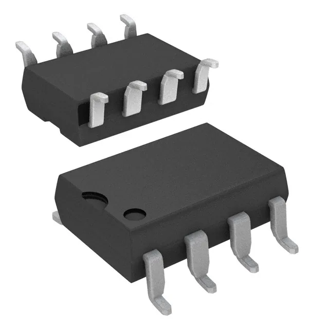
They are available in 8-pin DIP and Gull Wing Surface
Mount packages.
• Open Circuit Voltage: 7V Typical
• Short Circuit Current: 20mA Typical
• Low Input Current: CMOS Compatibility
• Fast Switching Speed:
0.3ms (Ton), 0.03ms (Toff ) Typical
• High Input-to-Output Insulation Voltage
(Safety and Regulatory Pending Approvals)
- 3750 Vrms for 1 min per UL1577
- CSA Component Acceptance
Applications
• Solid State Relay Module
• Voltage Supply for electronic circuits
CAUTION: It is advised that normal static precautions be taken in handling and assembly
of this component to prevent damage and/or degradation which may be induced by ESD.
�Ordering Information
ASSR-xxxx is UL Recognized with 3750 Vrms for 1 minute per UL1577 and is approved under CSA Component Acceptance Notice #5, File CA 88324.
Option
Part number
RoHS Compliant
Package
Surface
Mount
Gull
Wing
300 mil DIP-8
X
X
X
X
X
X
X
X
Tape
& Reel
-002E
ASSR-V621
-302E
50 units per tube
-502E
50 units per tube
X
-002E
ASSR-V622
-302E
Quantity
1000 units per reel
50 units per tube
300 mil DIP-8
-502E
50 units per tube
X
1000 units per reel
To order, choose a part number from the part number column and combine with the desired option from the option
column to form an order entry.
Example:
ASSR-V621-002E to order product of 300mil DIP-8 package in tube packaging and RoHS Compliant.
Option datasheets are available. Contact your Avago sales representative or authorized distributor for information.
Schematic
Opto-isolation
Opto-isolation
8
1
2
7
2
7
3
6
3
6
5
4
1
Turn-off
Circuit
Turn-off
Circuit
Turn-off
Circuit
Turn-off
Circuit
4
ASSR-V621-002E
�
8
5
ASSR-V622-002E
�Package Outline Drawings
8-Pin DIP Package
7.62 ± 0.25
(0.300 ± 0.010)
9.65 ± 0.25
(0.380 ± 0.010)
8
TYPE NUMBER
7
6
5
DATE CODE
A XXXX
LEAD FREE
6.35 ± 0.25
(0.250 ± 0.010)
OPTION CODE*
YYWW RU
1
2
3
UL
RECOGNITION
4
1.78 (0.070) MAX.
1.19 (0.047) MAX.
5° TYP.
3.56 ± 0.13
(0.140 ± 0.005)
4.70 (0.185) MAX.
+ 0.076
0.254 - 0.051
+ 0.003)
(0.010 - 0.002)
0.51 (0.020) MIN.
2.92 (0.115) MIN.
DIMENSIONS IN MILLIMETERS AND (INCHES).
OPTION NUMBERS 300 AND 500 NOT MARKED.
0.65 (0.025) MAX.
1.080 ± 0.320
(0.043 ± 0.013)
2.54 ± 0.25
(0.100 ± 0.010)
8-Pin DIP Package with Gull Wing Surface Mount Option 300
LAND PATTERN RECOMMENDATION
9.65 ± 0.25
(0.380 ± 0.010)
8
7
6
1.016 (0.040)
5
6.350 ± 0.25
(0.250 ± 0.010)
1
2
3
10.9 (0.430)
4
1.27 (0.050)
1.19
(0.047)
MAX.
1.780
(0.070)
MAX.
9.65 ± 0.25
(0.380 ± 0.010)
7.62 ± 0.25
(0.300 ± 0.010)
3.56 ± 0.13
(0.140 ± 0.005)
1.080 ± 0.320
(0.043 ± 0.013)
0.635 ± 0.25
(0.025 ± 0.010)
0.635 ± 0.130
2.54
(0.025 ± 0.005)
(0.100)
BSC
DIMENSIONS IN MILLIMETERS (INCHES).
LEAD COPLANARITY = 0.10 mm (0.004 INCHES).
NOTE: FLOATING LEAD PROTRUSION IS 0.25 mm (10 mils) MAX.
�
2.0 (0.080)
+ 0.076
0.254 - 0.051
+ 0.003)
(0.010 - 0.002)
12° NOM.
�Lead Free IR Profile
tp
TEMPERATURE (°C)
Tp
TL
260 +0/-5°C
TIME WITHIN 5°C of ACTUAL
PEAK TEMPERATURE
20-40 SEC.
217°C
RAMP-UP
3°C/SEC. MAX.
150 - 200°C
T smax
RAMP-DOWN
6°C/SEC. MAX.
T smin
ts
PREHEAT
60 to 180 SEC.
tL
60 to 150 SEC.
25
t 25°C to PEAK
TIME (SECONDS)
NOTES:
THE TIME FROM 25°C to PEAK TEMPERATURE = 8 MINUTES MAX.
Tsmax = 200°C, Tsmin = 150°C
Use of non-chlorine-activated fluxes is highly recommended.
Note: Non-Halide flux should be used.
Regulatory Information
The ASSR-V621-002E and ASSR-V622-002E are approved by the following organizations:
UL
Approved under UL 1577, component recognition program up to VISO = 3750 VRMS
Approved under CSA Component Acceptance Notice #5.
Insulation and Safety Related Specifications
Parameter
Symbol
ASSR-V621-002E
ASSR-V622-002E
Units
Conditions
Minimum External Air
Gap (Clearance)
L(101)
7.1
mm
Measured from input terminals to output terminals,
shortest distance through air.
Minimum External Tracking
(Creepage)
L(102)
7.4
mm
Measured from input terminals to output terminals,
shortest distance path along body.
0.08
mm
Through insulation distance conductor to conductor,
usually the straight line distance thickness between
the emitter and detector.
175
V
DIN IEC 112/VDE 0303 Part 1
Minimum Internal Plastic
Gap (Internal Clearance)
Tracking Resistance
(Comparative Tracking
Index)
Isolation Group
(DIN VDE0109)
�
CTI
IIIa
Material Group (DIN VDE 0109)
�Absolute Maximum Ratings
Parameter
Symbol
Min.
Max.
Units
Storage Temperature
TS
-55
125
°C
Operating Temperature
TA
-40
85
°C
260
°C
10
s
30
mA
Lead Soldering Cycle
Temperature
Time
Input Current
Average
IF
Surge
300
Transient
1000
Reversed Input Voltage
VR
5
V
Input Power Dissipation
PIN
100
mW
Solder Reflow Temperature Profile
See Lead Free IR Profile
Note
Recommended Operating Conditions
Parameter
Symbol
Min.
Max.
Units
Input Current (ON)
IF(ON)
3
30
mA
Input Voltage (OFF)
VF(OFF)
0
0.8
V
Operating Temperature
TA
-40
+85
°C
Note
Package Characteristics
Unless otherwise specified, operating temperature TA = 25°C.
Parameter
Symbol
Min.
Input-Output Momentary
Withstand Voltage
VISO
3750
Input-Output Resistance
RI-O
Input-Output Capacitance
CI-O
Typ.
Max.
Units
Conditions
Vrms
RH ≤ 50%, t = 1 min
1012
Ω
VI-O = 500 Vdc
0.6
pF
f = 1 MHz; VI-O = 0 Vdc
Fig.
Note
1
Electrical Specifications (DC)
For operating TA = +25°C
Parameter
Symbol
Min.
Typ.
Open Circuit Voltage
VOC
6.5
Short Circuit Current
ISC
15
Input Reverse Breakdown
Voltage
VR
5
Input Forward Voltage
VF
1.1
Units
Conditions
7
V
IF =10mA, IO=0mA
20
mA
IF =10mA, VO=0V
V
IR =10mA
V
IF =10mA
Parameter
Symbol
Min.
Units
Conditions
Turn On Time
TON
0.28
ms
IF =10mA, CL=1nF
Turn Off Time
TOFF
0.03
ms
IF =10mA, CL=1nF
1.3
Max.
1.7
Fig.
Note
Switching Specifications (AC)
For operating TA = +25°C
Typ.
Max.
Note:
1. Device is considered as a two terminal device; pin 1, 2, 3, 4 shorted and pin 5, 6, 7, 8 shorted.
�
Fig.
Note
�VOC - OPEN CIRCUIT OUTPUT VOLTAGE - V
ISC-SHORTCIRCUITOUTPUTCURRENT- µA
70
60
IF=30mA
50
40
IF=20mA
30
20
IF=10mA
10
0
-50
IF=5mA
-25
IF=3mA
0
25
50
TA - TEMPERATURE - °C
75
100
6
IF=5mA
IF=3mA
2
0
-50
40
TOFF - TURN OFF TIME - µs
500
IF=10mA
300
200
100
-25
IF=10mA
4
50
0
-50
IF=20mA
8
600
400
IF=30mA
-25
0
25
50
TA - TEMPERATURE - °C
75
100
Figure 2. VOC vs Temperature
Figure 1. Short Circuit Output Current vs
TON - TURN ON TIME - µs
10
0
25
50
TA - TEMPERATURE - °C
75
100
Figure 3. TON vs Temperature
For product information and a complete list of distributors, please go to our web site:
IF=10mA
30
20
10
0
-50
-25
Figure 4. TOFF vs Temperature
www.avagotech.com
Avago, Avago Technologies, and the A logo are trademarks of Avago Technologies in the United States and other countries.
Data subject to change. Copyright © 2005-2008 Avago Technologies. All rights reserved.
AV02-0259EN - July 18, 2008
0
25
50
TA - TEMPERATURE - °C
75
100
�