Agilent AT-41511, AT-41533
General Purpose, Low Noise
NPN Silicon Bipolar Transistors
Data Sheet
Features
Description
Agilent’s AT-41511 and AT-41533
are general purpose NPN bipolar
transistors that offer excellent
high frequency performance at an
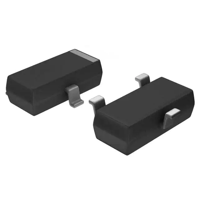
economical price. The AT-41533
uses the 3 lead SOT-23, while the
AT-41511 places the same die in
the lower parasitic 4 lead
SOT-143. Both packages are
industry standard, and compatible
with high volume surface mount
assembly techniques.
Outline Drawing
EMITTER COLLECTOR
415
BASE
EMITTER
SOT 143 (AT-41511)
COLLECTOR
415
The 4 micron emitter-to-emitter
pitch of these transistors yields
high performance products that
can perform a multiplicity of
tasks. The 14 emitter finger
interdigitated geometry yields an
intermediate-sized transistor with
easy to match to impedances, low
noise figure, and moderate power.
Optimized for best performace
from a 5 to 8 volt bias supply,
these transistors are also good
performers at 2.7 V. Applications
include use in wireless systems as
an LNA, gain stage, buffer,
oscillator, or active mixer.
An optimum noise match near
50 ohms at 900 MHz makes these
devices particularly easy to use as
LNAs. Typical amplifier designs
at 900 MHz yield 1 dB noise
figures with 15 dB or more
BASE
EMITTER
SOT 23 (AT-41533)
associated gain at a 5 V, 5 mA
bias, with good gain and noise
figure obtainable at biases as low
as 2 mA.
The AT-415 series bipolar
transistors are fabricated using
Agilent’s 10 GHz fT Self-AlignedTransistor (SAT) process. The die
are nitride passivated for surface
protection. Excellent device
uniformity, performance and
reliability are produced by the
use of ion-implantation, selfalignment techniques, and gold
metalization in the fabrication of
these devices.
• General Purpose NPN
Bipolar Transistor
• 900 MHz Performance:
AT-41511: 1 dB NF, 15.5 dB GA
AT-41533: 1 dB NF, 14.5 dB GA
• Characterized for 3, 5, and
8 Volt Use
• SOT-23 and SOT-143 SMT
Plastic Packages
• Tape-and-Reel Packaging
Option Available
• Lead-free Option Available
�2
AT-41511, AT-41533 Absolute Maximum Ratings
Units
Absolute
Maximum[1]
VEBO
Emitter-Base Voltage
V
1.5
VCBO
Collector-Base Voltage
V
20
VCEO
Collector-Emitter Voltage
Symbol
Parameter
V
12
IC
Collector Current
mA
50
PT
Power Dissipation[2,3]
mW
225
Tj
Junction Temperature
°C
150
TSTG
Storage Temperature
°C
-65 to 150
Thermal Resistance:[2]
θjc =550°C/W
Notes:
1. Operation of this device above any one
of these parameters may cause
permanent damage.
2. TMounting Surface = 25°C.
3. Derate at 1.82 mW/°C for TC > 26°C.
Electrical Specifications, TA = 25°C
AT-41511
Symbol
Parameters and Test Conditions
Units Min
30
AT-41533
Typ
Max
Min
Typ
Max
150
270
30
150
270
hFE
Forward Current Transfer Ratio
VCE = 5 V
IC = 5 mA
-
ICBO
Collector Cutoff Current
VCB = 3 V
µA
0.2
0.2
IEBO
Emitter Cutoff Current
VEB = 1 V
µA
1.0
1.0
Characterization Information, TA = 25°C
AT-41511 AT-41533
Symbol
Parameters and Test Conditions
Units
Min Typ Min Typ
NF
Noise Figure
VCE = 5 V, IC = 5 mA
f = 0.9 GHz
f = 2.4 GHz
dB
1.0
1.7
1.0
1.6
GA
Associated Gain
VCE = 5 V, IC = 5 mA
f = 0.9 GHz
f = 2.4 GHz
dB
15.5
11
14.5
9
P1dB
Power at 1 dB Gain Compression (opt tuning)
VCE = 5 V, IC = 25 mA
f = 0.9 GHz
dBm
14.5
14.5
G1dB
Gain at 1 dB Gain Compression (opt tuning)
VCE = 5 V, IC = 25 mA
f = 0.9 GHz
dB
17.5
14.5
Output Third Order Intercept Point,
VCE = 5 V, IC =25 mA (opt tuning)
f = 0.9 GHz
dBm
25
25
Gain in 50 Ω system; VCE = 5 V, IC = 5 mA
f = 0.9 GHz
f = 2.4 GHz
dB
13.5 15.5 10.8
7.9
12.8
5.2
IP3
|S21E|2
�3
AT-41511, AT-41533 Typical Performance
3.0
3.0
3.0
25 mA
25 mA
2.5
10 mA
1.5
2, 5 mA
1.0
2.5
2 mA
2.0
10 mA
1.5
5 mA
1.0
0.5
0.5
0.6
1.1
1.6
2.1
0
0.1
2.6
10 mA
1.5
5 mA
1.0
1.6
2.1
0
0.1
2.6
0.6
FREQUENCY (GHz)
25
20
15
Ga (dB)
Ga PKG 33 (dB)
10, 25 mA
5 mA
2 mA
15
PKG 33
10, 25 mA
5 mA
10, 25 mA
5 mA
10
PKG 33
10, 25 mA
5 mA
10, 25 mA
5 mA
10
5
5
10
5
2.6
PKG 11
15
20
PKG 11
2.1
20
20
10, 25 mA
2 mA
1.6
Figure 3. AT-41511 and AT-41533
Minimum Noise Figure vs. Frequency
and Current at VCE = 8 V.
PKG 11
5 mA
1.1
FREQUENCY (GHz)
Figure 2. AT-41511 and AT-41533
Minimum Noise Figure vs. Frequency
and Current at VCE = 5 V.
Figure 1. AT-41511 and AT-41533
Minimum Noise Figure vs. Frequency
and Current at VCE = 2.7 V.
PKG 33
0
0.1
1.1
0.6
1.6
2.1
0
0.1
5
2.6
1.1
0.6
1.6
2.1
0
0.1
2.6
2.1
2.6
20
20
20
1.6
Figure 6. AT-41511 and AT-41533
Associated Gain vs. Frequency and
Current at VCE = 8 V.
Figure 5. AT-41511 and AT-41533
Associated Gain vs. Frequency and
Current at VCE = 5 V.
Figure 4. AT-41511 and AT-41533
Associated Gain vs. Frequency and
Current at VCE = 2.7 V.
1.1
0.6
FREQUENCY (GHz)
FREQUENCY (GHz)
FREQUENCY (GHz)
25 mA
15
15
15
10
10 mA
5 mA
5
0
0.1
0.6
1.1
1.6
2.1
FREQUENCY (GHz)
Figure 7. AT-41511 and AT-41533
P1dB vs. Frequency and Bias at
VCE = 2.7 V, with Optimal Tuning.
2.6
10 mA
10
5 mA
10 mA
10
5 mA
5
5
0
0.1
P1 dB (dBm)
25 mA
P1 dB (dBm)
25 mA
P1 dB (dBm)
Ga PKG 11 (dB)
1.1
0.6
FREQUENCY (GHz)
10
25 mA
2.0
0.5
Ga (dB)
0
0.1
15
NOISE FIGURE (dB)
2.0
NOISE FIGURE (dB)
NOISE FIGURE (dB)
2.5
0.6
1.1
1.6
2.1
FREQUENCY (GHz)
Figure 8. AT-41511 and AT-41533
P1dB vs. Frequency and Bias at
VCE = 5 V, with Optimal Tuning.
2.6
0
0.1
0.6
1.1
1.6
2.1
FREQUENCY (GHz)
Figure 9. AT-41511 and AT-41533
P1dB vs. Frequency and Bias at
VCE = 8 V, with Optimal Tuning.
2.6
�4
AT-41511 Typical Scattering Parameters, Common Emitter, Zo = 50 Ω, VCE = 2.7 V, IC = 5 mA
Freq.
GHz
Mag
S11
Ang
dB
S21
Mag
Ang
dB
S12
Mag
Ang
Mag
S22
Ang
0.1
0.5
0.9
1.0
1.5
1.8
2.0
2.4
3.0
4.0
5.0
0.84
0.59
0.49
0.48
0.46
0.46
0.46
0.47
0.5
0.56
0.61
-27
-102
-141
-149
-176
170
162
148
130
106
87
23.44
19.01
15.09
14.30
11.15
9.69
8.86
7.37
5.58
3.25
1.36
14.854
8.924
5.684
5.189
3.61
3.051
2.774
2.337
1.901
1.454
1.17
161
115
93
89
72
64
59
50
36
17
0
-34.89
-24.88
-22.97
-22.73
-21.21
-20.26
-19.74
-18.64
-17.14
-14.89
-12.96
0.018
0.057
0.071
0.073
0.087
0.097
0.103
0.117
0.139
0.18
0.225
76
48
43
43
44
45
45
46
45
42
37
0.95
0.65
0.51
0.49
0.44
0.43
0.42
0.42
0.41
0.4
0.4
-11
-34
-39
-39
-43
-45
-47
-51
-59
-73
-91
30
20
Freq
Fmin
GHz
dB
Mag
Ang
-
0.1
0.9
1.8
2.4
0.8
1.0
1.4
1.7
0.45
0.39
0.32
0.40
6
63
137
177
0.25
0.19
0.12
0.09
GAIN (dB)
Γopt
MSG
25
AT-41511 Typical Noise Parameters,
Common Emitter, Zo = 50 Ω, VCE = 2.7 V, IC = 5 mA
Rn
15
MAG
10
MSG
S21
5
0
0
2
1
3
4
5
FREQUENCY (GHz)
Figure 10. AT-41511 Gains vs.
Frequency at VCE = 2.7 V, IC = 5 mA.
AT-41533 Typical Scattering Parameters, Common Emitter, Zo = 50 Ω, VCE = 2.7 V, IC = 5 mA
Freq.
GHz
Mag
S11
Ang
dB
S21
Mag
Ang
dB
S12
Mag
Ang
Mag
S22
Ang
0.1
0.5
0.9
1.0
1.5
1.8
2.0
2.4
3.0
4.0
5.0
0.78
0.35
0.23
0.21
0.20
0.22
0.23
0.26
0.30
0.37
0.44
-30
-99
-144
-154
162
144
134
118
101
80
62
23.43
16.91
12.50
11.65
8.50
7.09
6.30
4.97
3.45
1.66
0.35
14.834
7.004
4.219
3.826
2.661
2.261
2.065
1.773
1.488
1.211
1.041
155
103
84
80
64
56
51
42
30
13
-1
-33.98
-24.58
-21.21
-20.54
-17.46
-15.97
-15.09
-13.39
-11.21
-8.20
-5.90
0.020
0.059
0.087
0.094
0.134
0.159
0.176
0.214
0.275
0.389
0.507
75
60
62
63
64
63
63
61
56
46
33
0.94
0.62
0.55
0.54
0.52
0.51
0.51
0.50
0.48
0.45
0.42
-12
-28
-30
-31
-36
-40
-42
-48
-58
-80
-104
30
AT-41533 Typical Noise Parameters,
Common Emitter, Zo = 50 Ω, VCE = 2.7 V, IC = 5 mA
Fmin
GHz
dB
0.1
0.9
1.8
2.4
0.7
1.0
1.4
1.6
Γopt
Mag
0.45
0.25
0.38
0.54
Rn
Ang
8
94
-159
-122
MSG
20
0.20
0.13
0.08
0.16
GAIN (dB)
Freq
25
15
MAG
10
MSG
S21
5
0
0
1
2
3
4
5
FREQUENCY (GHz)
Figure 11. AT-41533 Gains vs.
Frequency at VCE = 2.7 V, IC = 5 mA.
�5
AT-41511 Typical Scattering Parameters, Common Emitter, Zo = 50 Ω, VCE = 2.7 V, IC = 25 mA
Freq.
GHz
Mag
S11
Ang
dB
S21
Mag
Ang
dB
S12
Mag
Ang
Mag
S22
Ang
0.1
0.5
0.9
1.0
1.5
1.8
2.0
2.4
3.0
4.0
5.0
0.49
0.53
0.53
0.53
0.54
0.55
0.56
0.57
0.60
0.64
0.67
-91
-168
172
169
153
145
140
129
116
95
79
29.26
18.55
13.62
12.73
9.34
7.86
6.97
5.47
3.67
1.30
-0.58
29.048
8.459
4.798
4.330
2.932
2.473
2.232
1.877
1.525
1.162
0.935
136
92
79
76
63
57
52
44
32
14
-1
-37.72
-30.46
-26.56
-25.68
-22.50
-21.01
-20.09
-18.49
-16.54
-13.98
-11.90
0.013
0.030
0.047
0.052
0.075
0.089
0.099
0.119
0.149
0.200
0.254
62
61
66
67
67
66
66
64
59
51
43
0.73
0.45
0.42
0.42
0.42
0.42
0.42
0.42
0.41
0.40
0.39
-22
-23
-26
-27
-34
-38
-41
-48
-58
-75
-96
30
AT-41511 Typical Noise Parameters,
Common Emitter, Zo = 50 Ω, VCE = 2.7 V, IC = 25 mA
20
Freq
Fmin
GHz
dB
Mag
Ang
-
0.1
0.9
1.8
2.4
1.6
1.9
2.3
2.7
0.13
0.24
0.40
0.50
18
-162
-137
-122
0.16
0.13
0.23
0.35
GAIN (dB)
Γopt
MSG
25
Rn
15
MAG
10
MSG
S21
5
0
0
2
1
3
4
5
FREQUENCY (GHz)
Figure 12. AT-41511 Gains vs.
Frequency at VCE = 2.7 V, IC = 25 mA.
AT-41533 Typical Scattering Parameters, Common Emitter, Zo = 50 Ω, VCE = 2.7 V, IC = 25 mA
Freq.
GHz
Mag
S11
Ang
dB
S21
Mag
Ang
dB
S12
Mag
Ang
Mag
S22
Ang
0.1
0.5
0.9
1.0
1.5
1.8
2.0
2.4
3.0
4.0
5.0
0.34
0.19
0.20
0.20
0.24
0.25
0.27
0.29
0.33
0.39
0.45
-75
-168
161
154
132
121
115
105
93
76
60
29.37
17.63
12.73
11.84
8.56
7.12
6.32
4.99
3.46
1.69
0.40
29.404
7.614
4.329
3.909
2.679
2.271
2.071
1.777
1.489
1.215
1.047
127
88
74
71
59
52
47
39
27
11
-3
-37.08
-25.68
-20.82
-19.91
-16.42
-14.85
-13.94
-12.32
-10.31
-7.66
-5.73
0.014
0.052
0.091
0.101
0.151
0.181
0.201
0.242
0.305
0.414
0.517
72
76
74
74
70
67
65
61
54
42
29
0.71
0.47
0.46
0.45
0.45
0.44
0.44
0.43
0.41
0.37
0.33
-21
-20
-24
-26
-33
-38
-41
-48
-59
-81
-106
30
MSG
25
AT-41533 Typical Noise Parameters,
Common Emitter, Zo = 50 Ω, VCE = 2.7 V, IC = 25 mA
Freq
Fmin
Rn
GHz
dB
Mag
Ang
-
0.1
0.9
1.8
2.4
1.3
1.6
1.9
2.1
0.10
0.25
0.48
0.59
24
-158
-122
-101
0.12
0.11
0.19
0.37
GAIN (dB)
Γopt
20
15
MAG
10
MSG
S21
5
0
0
1
2
3
4
5
FREQUENCY (GHz)
Figure 13. AT-41533 Gains vs.
Frequency at VCE = 2.7 V, IC = 25 mA.
�6
AT-41511 Typical Scattering Parameters, Common Emitter, Zo = 50 Ω, VCE = 5 V, IC = 5 mA
Freq.
GHz
Mag
S 11
Ang
dB
S21
Mag
Ang
dB
S12
Mag
Ang
Mag
S22
Ang
0.1
0.5
0.9
1.0
1.5
1.8
2.0
2.4
3.0
4.0
5.0
0.88
0.61
0.50
0.48
0.45
0.45
0.45
0.45
0.48
0.53
0.58
-25
-96
-135
-142
-170
176
168
154
136
111
92
23.47
19.31
15.49
14.70
11.59
10.13
9.31
7.85
6.06
3.77
1.91
14.918
9.234
5.948
5.433
3.796
3.210
2.921
2.469
2.009
1.544
1.246
162
116
94
90
74
66
61
52
39
19
2
-34.89
-25.04
-23.22
-22.85
-21.31
-20.45
-19.91
-18.86
-17.33
-15.09
-13.07
0.018
0.056
0.069
0.072
0.086
0.095
0.101
0.114
0.136
0.176
0.222
77
49
44
43
44
45
46
46
46
43
39
0.95
0.66
0.52
0.50
0.45
0.44
0.43
0.42
0.42
0.40
0.40
-11
-33
-38
-39
-42
-44
-46
-51
-58
-72
-90
30
AT-41511 Typical Noise Parameters,
Common Emitter, Zo = 50 Ω, VCE = 5 V, IC = 5 mA
Fmin
GHz
dB
0.1
0.9
1.8
2.4
0.8
1.0
1.4
1.7
Mag
Rn
Ang
0.46
0.39
0.34
0.39
MSG
20
Γopt
GAIN (dB)
Freq
25
-
5
60
130
173
15
MAG
10
0.30
0.22
0.13
0.09
MSG
S21
5
0
0
2
1
3
4
5
FREQUENCY (GHz)
Figure 14. AT-41511 Gains vs.
Frequency at VCE = 5 V, IC = 5 mA.
AT-41533 Typical Scattering Parameters, Common Emitter, Zo = 50 Ω, VCE = 5 V, IC = 5 mA
Freq.
GHz
Mag
S11
Ang
dB
S21
Mag
Ang
dB
S12
Mag
Ang
Mag
S22
Ang
0.1
0.5
0.9
1.0
1.5
1.8
2.0
2.4
3.0
4.0
5.0
0.79
0.36
0.22
0.20
0.18
0.19
0.21
0.24
0.28
0.35
0.42
-28
-94
-137
-148
165
145
134
118
100
80
61
23.48
17.15
12.77
11.93
8.77
7.34
6.56
5.22
3.68
1.87
0.52
14.932
7.200
4.349
3.948
2.746
2.328
2.128
1.823
1.527
1.240
1.062
155
104
84
81
65
58
53
44
32
14
0
-34.89
-25.35
-21.94
-21.21
-18.20
-16.65
-15.70
-14.02
-11.77
-8.61
-6.18
0.018
0.054
0.080
0.087
0.123
0.147
0.164
0.199
0.258
0.371
0.491
76
61
63
64
65
65
65
63
59
50
37
0.95
0.65
0.58
0.57
0.56
0.55
0.55
0.54
0.53
0.50
0.47
-11
-25
-27
-29
-34
-37
-39
-45
-55
-74
-97
30
AT-41533 Typical Noise Parameters,
Common Emitter, Zo = 50 Ω, VCE = 5 V, IC = 5 mA
MSG
20
Freq
Fmin
Rn
GHz
dB
Mag
Ang
-
0.1
0.9
1.8
2.4
0.7
1.0
1.4
1.6
0.46
0.29
0.36
0.53
7
86
-163
-126
0.21
0.13
0.07
0.15
GAIN (dB)
Γopt
25
15
MAG
10
MSG
S21
5
0
0
1
2
3
4
5
FREQUENCY (GHz)
Figure 15. AT-41533 Gains vs.
Frequency at VCE = 5 V, IC = 5 mA.
�7
AT-41511 Typical Scattering Parameters, Common Emitter, Zo = 50 Ω, VCE = 5 V, IC = 25 mA
Freq.
GHz
Mag
S11
Ang
dB
S21
Mag
Ang
dB
S12
Mag
Ang
Mag
S22
Ang
0.1
0.5
0.9
1.0
1.5
1.8
2.0
2.4
3.0
4.0
5.0
0.51
0.46
0.47
0.47
0.48
0.49
0.49
0.51
0.54
0.59
0.63
-74
-161
177
173
157
148
142
132
118
97
81
30
20
15
14
11
9
9
7
5
3
1
32.792
10.259
5.830
5.257
3.553
2.983
2.692
2.254
1.825
1.386
1.113
140
95
80
78
65
58
54
46
34
16
0
-39
-31
-27
-27
-23
-22
-21
-19
-17
-15
-13
0.011
0.028
0.043
0.047
0.068
0.081
0.090
0.108
0.135
0.183
0.234
65
62
66
67
68
68
67
65
61
54
47
0.80
0.51
0.48
0.48
0.47
0.48
0.48
0.48
0.47
0.46
0.46
-19
-21
-23
-24
-30
-34
-36
-42
-51
-66
-84
30
AT-41511 Typical Noise Parameters,
Common Emitter, Zo = 50 Ω, VCE = 5 V, IC = 25 mA
25
20
Freq
Fmin
GHz
dB
Mag
Ang
-
0.1
0.9
1.8
2.4
1.6
1.9
2.3
2.7
0.08
0.11
0.28
0.39
14
165
-153
-134
0.18
0.16
0.18
0.22
GAIN (dB)
Γopt
MSG
Rn
MAG
15
MSG
10
S21
5
0
0
2
1
4
3
5
FREQUENCY (GHz)
Figure 16. AT-41511 Gains vs.
Frequency at VCE = 5 V, IC = 25 mA.
AT-41533 Typical Scattering Parameters, Common Emitter, Zo = 50 Ω, VCE = 5 V, IC = 25 mA
Freq.
GHz
Mag
S11
Ang
dB
S21
Mag
Ang
dB
S12
Mag
Ang
Mag
S22
Ang
0.1
0.5
0.9
1.0
1.5
1.8
2.0
2.4
3.0
4.0
5.0
0.37
0.13
0.13
0.13
0.17
0.19
0.20
0.23
0.27
0.33
0.39
-62
-153
163
154
128
117
111
102
90
76
60
30.00
18.46
13.56
12.68
9.38
7.93
7.14
5.80
4.25
2.48
1.19
31.606
8.375
4.764
4.305
2.945
2.493
2.274
1.949
1.632
1.331
1.147
129
89
76
73
61
54
50
42
31
14
-1
-37.72
-26.20
-21.31
-20.45
-16.95
-15.39
-14.47
-12.84
-10.84
-8.13
-6.09
0.013
0.049
0.086
0.095
0.142
0.170
0.189
0.228
0.287
0.392
0.496
73
76
75
74
71
68
66
62
56
45
32
0.74
0.51
0.49
0.49
0.48
0.48
0.48
0.47
0.45
0.42
0.38
-19
-19
-23
-25
-31
-35
-38
-44
-54
-74
-97
30
AT-41533 Typical Noise Parameters,
Common Emitter, Zo = 50 Ω, VCE = 5 V, IC = 25 mA
25
20
Freq
Fmin
Rn
GHz
dB
Mag
Ang
-
0.1
0.9
1.8
2.4
1.3
1.6
1.9
2.1
0.08
0.19
0.42
0.55
13
-170
-126
-105
0.12
0.10
0.16
0.32
GAIN (dB)
Γopt
MSG
15
MAG
10
MSG
S21
5
0
0
1
2
3
4
5
FREQUENCY (GHz)
Figure 17. AT-41533 Gains vs.
Frequency at VCE = 5 V, IC = 25 mA.
�8
AT-41511 Typical Scattering Parameters, Common Emitter, Zo = 50 Ω, VCE = 8 V, IC = 10 mA
Freq.
GHz
Mag
S11
Ang
dB
S21
Mag
Ang
dB
S12
Mag
Ang
Mag
S22
Ang
0.1
0.5
0.9
1.0
1.5
1.8
2.0
2.4
3.0
4.0
5.0
0.75
0.47
0.41
0.40
0.39
0.40
0.40
0.42
0.44
0.51
0.56
-36
-119
-155
-161
174
162
155
143
126
104
87
27.71
21.24
16.80
15.96
12.66
11.16
10.29
8.77
6.95
4.60
2.73
24.305
11.535
6.921
6.281
4.294
3.615
3.269
2.745
2.226
1.698
1.370
155
106
88
84
70
63
59
50
38
19
3
-37.72
-28.87
-26.20
-25.68
-23.10
-21.83
-21.11
-19.66
-17.86
-15.44
-13.39
0.013
0.036
0.049
0.052
0.070
0.081
0.088
0.104
0.128
0.169
0.214
73
53
55
56
58
59
58
58
55
50
45
0.92
0.60
0.51
0.50
0.48
0.48
0.48
0.48
0.47
0.46
0.46
-13
-27
-28
-29
-32
-35
-37
-41
-48
-61
-76
30
AT-41511 Typical Noise Parameters,
Common Emitter, Zo = 50 Ω, VCE = 8 V, IC = 10 mA
Fmin
GHz
dB
Γopt
Mag
20
GAIN (dB)
Freq
Rn
Ang
MSG
25
-
MAG
15
0.1
0.9
1.8
2.4
1.1
1.3
1.6
1.8
0.40
0.33
0.27
0.35
7
62
135
178
0.27
0.20
0.13
0.10
MSG
S21
10
5
0
0
2
1
4
3
5
FREQUENCY (GHz)
Figure 18. AT-41511 Gains vs.
Frequency at VCE = 8 V, IC = 10 mA.
AT-41533 Typical Scattering Parameters, Common Emitter, Zo = 50 Ω, VCE = 8 V, IC = 10 mA
Freq.
GHz
Mag
S11
Ang
dB
S21
Mag
Ang
dB
S12
Mag
Ang
Mag
S22
Ang
0.1
0.5
0.9
1.0
1.5
1.8
2.0
2.4
3.0
4.0
5.0
0.65
0.20
0.11
0.09
0.11
0.13
0.14
0.17
0.22
0.28
0.35
-37
-100
-146
-161
144
125
116
104
91
77
62
27.45
18.60
13.89
13.03
9.77
8.34
7.53
6.20
4.66
2.90
1.61
23.576
8.509
4.947
4.482
3.081
2.611
2.379
2.041
1.710
1.396
1.204
145
97
81
78
64
58
53
45
33
16
1
-35.92
-26.20
-21.83
-20.92
-17.59
-16.03
-15.09
-13.47
-11.40
-8.61
-6.45
0.016
0.049
0.081
0.090
0.132
0.158
0.176
0.212
0.269
0.371
0.476
73
69
71
70
69
67
65
62
57
47
35
0.88
0.57
0.54
0.53
0.52
0.51
0.51
0.50
0.49
0.46
0.43
-15
-23
-25
-26
-32
-35
-38
-43
-52
-71
-92
30
MSG
AT-41533 Typical Noise Parameters,
Common Emitter, Zo = 50 Ω, VCE = 8 V, IC = 10 mA
20
Freq
Fmin
Rn
GHz
dB
Mag
Ang
-
0.1
0.9
1.8
2.4
0.8
1.1
1.5
1.7
0.40
0.20
0.32
0.49
13
93
-154
-121
0.18
0.12
0.09
0.17
GAIN (dB)
Γopt
25
MAG
15
10
MSG
S21
5
0
0
1
2
3
4
5
FREQUENCY (GHz)
Figure 19. AT-41533 Gains vs.
Frequency at VCE = 8 V, IC = 10 mA.
�9
AT-41511 Typical Scattering Parameters, Common Emitter, Zo = 50 Ω, VCE = 8 V, IC = 25 mA
Freq.
GHz
Mag
S11
Ang
dB
S21
Mag
Ang
dB
S12
Mag
Ang
Mag
S22
Ang
0.1
0.5
0.9
1.0
1.5
1.8
2.0
2.4
3.0
4.0
5.0
0.55
0.44
0.44
0.44
0.45
0.46
0.46
0.48
0.51
0.57
0.61
-65
-155
-179
176
159
150
144
133
119
99
83
30.44
20.69
15.83
14.95
11.55
10.03
9.14
7.61
5.78
3.39
1.49
33.264
10.832
6.190
5.588
3.779
3.173
2.865
2.401
1.945
1.477
1.187
142
96
81
78
66
59
55
46
35
17
1
-39.17
-31.37
-27.54
-26.74
-23.61
-22.16
-21.31
-19.66
-17.72
-15.09
-12.92
0.011
0.027
0.042
0.046
0.066
0.078
0.086
0.104
0.130
0.176
0.226
66
61
66
67
67
67
66
65
61
55
48
0.82
0.54
0.50
0.50
0.49
0.50
0.50
0.50
0.49
0.49
0.48
-17
-21
-22
-23
-29
-32
-35
-40
-48
-63
-80
30
25
AT-41511 Typical Noise Parameters,
Common Emitter, Zo = 50 Ω, VCE = 8 V, IC = 25 mA
Fmin
GHz
dB
Γopt
Mag
20
GAIN (dB)
Freq
Rn
Ang
MSG
-
15
MAG
MSG
10
0.1
0.9
1.8
2.4
1.6
1.9
2.3
2.7
0.08
0.10
0.22
0.32
10
100
-170
-147
S21
0.20
0.19
0.18
0.18
5
0
0
1
2
3
4
5
FREQUENCY (GHz)
Figure 20. AT-41511 Gains vs.
Frequency at VCE = 8 V, I C = 25 mA.
AT-41533 Typical Scattering Parameters, Common Emitter, Zo = 50 Ω, VCE = 8 V, IC = 25 mA
Freq.
GHz
Mag
S11
Ang
dB
S21
Mag
Ang
dB
S12
Mag
Ang
Mag
S22
Ang
0.1
0.5
0.9
1.0
1.5
1.8
2.0
2.4
3.0
4.0
5.0
0.41
0.11
0.10
0.10
0.14
0.16
0.17
0.20
0.24
0.30
0.37
-57
-138
168
156
126
115
108
99
89
75
61
30.11
18.75
13.87
12.99
9.70
8.25
7.45
6.11
4.56
2.80
1.51
32.026
8.664
4.938
4.460
3.054
2.585
2.359
2.020
1.691
1.380
1.190
130
90
77
74
62
55
51
43
32
15
0
-37.72
-26.38
-21.51
-20.63
-17.14
-15.60
-14.66
-13.03
-11.03
-8.31
-6.25
0.013
0.048
0.084
0.093
0.139
0.166
0.185
0.223
0.281
0.384
0.487
73
76
75
74
71
68
66
62
56
45
33
0.76
0.52
0.50
0.50
0.49
0.49
0.49
0.48
0.46
0.43
0.39
-18
-19
-22
-24
-31
-34
-37
-43
-53
-72
-94
30
AT-41533 Typical Noise Parameters,
Common Emitter, Zo = 50 Ω, VCE = 8 V, IC = 25 mA
25
20
Freq
Fmin
Rn
GHz
dB
Mag
Ang
-
0.1
0.9
1.8
2.4
1.3
1.6
1.9
2.1
0.07
0.12
0.36
0.51
18
164
-134
-109
0.16
0.12
0.15
0.28
GAIN (dB)
Γopt
MSG
15
MAG
10
MSG
S21
5
0
0
1
2
3
4
5
FREQUENCY (GHz)
Figure 21. AT-41533 Gains vs.
Frequency at VCE = 8 V, IC = 25 mA.
�10
Ordering Information
Part Numbers
No. of Devices Comments
AT-41511-BLK
AT-41533-BLK
100
Bulk
AT-41511-BLKG
AT-41533-BLKG
100
Bulk
AT-41511-TR1
AT-41533-TR1
3000
7" Reel
AT-41511-TR1G
AT-41533-TR1G
3000
7" Reel
AT-41511-TR2
AT-41533-TR2
10000
13" Reel
AT-41511-TR2G
AT-41533-TR2G
10000
13" Reel
Note: Order part number with a “G” suffix if lead-free option is desired.
Package Dimensions
SOT-23 Plastic Package
SOT-143 Plastic Package
e2
e2
e1
e1
B1
E
XXX
E1
E
L
B
e
A
A1
Notes:
XXX-package marking
Drawings are not to scale
MIN.
0.79
0.013
0.36
0.76
0.086
2.80
1.20
0.89
1.78
0.45
2.10
0.45
L
B
DIMENSIONS (mm)
SYMBOL
A
A1
B
B1
C
D
E1
e
e1
e2
E
L
E1
e
C
D
XXX
MAX.
1.097
0.10
0.54
0.92
0.152
3.06
1.40
1.02
2.04
0.60
2.65
0.69
C
DIMENSIONS (mm)
D
A
e
A1
Notes:
XXX-package marking
Drawings are not to scale
SYMBOL
A
A1
B
C
D
E1
e
e1
e2
E
L
MIN.
0.79
0.000
0.37
0.086
2.73
1.15
0.89
1.78
0.45
2.10
0.45
MAX.
1.20
0.100
0.54
0.152
3.13
1.50
1.02
2.04
0.60
2.70
0.69
�www.agilent.com/semiconductors
For product information and a complete list of
distributors, please go to our web site.
For technical assistance call:
Americas/Canada: +1 (800) 235-0312 or
(916) 788-6763
Europe: +49 (0) 6441 92460
China: 10800 650 0017
Hong Kong: (65) 6756 2394
India, Australia, New Zealand: (65) 6755 1939
Japan: (+81 3) 3335-8152(Domestic/International), or
0120-61-1280(Domestic Only)
Korea: (65) 6755 1989
Singapore, Malaysia, Vietnam, Thailand, Philippines,
Indonesia: (65) 6755 2044
Taiwan: (65) 6755 1843
Data subject to change.
Copyright © 2005 Agilent Technologies, Inc.
Obsoletes 5965-8929E
March 28, 2005
5989-2649EN
�