AT-64020
Up to 4 GHz Linear Power Silicon Bipolar Transistor
Data Sheet
Description
Features
The AT-64020 is a high performance NPN silicon bipolar • High Output Power: transistor housed in a hermetic BeO disk package for 27.5 dBm Typical P1 dB at 2.0 GHz good thermal characteristics. This device is designed for 26.5 dBm Typical P1 dB at 4.0 GHz use in medium power, wide band amplifier and oscillator • High Gain at 1 dB Compression: applications operating over VHF, UHF and microwave 10.0 dB Typical G1 dB at 2.0 GHz frequencies. 6.5 dB Typical G1 dB at 4.0 GHz Excellent device uniformity, performance and reliability • 35% Total Efficiency are produced by the use of ion-implantation, self- • Emitter Ballast Resistors alignment techniques, and gold metallization in the • Hermetic, Metal/Beryllia Package fabrication of these devices. The use of ion-implanted ballast resistors ensures uniform current distribution through the multiple emitter fingers.
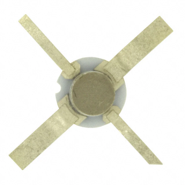
200 mil BeO Package
�AT-64020 Absolute Maximum Ratings
Symbol VEBO VCBO VCEO IC PT Tj TSTG Parameter Emitter-Base Voltage Collector-Base Voltage Collector-Emitter Voltage Collector Current Power Dissipation [�,3] Junction Temperature Storage Temperature Units V V V mA W °C °C Absolute Maximum[1] � 40 �0 �00 3 �00 -65 to �00 Thermal Resistance [2,4]: θjc = 40°C/W
Notes: 1. Permanent damage may occur if any of these limits are exceeded. 2. Tcase = 25°C. 3. Derate at 25 mW/°C for Tc > 80°C. 4. The small spot size of this technique results in a higher, though more accurate determination of θjc than do alternate methods. See MEASUREMENTS section “Thermal Resistance” for more information.
Electrical Specifications, TA = 25°C
Symbol |S �1E| � P1 dB G1 dB ηT hFE ICBO IEBO Parameters and Test Conditions[1] Insertion Power Gain; VCE = 16 V, IC = 110 mA Power Output @ 1 dB Gain Compression VCE = 16 V, IC = 110 mA 1 dB Compressed Gain; VCE = 16 V, IC = 110 mA Total Efficiency at 1 dB Compression: VCE = 16 V, IC = 110 mA Forward Current Transfer Ratio; VCE = 8 V, IC = 110 mA Collector Cutoff Current; VCB = 16 V Emitter Cutoff Current; VEB = 1 V f = �.0 GHz f = 4.0 GHz f = �.0 GHz f= 4.0 GHz f = �.0 GHz f = 4.0 GHz f = 4.0 GHz Units dB dBm dB % — µA µA �0 �6.5 8.5 Min. Typ. 7.0 �.0 �7.5 �6.5 10.0 6.5 35.0 50 �00 100 5.0 Max.
Note: 1. ηT = (RF Output Power)/(RF Input Power + VCEIC).
�
�AT-64020 Typical Performance, TA = 25°C
30 29 P1 dB (dBm) 28 27 26 25 1.0 15 30 25 POWER OUT (dBm) 12 G1 dB (dB) 20
ηT POUT
40 30 20 10 0 EFFICIENCY (%)
9
15 10 5 0
150 mA 110 mA 70 mA
6
150 mA 110 mA 70 mA
2.0
3.0
4.0
3 1.0
2.0
3.0
4.0
0
5
10
15
20
25
FREQUENCY (GHz)
FREQUENCY (GHz)
POWER IN (dBm)
Figure 1. Power Output @ 1 dB Gain Compression vs. Frequency and Collector Current. VCE = 16 V.
Figure 2. 1 dB Compressed Gain vs. Frequency and Collector Current. VCE = 16 V.
Figure 3. Output Power and E ciency vs. Input Power. VCE = 16 V, IC = 110 mA, f = 4.0 GHz.
35 30 25 GAIN (dB) 20 15 10 5 0 0.1 0.3 0.5 1.0 3.0 5.0
|S21E|2 MAG MSG MSG
FREQUENCY (GHz)
Figure 4. Insertion Power Gain, Maximum Available Gain and Maximum Stable Gain vs. Frequency. VCE = 16 V, IC = 110 mA.
Typical Scattering Parameters, Common Emitter, ZO = 50 Ω, TA = �5°C, VCE = 16 V, IC = 110 mA
Freq. GHz 0.1 0.5 1.0 1.5 �.0 �.5 3.0 3.5 4.0 4.5 5.0 Mag. .61 .75 .75 .74 .74 .73 .73 .74 .73 .7� .71 S11 Ang. -116 -173 171 159 148 141 130 119 107 93 79 dB 30.0 18.4 1�.5 9.� 7.0 5.� 3.8 �.7 1.8 0.9 0.1 S21 Mag. 31.51 8.�7 4.�3 �.90 �.�3 1.8� 1.56 1.37 1.�3 1.11 1.01 Ang. 130 86 66 50 35 �6 1� -� -16 -30 -43 dB -33.1 -�8.8 -�7.4 -�3.5 -�1.6 -19.8 -17.5 -16.1 -14.7 -13.3 -11.8 S12 Mag. .0�� .036 .043 .067 .083 .103 .133 .157 .186 .�17 .�56 Ang. 57 41 49 48 46 47 41 35 �6 18 8 Mag. .67 .�3 .�0 .�1 .�5 .�7 .3� .35 .38 .41 .4� S22 Ang. -48 -88 -100 -110 -1�0 -1�7 -135 -146 -158 -168 179
A model for this device is available in the DEVICE MODELS section.
3
�Ordering Information
Part Number AT-640�0 No. of Devices 100
200 mil BeO Package Dimensions
4 .300 ± .025 7.62 ± .64 45° 1 BASE NO REFERENCE EMITTER .060 1.52 .048 ± .010 1.21 ± .25 2 3 COLLECTOR Notes: (unless otherwise specified) 1. Dimensions are in mm 2. Tolerances in .xxx = ± 0.005 mm .xx = ± 0.13 3. Base of package is electrically isolated. .004 ± .002 .10 ± .05 EMITTER .030 .76
.128 3.25
.205 5.21
.023 .57
For product information and a complete list of distributors, please go to our web site:
www.avagotech.com
Avago, Avago Technologies, and the A logo are trademarks of Avago Technologies, Limited in the United States and other countries. Data subject to change. Copyright © �008 Avago Technologies Limited. All rights reserved. Obsoletes 5989-�657EN AV0�-1��0EN May 5, �008
�
很抱歉,暂时无法提供与“AT-64020”相匹配的价格&库存,您可以联系我们找货
免费人工找货