ATF-541M4
Low Noise Enhancement Mode Pseudomorphic HEMT
in a Miniature Leadless Package
Data Sheet
Description
Avago Technologies’ ATF‑541M4 is a high linearity, low
noise, single supply E‑PHEMT housed in a miniature lead‑
less package.
The ATF-541M4’s small size and low profile makes it ideal
for the design of hybrid module and other space-con‑
straint devices.
The device can be used in applications such as TMA and
front end LNA for Cellular/PCS and WCDMA base stations,
LNA and driver amplifiers for Wireless Data and 802.11b
WLAN.
Features
• High linearity performance
• Single Supply Enhancement Mode Technology[1]
• Very low noise figure
• Excellent uniformity in product specifications
• 800 micron gate width
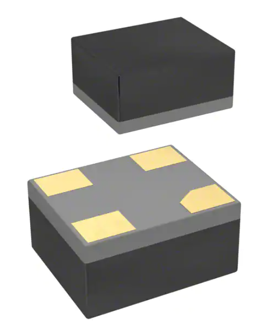
• Miniature leadless package
1.4 mm x 1.2 mm x 0.7 mm
• Tape-and-Reel packaging option available
Specifications
2 GHz; 3V, 60 mA (Typ.)
In addition, the device’s superior RF performance at higher
frequency makes it an ideal candidate for high frequency
applications such as WLL, 802.11a WLAN, 5–6 GHz UNII
and HIPERLAN applications.
• 35.8 dBm output 3rd order intercept
MiniPak 1.4 mm x 1.2 mm Package
• 17.5 dB associated gain
Rx
Pin Connections and Package Marking
Source
Pin 3
Gate
Pin 2
Rx
Drain
Pin 4
Source
Pin 1
Note:
Top View. Package marking provides orientation, product identifica‑
tion and date code.
“R” = Device Type Code
“x” = Date code character. A different character is assigned for each
month and year.
• 21.4 dBm output power at 1 dB gain compression
• 0.5 dB noise figure
Applications
• Low Noise Amplifier and Driver Amplifier for Cellular/
PCS and WCDMA Base Stations
• LNA and Driver Amplifier for WLAN, WLL/RLL and
MMDS applications
• General purpose discrete E-PHEMT for ultra low noise
applications in the 450 MHz to 10 GHz frequency range
Note:
1. Enhancement mode technology requires positive Vgs, thereby
eliminating the need for the negative gate voltage associated with
conventional depletion mode devices.
�ATF-541M4 Absolute Maximum Ratings [1]
Symbol
Parameter
Units
Absolute
Maximum
VDS
Drain-Source Voltage [2]
V
5
VGS
Gate-Source Voltage
V -5 to +1
VGD
Gate Drain Voltage [2]
V
5
IDS
Drain Current[2]
mA
120
IGS
Gate Current
mA
2
P
Total Power Dissipation
mW
360
Pin max.
RF Input Power
dBm
20
TCH
Channel Temperature
°C
150
TSTG
Storage Temperature
°C -65 to 150
θjc
Thermal Resistance
°C/W
[2]
[5]
diss
[3]
[5]
[4]
120
Notes:
1. Operation of this device above any one of
these parameters may cause permanent
damage.
2. Assumes DC quiescent conditions.
3. Source lead temperature is 25°C. Derate
4.7 mW/°C for TL > 74°C.
4. Thermal resistance measured using
150°C Liquid Crystal Measurement
method.
5. The device can handle +20 dBm RF Input
Power provided IGS is limited to 2 mA. IGS at
P1dB drive level is bias circuit dependent. See
applications section for additional informa‑
tion.
212
0.7V
100
0.6V
IDS (mA)
80
60
0.5V
40
20
0
0.4V
0.3V
0
1
2
3
4
VDS (V)
5
6
7
Figure 1. Typical I-V Curves.
(VGS = 0.1 V per step)
Product Consistency Distribution Charts [6, 7]
320
Cpk = 0.85
Stdev = 1.14
320
300
Cpk = 1.16
Stdev = 0.30
Cpk = 1.72
Stdev = 0.072
250
240
240
200
-3 Std
160
160
80
80
-3 Std
+3 Std
+3 Std
150
100
50
0
0
29
32
35
38
OIP3 (dBm)
Figure 2. OIP3 @ 2 GHz, 3 V, 60 mA.
LSL = 33.0, Nominal = 35.82
41
15
16
17
18
GAIN (dB)
19
Figure 3. Gain @ 2 GHz, 3 V, 60 mA.
LSL = 15.5, Nominal = 17.5, USL = 18.5
20
0
0.3
0.5
0.7
0.9
1.1
NF (dB)
Figure 4. NF @ 2 GHz, 3 V, 60 mA.
Nominal = 0.5, USL = 0.9
Notes:
6. Distribution data sample size is 500 samples taken from 6 different wafers. Future wafers allocated to this product may have nominal values
anywhere between the upper and lower limits.
7. Measurements made on production test board. This circuit represents a trade-off between an optimal noise match and a realizeable match
based on production test equipment. Circuit losses have been de-embedded from actual measurements.
�
�ATF-541M4 Electrical Specifications
TA = 25°C, RF parameters measured in a test circuit for a typical device
Symbol
Parameter and Test Condition
Units
Min.
Typ.
Max.
Vgs
Operational Gate Voltage
Vds = 3V, Ids = 60 mA
V
0.4
0.58
0.75
Threshold Voltage
Vds = 3V, Ids = 4 mA
V
0.18
0.36
0.52
Saturated Drain Current
Vth
Idss
Vds = 3V, Vgs = 0V
µA
—
0.28
5
Gm
Transconductance
Vds = 3V, gm = ∆Idss/∆Vgs;
∆Vgs = 0.75 – 0.7 = 0.05V
mmho
230
398
560
Igss
Vgd = Vgs = -3V
µA
—
—
200
NF
Noise Figure [1]
f = 2 GHz
Gate Leakage Current
Vds = 3V, Ids = 60 mA
Vds = 4V, Ids = 60 mA
dB
dB
—
—
0.5
0.5
0.9
—
Gain
Gain[1]
f = 2 GHz
Vds = 3V, Ids = 60 mA
Vds = 4V, Ids = 60 mA
dB
dB
15.5
—
17.5
18.1
18.5
—
OIP3
Output 3rd Order
f = 2 GHz
Intercept Point[1]
Vds = 3V, Ids = 60 mA
Vds = 4V, Ids = 60 mA
dBm
dBm
33
—
35.8
35.9
—
—
P1dB
1dB Compressed
Output Power[1]
Vds = 3V, Ids = 60 mA
Vds = 4V, Ids = 60 mA
dBm
dBm
—
—
21.4
22.1
—
—
f = 2 GHz
Notes:
1. Measurements obtained using production test board described in Figure 5.
Input
50 Ohm
Transmission
Line Including
Gate Bias T
(0.3 dB loss)
Input
Matching Circuit
Γ_mag = 0.11
Γ_ang = 141
(0.5 dB loss)
DUT
Output
Matching Circuit
Γ_mag = 0.314
Γ_ang = -167
(0.5 dB loss)
50 Ohm
Transmission
Line Including
Drain Bias T
(0.3 dB loss)
Output
Figure 5. Block diagram of 2 GHz production test board used for Noise Figure, Gain, P1dB, OIP3, and OIP3 measurements. This circuit represents a trade-off between an optimal noise match, maximum OIP3 match and associated impedance matching circuit losses. Circuit losses have been de-embedded from actual measurements.
Symbol
Parameter and Test Condition
Units
Min.
Typ.
Max.
Fmin
Minimum Noise Figure f = 900 GHz
f = 2 GHz
f = 3.9 GHz
f = 5.8 GHz
Vds = 3V, Ids = 60 mA
Vds = 3V, Ids = 60 mA
Vds = 3V, Ids = 60 mA
Vds = 3V, Ids = 60 mA
dB
dB
dB
dB
—
—
—
—
0.16
0.46
0.8
1.17
—
—
—
—
Ga
Associated Gain[2]
f = 900 GHz
f = 2 GHz
f = 3.9 GHz
f = 5.8 GHz
Vds = 3V, Ids = 60 mA
Vds = 3V, Ids = 60 mA
Vds = 3V, Ids = 60 mA
Vds = 3V, Ids = 60 mA
dB
dB
dB
dB
—
—
—
—
22.4
18.7
14.5
11.9
—
—
—
—
OIP3
Output 3rd Order
f = 900 GHz
Intercept Point[3]
f = 3.9 GHz
f = 5.8 GHz
Vds = 3V, Ids = 60 mA
Vds = 4V, Ids = 60 mA
Vds = 3V, Ids = 60 mA
Vds = 3V, Ids = 60 mA
dBm
dBm
dB
dB
—
—
—
—
35
35.1
36.6
37.6
—
—
—
—
P1dB
1dB Compressed
Output Power[3]
Vds = 3V, Ids = 60 mA
Vds = 4V, Ids = 60 mA
Vds = 3V, Ids = 60 mA
Vds = 3V, Ids = 60 mA
dBm
dBm
dB
dB
—
—
—
—
19.5
20.8
20.4
19.4
—
—
—
—
[2]
f = 900 GHz
f = 3.9 GHz
f = 5.8 GHz
Notes:
2. Fmin and associated gain at minimum noise figure (Ga) values are based on a set of 16 noise figure measurements made at 16 different im‑
pedances using an ATN NP5 test system. From these measurements a true Fmin and Ga is calculated. Refer to the noise parameter application
section for more information.
3. P1dB and OIP3 measurements made in an InterContinental Microwave (ICM) test fixture with double stub tuners and bias tees. The input was
tuned for minimum noise figure and the output was tuned for maximum OIP3.
�
�ATF-541M4 Typical Performance Curves
0.60
40
0.26
0.24
0.22
0.45
30
0.20
dB/dBm
0.50
Fmin (dB)
Fmin (dB)
0.55
0.18
0.16
20
15
0.12
0
20
40
60
80
0.10
100
0
20
40
Id (mA)
30
25
20
20
40
0
20
40
60
80
100
Id (mA)
Figure 9. Gain, OIP3 & P1dB vs. Ids Tuned
for Max OIP3 and Min NF at 900 MHz,
Vds = 3V[3].
80
100
Figure 8. Gain, OIP3 & P1dB vs. Ids Tuned
for Max OIP3 and Min NF at 2 GHz,
Vds = 3V[2].
2.5
30
2.0
25
1.5
20
1.0
0
60
Ids (mA)
40 mA
60 mA
80 mA
15
80 mA
60 mA
40 mA
0.5
0
10
100
Ga (dB)
Gain
OIP3
P1dB
Fmin (dB)
dB/dBm
80
Figure 7. Fmin vs. Ids at 900 MHz, Vds = 3V[1]
40
35
60
Id (mA)
Figure 6. Fmin vs. Ids at 2 GHz, Vds = 3V[1]
15
25
0.14
0.40
0.35
Gain
OIP3
P1dB
35
0
2
4
6
8
10
FREQUENCY (GHz)
Figure 10. Fmin vs. Frequency vs. Ids,
Vds = 3V[1].
10
12
5
0
2
4
6
8
10
12
FREQUENCY (GHz)
Figure 11. Ga vs. Frequency vs. Ids,
Vds = 3V[1].
Notes:
1. Fmin and associated gain at minimum noise figure (Ga) values are based on a set of 16 noise figure measurements made at 16 different im‑
pedances using an ATN NP5 test system. From these measurements a true Fmin and Ga is calculated. Refer to the noise parameter application
section for more information.
2. Measurements obtained using production test board described in Figure 5.
3. Input tuned for minimum NF and the output tuned for maximum OIP3 using an InterContinental Microwave (ICM) test fixture, double stub
tuners and bias tees.
�
�ATF-541M4 Typical Performance Curves, continued
30
45
25 C
-40 C
85 C
1.5
15
10
NF (dB)
35
20
30
25
25 C
-40 C
85 C
20
5
0
0
1
2
3
4
5
6
10
7
0
1
2
25 C
-40 C
85 C
22
21
20
19
18
0
1
2
3
4
3
4
5
6
7
Figure 13. OIP3 vs. Freq. and Temperature
Tuned for Max OIP3 and Min NF at
Vds = 3V, Ids = 60 mA[1].
23
P1dB (dBm)
0.5
FREQUENCY (GHz)
Figure 12. Gain vs. Freq. and Temperature
Tuned for Max OIP3 and Min NF at
Vds = 3V, Ids = 60 mA[1].
5
6
7
FREQUENCY (GHz)
Figure 15. P1dB vs. Freq. and Temperature
Tuned for Max OIP3 and Min NF at
Vds = 3V, Ids = 60 mA[1].
ATF-541M4 Output Reflection Coefficient Parameters Tuned
for Maximum Output IP3[1]; VDS = 3V, IDS = 60 mA
Freq
(GHz)
Gamma[2]
Out_Mag.
(Mag)
0.9
2.0
3.9
5.8
0.006
23
0.314 -167
0.321
134
0.027
89
Gamma[2]
Out_Mag.
(Degrees)
OIP3
P1dB
(dBm)
(dBm)
35.04
35.82
36.60
37.62
19.47
21.36
20.37
19.38
Notes:
1. Input tuned for minimum NF and the output tuned for maximum
OIP3 using an InterContinental Microwave (ICM) test fixture, double
stub tuners and bias tees.
2. Gamma out is the reflection coefficient of the matching circuit pre‑
sented to the output of the device.
�
1.0
15
FREQUENCY (GHz)
17
25 C
-40 C
85 C
40
OIP3 (dBm)
GAIN (dB)
25
2.0
0
0
1
2
3
4
5
6
FREQUENCY (GHz)
Figure 14. NF vs. Freq. and Temperature
Tuned for Max OIP3 and Min NF at
Vds = 3V, Ids = 60 mA[1].
7
�ATF-541M4 Typical Scattering Parameters, VDS = 3V, IDS = 40 mA
Freq. S11
S21
GHz
Mag.
Ang.
dB
Mag.
Ang.
S12
Mag.
Ang.
S22
Mag.
Ang.
MSG/MAG
dB
0.1
0.5
0.9
1.0
1.5
1.9
2.0
2.5
3.0
4.0
5.0
6.0
7.0
8.0
9.0
10.0
11.0
12.0
13.0
14.0
15.0
16.0
17.0
18.0
0.01
80.2
0.03
54.4
0.04
41.2
0.04
39.0
0.05
32.8
0.05
30.4
0.05
30.6
0.06
29.7
0.06
29.5
0.07
29.3
0.07
27.9
0.09
25.1
0.10
22.3
0.11
19.0
0.12
15.1
0.13
10.5
0.14
4.8
0.15 -1.7
0.16 -8.5
0.16 -15.9
0.17 -24.1
0.17 -31.6
0.17 -39.0
0.17 -45.9
0.58 -10.6
0.46 -45.3
0.34 -66.5
0.32 -71.0
0.23 -87.8
0.19 -97.9
0.16 -101.6
0.13 -113.1
0.11 -128.4
0.11 -152.9
0.11 -174.7
0.12
173.9
0.13
157.8
0.14
145.8
0.16
135.6
0.19
124.6
0.22
113.5
0.27
102.7
0.32
92.5
0.37
83.1
0.44
74.2
0.50
66.0
0.57
60.5
0.62
55.9
33.81
27.98
25.36
25.01
22.64
21.75
21.48
19.82
19.06
15.14
12.85
11.68
10.34
9.24
8.31
7.74
7.01
6.58
6.19
5.73
5.46
4.53
4.93
4.44
24.03
169.5
18.85
135.7
13.74
115.0
12.69
110.9
9.18
96.1
7.48
87.7
7.03
86.4
5.75
78.3
4.83
71.1
3.67
58.3
2.96
46.6
2.52
34.5
2.16
23.9
1.89
13.6
1.68
3.6
1.52 -6.5
1.38 -16.9
1.26 -27.5
1.15 -37.6
1.04 -48.8
0.94 -59.4
0.82 -69.3
0.74 -78.2
0.65 -86.9
Typical Noise Parameters, VDS = 3V, IDS = 40 mA
Freq
Fmin
Γopt
Γopt
Rn/50
GHz
dB
Mag.
Ang.
Ga
dB
0.5
0.9
1.0
1.9
2.0
2.4
3.0
3.9
5.0
5.8
6.0
7.0
8.0
9.0
10.0
26.17
22.19
21.81
18.72
18.24
17.16
15.91
14.26
12.74
11.72
10.32
9.77
9.46
8.64
8.15
0.10
0.12
0.17
0.40
0.41
0.51
0.55
0.64
0.95
1.07
1.10
1.30
1.45
1.57
1.69
0.45
8.3
0.41
11.3
0.29
23.8
0.23
89.2
0.22
89.9
0.24
112.1
0.29
140.2
0.34
165.4
0.35 -173.4
0.34 -160.3
0.40 -151.2
0.42 -139.3
0.48 -129.2
0.55 -118.0
0.59 -101.7
0.06
0.06
0.05
0.05
0.05
0.05
0.05
0.04
0.04
0.05
0.08
0.10
0.13
0.21
0.34
40
35
MSG/MAG and |S21|2 (dB)
0.99 -16.4
27.62
0.88 -71.2
25.51
0.79 -107.2
22.76
0.77 -114.0
22.07
0.73 -137.2
19.26
0.71 -150.1
17.48
0.70 -155.1
16.94
0.69 -168.4
15.19
0.69 -178.1
13.68
0.69
166.9
11.30
0.70
155.0
9.44
0.71
139.7
8.02
0.72
129.2
6.67
0.73
119.3
5.54
0.74
110.0
4.51
0.76
100.3
3.61
0.77
90.5
2.80
0.79
82.1
2.01
0.81
72.4
1.21
0.83
62.2
0.37
0.85
52.3 -0.51
0.86
42.7 -1.70
0.89
33.1 -2.59
0.90
24.5 -3.81
MSG
30
25
20
15
MAG
10
|S21|2
5
0
-5
-10
0
5
10
15
20
FREQUENCY (GHz)
Figure 16. MSG/MAG and |S21|2 vs.
Frequency at 3V, 40 mA.
Notes:
1. The Fmin values are based on a set of 16 noise figure measurements made at 16 different impedances using an ATN NP5 test system. From
these measurements a true Fmin is calculated. Refer to the noise parameter application section for more information.
2. Refer to the applications section for additional information on the test fixture used for the measurement of the s and noise parameters.
�
�ATF-541M4 Typical Scattering Parameters, VDS = 3V, IDS = 60 mA
Freq. S11
S21
GHz
Mag.
Ang.
dB
Mag.
Ang.
S12
Mag.
Ang.
S22
Mag.
Ang.
MSG/MAG
dB
0.1
0.5
0.9
1.0
1.5
1.9
2.0
2.5
3.0
4.0
5.0
6.0
7.0
8.0
9.0
10.0
11.0
12.0
13.0
14.0
15.0
16.0
17.0
18.0
0.01
85.1
0.03
54.2
0.04
41.8
0.04
40.2
0.05
34.6
0.05
32.8
0.05
33.5
0.05
34.1
0.06
33.4
0.07
32.8
0.08
32.0
0.09
28.2
0.10
25.1
0.11
21.1
0.12
16.6
0.13
11.2
0.14
5.5
0.15 -1.1
0.16 -8.7
0.17 -15.6
0.17 -23.4
0.17 -31.6
0.17 -38.7
0.17 -45.8
0.54 -11.3
0.41 -48.1
0.30 -70.1
0.28 -74.9
0.20 -92.5
0.17 -103.3
0.14 -108.9
0.12 -122.4
0.10 -138.7
0.10 -164.1
0.09
174.9
0.11
162.9
0.12
149.1
0.14
138.7
0.17
129.5
0.19
119.3
0.23
108.8
0.27
98.6
0.32
89.2
0.38
80.3
0.44
71.7
0.49
64.3
0.57
58.8
0.62
54.7
34.18
28.25
25.54
25.19
22.78
21.88
21.61
20.73
19.17
15.26
13.21
11.80
10.30
9.42
8.46
7.86
7.21
6.73
6.11
5.98
5.54
4.75
5.73
4.51
26.18
168.9
20.03
133.9
14.34
113.5
13.22
109.4
9.49
95.1
7.70
86.9
7.24
85.7
5.92
77.9
4.96
70.8
3.77
58.3
3.04
46.8
2.58
34.8
2.21
24.4
1.94
14.3
1.72
4.4
1.55 -5.7
1.42 -16.0
1.29 -26.3
1.18 -36.3
1.07 -47.4
0.96 -58.1
0.85 -67.9
0.76 -76.8
0.67 -84.8
Typical Noise Parameters, VDS = 3V, IDS = 60 mA
Freq
Fmin
Γopt
Γopt
Rn/50
GHz
dB
Mag.
Ang.
Ga
dB
0.5
0.9
1.0
1.9
2.0
2.4
3.0
3.9
5.0
5.8
6.0
7.0
8.0
9.0
10.0
27.06
22.88
22.44
19.17
18.69
17.57
16.26
14.54
12.97
11.85
10.98
10.03
9.66
8.82
8.32
0.12
0.16
0.19
0.45
0.46
0.57
0.62
0.80
1.02
1.17
1.22
1.41
1.49
1.69
1.87
0.37
13.2
0.34
10.9
0.21
30.8
0.22
102.9
0.21
104.2
0.23
125.2
0.30
149.0
0.35
173.1
0.43 -168.3
0.46 -155.8
0.51 -146.4
0.52 -137.0
0.54 -129.5
0.56 -115.1
0.61 -99.8
0.05
0.06
0.04
0.05
0.05
0.05
0.04
0.04
0.05
0.06
0.09
0.11
0.15
0.25
0.40
40
35
MSG/MAG and |S21|2 (dB)
0.99 -17.6
28.36
0.87 -74.7
26.04
0.78 -110.7
23.13
0.76 -117.6
22.42
0.72 -140.1
19.54
0.70 -152.6
17.73
0.70 -157.5
17.19
0.69 -170.4
15.45
0.69 -179.9
13.91
0.69
165.7
11.53
0.70
153.8
9.66
0.71
138.8
8.25
0.71
128.6
6.89
0.73
118.6
5.76
0.74
109.2
4.72
0.76
99.9
3.80
0.77
89.7
3.03
0.79
81.5
2.23
0.80
71.8
1.45
0.83
61.7
0.58
0.85
52.2 -0.31
0.86
42.1 -1.41
0.90
33.2 -2.34
0.90
24.3 -3.53
MSG
30
25
20
15
MAG
10
|S21|2
5
0
-5
-10
0
5
10
15
20
FREQUENCY (GHz)
Figure 17. MSG/MAG and |S21|2 vs.
Frequency at 3V, 60 mA.
Notes:
1. The Fmin values are based on a set of 16 noise figure measurements made at 16 different impedances using an ATN NP5 test system. From
these measurements a true Fmin is calculated. Refer to the noise parameter application section for more information.
2. Refer to the applications section for additional information on the test fixture used for the measurement of the s and noise parameters.
�
�ATF-541M4 Typical Scattering Parameters, VDS = 3V, IDS = 80 mA
Freq. S11
S21
GHz
Mag.
Ang.
dB
Mag.
Ang.
S12
Mag.
Ang.
S22
Mag.
Ang.
MSG/MAG
dB
0.1
0.5
0.9
1.0
1.5
1.9
2.0
2.5
3.0
4.0
5.0
6.0
7.0
8.0
9.0
10.0
11.0
12.0
13.0
14.0
15.0
16.0
17.0
18.0
0.01
79.8
0.03
54.7
0.04
43.1
0.04
41.5
0.04
36.3
0.05
34.8
0.05
35.8
0.05
36.0
0.06
35.8
0.06
35.0
0.07
33.7
0.09
29.6
0.10
26.6
0.11
22.3
0.12
17.8
0.13
12.1
0.14
6.1
0.15 -0.4
0.16 -7.8
0.17 -15.0
0.17 -23.3
0.17 -31.0
0.17 -39.1
0.17 -45.5
0.50 -11.6
0.39 -49.1
0.28 -71.5
0.26 -76.4
0.19 -94.6
0.16 -105.8
0.13 -112.9
0.11 -127.2
0.10 -144.2
0.10 -170.0
0.10
168.7
0.11
156.1
0.12
143.5
0.14
133.6
0.17
125.1
0.19
115.7
0.23
105.6
0.27
95.7
0.32
86.7
0.37
78.3
0.44
70.0
0.49
63.1
0.57
57.7
0.62
53.6
34.30
28.33
25.61
25.26
23.80
21.93
21.66
20.78
19.22
14.97
13.05
11.67
10.52
9.47
8.52
7.88
7.03
6.75
6.21
6.12
5.66
4.89
5.21
4.07
26.94
168.8
20.44
133.6
14.57
113.2
13.42
109.1
9.60
95.0
7.79
86.9
7.33
85.8
5.98
78.0
5.01
71.0
3.81
58.5
3.07
47.2
2.61
35.3
2.23
25.0
1.96
14.8
1.74
5.2
1.56 -4.9
1.43 -15.1
1.30 -25.2
1.20 -35.3
1.09 -46.6
0.98 -56.2
0.87 -67.1
0.78 -75.9
0.68 -83.6
Typical Noise Parameters, VDS = 3V, IDS = 80 mA
Freq
Fmin
Γopt
Γopt
Rn/50
GHz
dB
Mag.
Ang.
Ga
dB
0.5
0.9
1.0
1.9
2.0
2.4
3.0
3.9
5.0
5.8
6.0
7.0
8.0
9.0
10.0
27.83
23.58
23.43
19.57
19.13
18.05
16.60
14.81
13.21
12.20
11.35
10.24
9.84
9.00
8.46
0.21
0.25
0.28
0.53
0.56
0.64
0.72
0.81
1.03
1.33
1.40
1.59
1.79
2.01
2.20
0.23
24.4
0.20
17.8
0.11
60.8
0.21
121.1
0.20
124.5
0.26
142.6
0.32
159.7
0.38
179.2
0.41 -153.7
0.42 -152.5
0.46 -143.4
0.47 -139.1
0.53 -127.3
0.59 -113.4
0.63 -97.9
0.05
0.06
0.04
0.05
0.05
0.05
0.05
0.05
0.05
0.07
0.10
0.13
0.19
0.31
0.5
40
35
MSG/MAG and |S21|2 (dB)
0.97 -17.9
28.61
0.85 -76.2
26.21
0.77 -112.1
23.27
0.75 -119.2
22.55
0.71 -142.2
19.65
0.70 -154.9
17.83
0.69 -159.5
17.30
0.69 -171.1
15.53
0.69
179.5
14.00
0.69
165.2
11.62
0.70
153.3
9.75
0.70
138.3
8.33
0.72
127.8
6.97
0.73
118.0
5.84
0.74
109.1
4.82
0.76
99.3
3.89
0.76
89.7
3.11
0.79
80.9
2.29
0.80
71.9
1.56
0.83
61.8
0.73
0.85
52.1 -0.18
0.86
41.6 -1.22
0.89
32.9 -2.18
0.89
24.3 -3.36
MSG
30
25
20
15
MAG
10
|S21|2
5
0
-5
-10
0
5
10
15
20
FREQUENCY (GHz)
Figure 18. MSG/MAG and |S21|2 vs.
Frequency at 3V, 80 mA.
Notes:
1. The Fmin values are based on a set of 16 noise figure measurements made at 16 different impedances using an ATN NP5 test system. From
these measurements a true Fmin is calculated. Refer to the noise parameter application section for more information.
2. Refer to the applications section for additional information on the test fixture used for the measurement of the s and noise parameters.
�
�ATF-541M4 Typical Scattering Parameters, VDS = 4V, IDS = 60 mA
Freq. S11
S21
GHz
Mag.
Ang.
dB
Mag.
Ang.
S12
Mag.
Ang.
S22
Mag.
Ang.
MSG/MAG
dB
0.1
0.5
0.9
1.0
1.5
1.9
2.0
2.5
3.0
4.0
5.0
6.0
7.0
8.0
9.0
10.0
11.0
12.0
13.0
14.0
15.0
16.0
17.0
18.0
0.01
81.0
0.03
54.5
0.04
41.6
0.04
39.4
0.04
35.2
0.05
33.3
0.05
33.7
0.051
34.2
0.05
33.1
0.06
33.2
0.07
32.4
0.08
29.5
0.09
26.4
0.10
22.7
0.11
18.2
0.13
13.4
0.14
7.2
0.15
0.6
0.16 -6.5
0.17 -13.9
0.17 -21.7
0.17 -29.9
0.18 -37.8
0.17 -44.8
0.56 -10.7
0.44 -44.7
0.32 -64.3
0.29 -68.3
0.21 -82.7
0.18 -91.2
0.14 -93.8
0.11 -103.7
0.10 -117.7
0.09 -141.7
0.09 -166.9
0.10 -175.8
0.12
163.3
0.13
149.1
0.14
138.2
0.17
126.7
0.20
114.9
0.24
103.7
0.29
93.3
0.35
84.3
0.42
75.0
0.48
67.0
0.55
61.1
0.61
56.4
34.19
28.27
25.57
25.21
23.78
21.90
21.64
20.68
17.98
15.13
13.17
11.68
10.53
9.44
8.76
8.01
7.30
6.91
6.54
6.22
5.73
5.20
6.31
5.96
26.27
168.9
20.12
133.9
14.42
113.6
13.29
109.4
9.55
95.1
7.75
86.9
7.29
85.6
5.96
77.7
5.00
70.6
3.80
57.9
3.06
46.4
2.60
34.4
2.23
23.9
1.95
13.5
1.74
3.6
1.56 -6.6
1.42 -17.1
1.30 -27.6
1.19 -37.8
1.08 -48.9
0.97 -59.6
0.85 -69.7
0.77 -78.7
0.67 -87.4
Typical Noise Parameters, VDS = 4V, IDS = 60 mA
Freq
Fmin
Γopt
Γopt
Rn/50
GHz
dB
Mag.
Ang.
Ga
dB
0.5
0.9
1.0
1.9
2.0
2.4
3.0
3.9
5.0
5.8
6.0
7.0
8.0
9.0
10.0
27.18
22.95
22.51
19.14
18.66
17.61
16.26
14.58
13.04
12.01
11.05
10.11
9.76
8.95
8.44
0.13
0.16
0.20
0.45
0.47
0.57
0.63
0.73
1.05
1.21
1.23
1.43
1.61
1.80
2.01
0.36
14.2
0.35
13.3
0.22
33.7
0.22
101.6
0.20
102.7
0.24
126.0
0.29
148.9
0.35
172.3
0.37 -168.4
0.38 -155.9
0.41 -151.0
0.45 -139.9
0.51 -129.9
0.57 -114.8
0.61 -99.2
0.05
0.06
0.05
0.05
0.06
0.05
0.05
0.04
0.05
0.06
0.08
0.11
0.15
0.26
0.41
40
35
MSG/MAG and |S21|2 (dB)
0.99 -17.5
28.39
0.87 -74.8
26.07
0.78 -110.7
23.18
0.76 -117.5
22.47
0.72 -141.4
19.60
0.70 -154.3
17.79
0.69 -159.0
17.25
0.69 -170.1
15.50
0.69 -179.6
13.98
0.69
165.9
11.60
0.70
153.9
9.72
0.70
138.8
8.31
0.72
128.6
6.96
0.73
118.8
5.82
0.75
109.5
4.80
0.76
99.9
3.89
0.77
90.1
3.07
0.79
81.5
2.27
0.81
71.6
1.47
0.83
62.2
0.68
0.85
51.9 -0.28
0.87
42.1 -1.39
0.90
32.7 -2.28
0.90
24.2 -3.52
MSG
30
25
20
MAG
15
10
|S21|
5
2
0
-5
-10
0
5
10
15
20
FREQUENCY (GHz)
Figure 19. MSG/MAG and |S21|2 vs.
Frequency at 4V, 60 mA.
Notes:
1. The Fmin values are based on a set of 16 noise figure measurements made at 16 different impedances using an ATN NP5 test system. From
these measurements a true Fmin is calculated. Refer to the noise parameter application section for more information.
2. Refer to the applications section for additional information on the test fixture used for the measurement of the s and noise parameters.
�
�S and Noise Parameter Measurements
The position of the reference planes
used for the measurement of both S
and Noise Parameter measurements
is shown in Figure 20. The reference
plane can be described as being at
the center of both the gate and drain
pads.
S and noise parameters are measured
with a 50 ohm microstrip test fixture
made with a 0.010" thickness alu‑
minum substrate. Both source leads
are connected directly to ground via
a 0.010" thickness metal rib which
provides a very low inductance path
to ground for both source leads. The
inductance associated with the ad‑
dition of printed circuit board plated
through holes and source bypass
capacitors must be added to the
computer circuit simulation to prop‑
erly model the effect of grounding
the source leads in a typical amplifier
design.
Reference
Plane
Source
Pin 3
Drain
Pin 4
Sx
Source
Pin 1
Gate
Pin 2
Microstrip
Transmission Lines
Figure 20.
Noise Parameter Applications Information
The Fmin values are based on a set
of 16 noise figure measurements
made at 16 different impedances
using an ATN NP5 test system. From
these measurements, a true Fmin is
calculated. Fmin represents the true
minimum noise figure of the device
when the device is presented with an
impedance matching network that
transforms the source impedance,
typically 50Ω, to an impedance repre‑
sented by the reflection coefficient Γo.
The designer must design a matching
network that will present Γo to the
device with minimal associated circuit
losses. The noise figure of the com‑
10
pleted amplifier is equal to the noise
figure of the device plus the losses of
the matching network preceding the
device. The noise figure of the device
is equal to Fmin only when the device
is presented with Γo. If the reflection
coefficient of the matching network is
other than Γo, then the noise figure of
the device will be greater than Fmin
based on the following equation.
NF = Fmin + 4 Rn
|Γs – Γo | 2
Zo (|1 + Γo| 2)(1 - |Γs| 2)
Where Rn/Zo is the normalized noise
resistance, Γo is the optimum reflec‑
tion coefficient required to produce
Fmin and Γs is the reflection coeffi‑
cient of the source impedance actu‑
ally presented to the device.
The losses of the matching networks
are non-zero and they will also add to
the noise figure of the device creating
a higher amplifier noise figure. The
losses of the matching networks are
related to the Q of the components
and associated printed circuit board
loss. Γo is typically fairly low at higher
frequencies and increases as fre‑
quency is lowered. Larger gate width
devices will typically have a lower Γo
as compared to narrower gate width
devices. Typically for FETs , the higher
Γo usually infers that an impedance
much higher than 50Ω is required for
the device to produce Fmin. At VHF
frequencies and even lower L Band
frequencies, the required imped‑
ance can be in the vicinity of several
thousand ohms. Matching to such a
high impedance requires very hi-Q
components in order to minimize cir‑
cuit losses. As an example at 900 MHz,
when airwwound coils (Q>100)are
used for matching networks, the loss
can still be up to 0.25 dB which will
add directly to the noise figure of the
device. Using muiltilayer molded in‑
ductors with Qs in the 30 to 50 range
results in additional loss over the air‑
wound coil. Losses as high as 0.5 dB
or greater add to the typical 0.15 dB
Fmin of the device creating an ampli‑
fier noise figure of nearly 0.65 dB.
SMT Assembly
The package can be soldered us‑
ing either lead-bearing or lead-free
alloys (higher peak temperatures).
Reliable assembly of surface mount
components is a complex process that
involves many material, process, and
equipment factors, including: method
of heating (e.g. IR or vapor phase
reflow, wave soldering, etc) circuit
board material, conductor thickness
and pattern, type of solder alloy, and
the thermal conductivity and thermal
mass of components. Components
with a low mass, such as the Minipak
1412 package, will reach solder reflow
temperatures faster than those with a
greater mass.
The recommended leaded solder
time-temperature profile is shown in
Figure 21. This profile is representative
of an IR reflow type of surface mount
assembly process. After ramping up
from room temperature, the circuit
board with components attached
to it (held in place with solder paste)
passes through one or more preheat
zones. The preheat zones increase the
temperature of the board and compo‑
nents to prevent thermal shock and
begin evaporating solvents from the
solder paste. The reflow zone briefly
elevates the temperature sufficiently
to produce a reflow of the solder.
The rates of change of temperature
for the ramp-up and cool-down zones
are chosen to be low enough to not
cause deformation of board or dam‑
age to components due to thermal
shock. The maximum temperature
in the reflow zone (Tmax) should not
exceed 235°C for leaded solder.
These parameters are typical for a
surface mount assembly process for
the ATF-541M4. As a general guide‑
line, the circuit board and compo‑
nents should only be exposed to the
minimum temperatures and times
the necessary to achieve a uniform
reflow of solder.
The recommended lead-free reflow
profile is shown in Figure 22.
�Electrostatic Sensitivity
FETs and RFICs are electrostatic dis‑
charge (ESD) sensitive devices. Avago
devices are manufactured using
a very robust and reliable PHEMT
process, however, permanent dam‑
age may occur to these devices if
they are subjected to high-energy
electrostatic discharges. Electrostatic
charges as high as several thousand
volts (which readily accumulate on the
human body and on test equipment)
can discharge without detection and
may result in failure or degradation in
performance and reliability.
Electronic devices may be subjected
to ESD damage in any of the follow‑
ing areas:
• Storage & handling
• Inspection
• Assembly & testing
• In-circuit use
The ATF-541M4 is an ESD Class 1
device. Therefore, proper ESD pre‑
cautions are recommended when
handling, inspecting, testing, and
assembling these devices to avoid
damage.
250
TMAX
Any user-accessible points in wireless
equipment (e.g. antenna or battery
terminals) provide an opportunity for
ESD damage.
For circuit applications in which the
ATF-541M4 is used as an input or
output stage with close coupling
to an external antenna, the device
should be protected from high volt‑
age spikes due to human contact with
the antenna. A good practice, illus‑
trated in Figure 23, is to place a shunt
inductor or RF choke at the antenna
connection to protect the receiver
and transmitter circuits. It is often ad‑
vantageous to integrate the RF choke
into the design of the diplexer or T/R
switch control circuitry.
TEMPERATURE ( C)
200
150
Reflow
Zone
100
Preheat
Zone
Cool Down
Zone
50
0
0
60
120
180
240
300
TIME (seconds)
Figure 21. Leaded Solder Reflow Profile.
350
Peak Temperature
Min. 240 C
Max. 255 C
TEMPERATURE ( C)
300
250
221
Reflow Time
Min. 60s
Max. 90s
200
150
100
Preheat 130 –170 C
Min. 60s
Max. 150s
50
0
0
30
60
90
120
150
180
210
TIME (seconds)
Figure 22. Lead-free Solder Reflow Profile.
11
240
270
300
330
360
Figure 23. In-circuit ESD Protection.
�ATF-541M4 Applications Information
Introduction
Avago Technologies’s ATF‑541M4 is a
low noise enhancement mode PHEMT
designed for use in low cost commer‑
cial applications in the VHF through 6
GHz frequency range. As opposed to a
typical depletion mode PHEMT where
the gate must be made negative with
respect to the source for proper opera‑
tion, an enhancement mode PHEMT
requires that the gate be made more
positive than the source for normal
operation. Therefore a negative power
supply voltage is not required for an
enhancement mode device. Biasing an
enhancement mode PHEMT is much
like biasing the typical bipolar junc‑
tion transistor. Instead of a 0.7V base
to emitter voltage, the ATF-541M4
enhancement mode PHEMT requires a
nominal 0.58V potential between the
gate and source for a nominal drain
current of 60 mA.
Matching Networks
The techniques for impedance match‑
ing an enhancement mode device are
very similar to those for matching a
depletion mode device. The only dif‑
ference is in the method of supplying
gate bias. S and Noise Parameters for
various bias conditions are listed in this
data sheet. The circuit shown in Figure
1 shows a typical LNA circuit normally
used for 900 and 1900 MHz applica‑
tions. (Consult the Avago Technologies
web site for application notes covering
specific designs and applications). High
pass impedance matching networks
consisting of L1/C1 and L4/C4 provide
the appropriate match for noise fig‑
ure, gain, S11 and S22. The high pass
structure also provides low frequency
gain reduction which can be beneficial
from the standpoint of improving outof-band rejection.
Capacitors C2 and C5 provide a low
impedance in-band RF bypass for
12
the matching networks. Resistors R3
and R4 provide a very important low
frequency termination for the device.
The resistive termination improves
low frequency stability. Capacitors
C3 and C6 provide the RF bypass
for resistors R3 and R4. Their value
should be chosen carefully as C3 and
C6 also provide a termination for low
frequency mixing products. These
mixing products are as a result of two
or more in-band signals mixing and
producing third order in-band distor‑
tion products. The low frequency or
difference mixing products are termi‑
nated by C3 and C6. For best suppres‑
sion of third order distortion products
based on the CDMA 1.25 MHz signal
spacing, C3 and C6 should be 0.1 uF
in value. Smaller values of capacitance
will not suppress the generation of
the 1.25 MHz difference signal and
as a result will show up as poorer two
tone IP3 results.
C4
C1
INPUT
Q1
Zo
L1
L2
R4
OUTPUT
Zo
L4
L3
C2
C5
R3
R5
R1
C3
C6
R2
Vdd
Figure 1. Typical ATF-541M4 LNA with Passive Biasing.
Bias Networks
One of the major advantages of the
enhancement mode technology is
that it allows the designer to be able
to dc ground the source leads and
then merely apply a positive voltage
on the gate to set the desired amount
of quiescent drain current Id.
Whereas a depletion mode PHEMT
pulls maximum drain current when
V gs = 0 V, an enhancement mode
PHEMT pulls only a small amount of
leakage current when Vgs= 0V. Only
when Vgs is increased above Vto, the
device threshold voltage, will drain
current start to flow. At a Vds of 3V and
a nominal Vgs of 0.58V, the drain cur‑
rent Id will be approximately 60 mA.
The data sheet suggests a minimum
and maximum Vgs over which the
desired amount of drain current will
be achieved. It is also important to
note that if the gate terminal is left
open circuited, the device will pull
some amount of drain current due
to leakage current creating a voltage
differential between the gate and
source terminals.
Passive Biasing
Passive biasing of the ATF-541M4 is
accomplished by the use of a volt‑
age divider consisting of R1 and R2
connected to the gate of the device.
The voltage for the divider is derived
from the drain voltage. This provides a
form of voltage feedback (through the
use of R3) to help keep drain current
constant. Resistor R5 (approximately
10KΩ) is added to limit the gate cur‑
rent of enhancement mode devices
such as the ATF‑541M4. This is espe‑
cially important when the device is
driven to P1dB or Psat.
Resistor R3 is calculated based on
desired Vds , Ids and available power
supply voltage.
R3 = VDD – Vds
(1)
Ids + IBB
VDD is the power supply voltage.
Vds is the device drain to source volt‑
age.
Ids is the desired drain current.
I BB is the current flowing through
the R1/R2 resistor voltage divider
network.
�The value of resistors R1 and R2 are
calculated with the following for‑
mulas
R1 = Vgs
(2)
IBB
R2 = (Vds – Vgs) R1
Vgs
(3)
Example Circuit
VDD = 5 V
Vds = 3V
Ids = 60 mA
Vgs = 0.58 V
R1 and R2 provide a constant voltage
source at the base of a PNP transistor
at Q2. The constant voltage at the base
of Q2 is raised by 0.7 volts at the emit‑
ter. The constant emitter voltage plus
the regulated VDD supply are present
across resistor R3. Constant voltage
across R3 provides a constant current
supply for the drain current. Resistors
R1 and R2 are used to set the desired
Vds. The combined series value of these
resistors also sets the amount of extra
current consumed by the bias net‑
work. The equations that describe the
circuit’s operation are as follows.
Choose I BB to be at least 10X the
maximum expected gate leakage
current. IBB was chosen to be 2 mA for
this example. Using equations (1), (2),
and (3) the resistors are calculated as
follows
R1 = 290Ω
R2 = 1210Ω
R3 = 32.3Ω
VE = Vds + (Ids • R4)
VB = VE – VBE
VB =
R1 VDD
R1 + R2
(3)
Active Bias
Active biasing provides a means of
keeping the quiescent bias point con‑
stant over temperature and constant
over lot to lot variations in device dc
performance. The advantage of the
active biasing of an enhancement
mode PHEMT versus a depletion
mode PHEMT is that a negative power
source is not required. The techniques
of active biasing an enhancement
mode device are very similar to
those used to bias a bipolar junction
transistor.
VDD = IBB (R1 + R2)
(5)
An active bias scheme is shown in
Figure 2.
Example Circuit
VDD = 5 V
Vds = 3V
Ids = 60 mA
R4 = 10Ω
VBE = 0.7 V
C4
C1
INPUT
Q1
Zo
L1
L2
R5
OUTPUT
Zo
L3
C2
L4
C5
R3 = VDD – VE
Ids
(1)
(2)
(4)
Rearranging equation (4)
provides the following formula
R2 = R1 (VDD – VB)
VB
(4A)
and rearranging equation (5)
provides the follow formula
R1 =
(
VDD
IBB 1 + VDD – VB
VB
)
(5A)
R4
C3
R6
C7
C6
Q2
R7
R3
R1
Vdd
R2
Figure 2. Typical ATF-541M4 LNA with Active Biasing.
13
Equation (1) calculates the required
voltage at the emitter of the PNP
transistor based on desired Vds and Ids
through resistor R4 to be 3.6V. Equa‑
tion (2) calculates the value of resistor
R3 which determines the drain current
Ids. In the example R3=23.3Ω. Equation
(3) calculates the voltage required at
the junction of resistors R1 and R2.
This voltage plus the step-up of the
base emitter junction determines the
regulated Vds. Equations (4) and (5) are
solved simultaneously to determine
the value of resistors R1 and R2. In the
example R1=1450Ω and R2 =1050Ω.
Resistor R7 is chosen to be 1 kΩ. This
resistor keeps a small amount of current
flowing through Q2 to help maintain
bias stability. R6 is chosen to be 10 KΩ.
This value of resistance is high enough
to limit Q1 gate current in the presence
of high RF drive levels as experienced
when Q1 is driven to the P1dB gain
compression point. C7 provides a low
frequency bypass to keep noise from
Q2 effecting the operation of Q1. C7 is
typically 0.1 µF.
Maximum Suggested Gate Current
The maximum suggested gate current
for the ATF-541M4 is 2 mA. Incorpo‑
rating resistor R5 in the passive bias
network or resistor R6 in the active
bias network safely limits gate cur‑
rent to 500 µA at P1dB drive levels. In
order to minimize component count
in the passive biased amplifier circuit,
the 3 resistor bias circuit consisting
of R1, R2, and R5 can be simplified
if desired. R5 can be removed if R1 is
replaced with a 4.7KΩ resistor and if
R2 is replaced with a 27KΩ resistor.
This combination should limit gate
current to a safe level.
PCB Layout
A suggested PCB pad print for
the miniature, Minipak 1412 pack‑
age used by the ATF-541M4 is shown
in Figure 3.
�This pad print provides allowance for
package placement by automated
assembly equipment without adding
excessive parasitics that could impair
the high frequency performance of
the ATF-541M4. The layout is shown
with a footprint of the ATF-541M4
superimposed on the PCB pads for
reference.
0.4
0.016
0.3
0.012
0.5
0.020
1.1
0.043
0.3
0.012
0.4
0.016
0.5
0.020
For Further Information
The information presented here is an
introduction to the use of the ATF541M4 enhancement mode PHEMT.
More detailed application circuit in‑
formation is available from Avago
Technologies. Consult the web page
or your local Avago Technologies sales
representative.
Figure 3. PCB Pad Print for Minipak 1412.
Package (mm [inches ]).
ATF-541M4 Die Model
Advanced_Curtice2_Model
MESFETM1
NFET=yes
Rf=
PFET=no
Gscap=2
Vto=0.3
Cgs=1.732 pF
Beta=0.888
Cgd=0.255 pF
Lambda=72e-3
Gdcap=2
Alpha=13
Fc=0.65
Tau=
Rgd=0.25 Ohm
Tnom=16.85
Rd=1.0125 Ohm
Idstc=
Ucrit=-0.72
Rg=1.7 Ohm
Vgexp=1.91
Rs=0.3375 Ohm
Gamds=1e-4
Ld=
Vtotc=
Lg=0.188 nH
Betatce=
Ls=
Rgs=0.25 Ohm
Cds=0.273 pF
Rc=195 Ohm
Crf=0.1 F
Gsfwd=
Gsrev=
Gdfwd=
Gdrev=
R1=
R2=
Vbi=0.95
Vbr=
Vjr=
Is=
Ir=
Imax=
Xti=
Eg=
N=
Fnc=1 MHz
R=0.08
P=0.2
C=0.1
Taumdl=no
wVgfwd=
wBvgs=
wBvgd=
wBvds=
wldsmax=
wPmax=
AllParams=
ATF-541M4 Minipak Model
INSIDE Package
Var VAR
Egn VAR1
K=5
Z2=85
Z1=30
GATE
Port
G
Num=1
C
C1
C=0.28 pF
TLINP
TL3
Z=Z2 Ohm
L=23.6 mil
K=K
A=0.000
F=1 GHz
TanD=0.001
SOURCE
Port
S1
Num=2
TLINP
TL9
Z=Z2 Ohm
L=11 mil
K=K
A=0.000
F=1 GHz
TanD=0.001
TLINP
TL1
Z=Z2/2 Ohm
L=22 mil
K=K
A=0.000
F=1 GHz
TanD=0.001
TLINP
TL2
Z=Z2/2 Ohm
L=20 0 mil
K=K
A=0.000
F=1 GHz
TanD=0.001
L
L6
L=0.147 nH
R=0.001
L
L1
L=0.234 nH
R=0.001
GaAsFET
FET1
Mode1=MESFETM1
Mode=Nonlinear
L
L4
L=0.281 nH
R=0.001
C
C2
C=0.046 pF
MSub
MSUB
MSub2
H=25.0 mil
Er=9.6
Mur=1
Cond=1.0E+50
Hu=3.9e+034 mil
T=0.15 mil
TanD=0
Rough=0 mil
L
L7
L=0.234 nH
R=0.001
SOURCE
TLINP
TL7
Z=Z2/2 Ohm
L=5.2 mil
K=K
A=0.000
F=1 GHz
TanD=0.001
TLINP
TL5
Z=Z2 Ohm
L=27.5 mil
K=K
A=0.000
F=1 GHz
TanD=0.001
Port
S2
Num=4
DRAIN
Port
D
Num=3
This model can be used as a design tool. It has been tested on ADS for various specifications. However, for more precise
and accurate design, please refer to the measured data in this data sheet. For future improvements, Avago reserves
the right to change these models without prior notice.
14
�Ordering Information
Part Number
No. of Devices
Container
ATF-541M4-TR1
3000
7” Reel
ATF-541M4-TR2
10000
13” Reel
ATF-541M4-BLK
100
antistatic bag
MiniPak Package Outline Drawing
Solder Pad Dimensions
1.44 (0.058)
1.40 (0.056)
3
4
Rx
1.20 (0.048)
1.16 (0.046)
2
1
1.12 (0.045)
1.08 (0.043)
0.82 (0.033)
0.78 (0.031)
0.32 (0.013)
0.28 (0.011)
0.00
Top view
0.92 (0.037)
0.88 (0.035)
-0.07 (-0.003) 0.42 (0.017)
1.32 (0.053)
-0.03 (-0.001) 0.38 (0.015)
1.28 (0.051)
0.00
0.70 (0.028)
0.58 (0.023)
Side view
Dimensions are in millimeteres (inches)
15
Bottom view
-0.07 (-0.003)
-0.03 (-0.001)
�Device Orientation for Outline 4T, MiniPak 1412
REEL
TOP VIEW
END VIEW
4 mm
CARRIER
TAPE
Rx
Rx
Rx
Rx
8 mm
USER
FEED
DIRECTION
Note: Vx represents Package Marking Code.
Device orientation is indicated by package marking.
COVER TAPE
Tape Dimensions
P
P2
D
P0
E
F
W
C
B0
A0
D1
t 1 (CARRIER TAPE THICKNESS)
o
K0
5 MAX.
5 MAX.
A0
DESCRIPTION
T t (COVER TAPE THICKNESS)
B0
SYMBOL
SIZE (mm)
SIZE (INCHES)
CAVITY
LENGTH
WIDTH
DEPTH
PITCH
BOTTOM HOLE DIAMETER
A0
B0
K0
P
D1
1.40
1.53
0.80
4.00
0.80
0.05
0.05
0.05
0.10
0.05
0.055
0.064
0.031
0.157
0.031
0.002
0.002
0.002
0.004
0.002
PERFORATION
DIAMETER
PITCH
POSITION
D
P0
E
1.50
4.00
1.75
0.10
0.10
0.10
0.060
0.157
0.069
0.004
0.004
0.004
CARRIER TAPE
WIDTH
THICKNESS
W
t1
8.00 + 0.30 - 0.10
0.254 0.02
0.315 + 0.012 - 0.004
0.010 0.0008
COVER TAPE
WIDTH
TAPE THICKNESS
C
Tt
5.40 0.10
0.062 0.001
0.213
0.0024
0.004
0.00004
DISTANCE
CAVITY TO PERFORATION
(WIDTH DIRECTION)
F
3.50
0.05
0.138
0.002
CAVITY TO PERFORATION
(LENGTH DIRECTION)
P2
2.00
0.05
0.079
0.002
For product information and a complete list of distributors, please go to our web site:
www.avagotech.com
Avago, Avago Technologies, and the A logo are trademarks of Avago Technologies, Limited, in the United States and other countries.
Data subject to change. Copyright © 2006 Avago Technologies Limited. All rights reserved. Obsoletes 5988-9005EN
AV01-0621EN - November 1, 2006
�


 工商网监
湘ICP备2023018690号
工商网监
湘ICP备2023018690号

