AVT-53663
DC – 6000 MHz
InGaP HBT Gain Block
Data Sheet
Description
Features
Avago Technologies’ AVT-53663 is an economical, easyto-use, general purpose InGaP HBT MMIC gain block
amplifier utilizing Darlington pair configuration housed in
a 6-lead (SOT-363) surface mount plastic package.
Small signal gain amplifier
The Darlington feedback structure provides inherent
broad bandwidth performance, resulting in useful
operating frequency up to 6 GHz. This is an ideal device
for small-signal gain cascades or IF amplification.
AVT-53663 is fabricated using advanced InGaP HBT
(Hetero-junction Bipolar Transistor) technology that offers
state-of-the-art reliability, temperature stability and performance consistency.
Operating frequency DC to 6 GHz
Unconditionally stable
50 Ohm input & output
Flat, Broadband Frequency Response up to 2 GHz
Industry standard SOT-363
Lead-free, RoHS compliant, Green
Specifications
2 GHz, 5V Vcc, 48mA (typical)
19.5 dB Gain
15.1 dBm P1dB
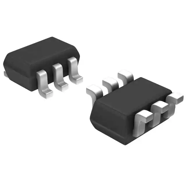
Component Image
26.5 dBm OIP3
Notes:
Output Package marking provides
& Vd
orientation and identification
“53” = Device Code
GND
“X” = Month of Manufacture
“” = Pin 1
GND
53X
GND
GND
Input
WiMAX / WiBRO
CATV & Cable modem
ISM
VCC = 5V
RFin
Pin 3
Applications
Wireless Data / WLAN
Typical Biasing Configuration
Cblock
10 dB IRL and ORL
Cellular / PCS / 3G base station
Top View
Rbias Cbyp
3.2 dB NF
Cbyp
Rbias = (VCC - Vd)/Id
Pin 6
RFout
Vd C
block
Pin 1, 2, 4, 5
(GND)
Attention: Observe precautions for
handling electrostatic sensitive devices.
ESD Machine Model = 160 V
ESD Human Body Model = 2000 V
Refer to Avago Application Note A004R:
Electrostatic Discharge, Damage and Control.
�Absolute Maximum Rating[1] TA=25°C
Thermal Resistance
Symbol
Parameter
Units
Absolute Max.
Id
Device Current
mA
80
PIN,MAX
CW RF Input Power
dBm
18
PDISS
Total Power Dissipation [3]
mW
327
TOPT
Operating Temperature
°C
-40 to 85
TJ,MAX
Junction Temperature
°C
150
TSTG
Storage Temperature
°C
-65 to 150
Thermal Resistance [2] jc = 184°C/W
(Id = 48 mA, Tc = 85°C)
Notes:
1. Operation of this device in excess of any of
these limits may cause permanent damage.
2. Thermal resistance measured using Infrared
measurement technique.
3. Ground lead temperature is 25°C. Derate
5.5mW/°C for Tc >90°C.
Electrical Specifications [1]
TA = 25°C, Zo = 50 , VCC = 5 V, Rbias = 22 , Pin = -15 dBm (unless specified otherwise)
Symbol
Parameter and Test Condition
Id
Device Current
Gp
Power Gain
OIP3 [2]
Output 3rd Intercept Point
Frequency
Units
Min.
Typ.
Max.
mA
44.0
47.6
51.0
18.0
21.8
19.5
21.0
25.0
28.9
26.5
900 MHz
2000 MHz
dB
900 MHz
2000 MHz
dBm
S11
Input Return Loss, 50 source
900 MHz
2000 MHz
dB
-16.5
-12.0
S22
Output Return Loss, 50 load
900MHz
2000 MHz
dB
-17.3
-13.4
S12
Reverse Isolation
900 MHz
2000 MHz
dB
-24.3
-24.7
P1dB
Output Power at 1dB Gain Compression
900 MHz
2000 MHz
dBm
16.0
15.1
NF
Noise Figure
900 MHz
2000 MHz
dB
2.9
3.2
Notes:
1. Measurements obtained on CPWG line with reference plane at the ends of DUT leads (as shown in Figure 1).
2. OIP3 test condition: FRF1 - FRF2 = 10MHz with input power of -23 dBm per tone measured at worse side band.
2
�VCC
Rbias
Bias Tee
RFin
Pin 6
Zo = 50 Ohm
RFout
Zo = 50 Ohm
Pin 3
Pin 1, 2, 4, 5
(GND)
Figure 1. Block diagram of board used for Id, Gain, OIP3, S11, S22, S12, OP1dB and NF measurements.
Circuit losses have been de-embedded from actual measurements.
Product Consistency Distribution Charts at 2 GHz, Vcc = 5 V, Rbias = 22
LSL
43
44
LSL
USL
45
46
47
48
49
50
51
18
Figure 2. Id (mA) distribution. LSL = 44.5, Nominal = 47.6, USL = 50.5
USL
19
20
21
Figure 3. Gain (dB) distribution. LSL = 18, Nominal = 19.5, USL = 21
LSL
Notes:
1. Statistical distribution determined from a sample size of 1500
samples taken from 3 different wafers from 2 wafer lots, measured on
a production test board.
2. Future wafers allocated to this product may have typical values
anywhere between the minimum and maximum specification limits.
25
26
27
Figure 4. OIP3 (dBm) distribution. LSL = 25.5, Nominal = 26.6
3
28
�AVT-53663 Typical Performance Curves
TA = 25°C, Zo = 50 , Pin = -15 dBm (unless specified otherwise)
24
22
P1dB (dBm)
Gain (dB)
20
18
16
14
12
10
0
1
2
3
4
Frequency (GHz)
5
6
Figure 5. Gain vs Frequency at Id = 48mA
17
16
15
14
13
12
11
10
9
8
7
6
5
0
1
2
3
4
Frequency (GHz)
5
6
5
6
Figure 6. P1dB vs Frequency at Id = 48mA
31
6
29
5
25
NF (dB)
OIP3 (dBm)
27
23
21
19
0
1
2
3
4
Frequency (GHz)
5
6
Figure 7. OIP3 vs Frequency at Id = 48mA, Pin = -23dBm
25°C
85°C
-40°C
70
Id (mA)
60
50
40
30
20
10
0
1
2
Figure 9. Id vs Vd and Temperature
4
3
Vd (V)
4
1
0
1
2
3
4
Frequency (GHz)
Figure 8. NF vs Frequency at Id = 48mA
80
0
3
2
17
15
4
5
6
�AVT-53663 Typical Performance Curves
TA = 25°C, Zo = 50 , Pin = -15 dBm (unless specified otherwise), continued
20
22
15
Gain (dB)
P1dB (dBm)
23
21
10
25°C
85°C
-40°C
20
20
30
40
50
Id (mA)
60
70
25°C
85°C
-40°C
5
80
Figure 10. Gain vs Id and Temperature at 900 MHz
20
40
50
Id (mA)
60
70
80
70
80
Figure 11. P1dB vs Id and Temperature at 900 MHz
35
4.0
25°C
85°C
-40°C
3.5
30
NF(dB)
OIP3 (dBm)
30
3.0
25
20
2.5
25°C
85°C
-40°C
20
30
40
50
Id (mA)
60
70
2.0
80
Figure 12. OIP3 vs Id and Temperature at 900 MHz, Pin = -23dBm
20
30
40
50
Id (mA)
60
Figure 13. NF vs Id and Temperature at 900 MHz
20
20
15
Gain (dB)
P1dB (dBm)
21
19
10
25°C
85°C
-40°C
18
20
30
40
50
Id (mA)
Figure 14. Gain vs Id and Temperature at 2 GHz
5
60
70
25°C
85°C
-40°C
80
5
20
30
40
50
Id (mA)
Figure 15. P1dB vs Id and Temperature at 2 GHz
60
70
80
�AVT-53663 Typical Performance Curves
TA = 25°C, Zo = 50 , Pin = -15 dBm (unless specified otherwise), continued
35
4.5
25°C
85°C
-40°C
4.0
30
NF(dB)
OIP3 (dBm)
25°C
85°C
-40°C
25
3.5
3.0
2.5
20
20
30
40
50
Id (mA)
60
70
Figure 16. OIP3 vs Id and Temperature at 2 GHz, Pin = -23dBm
24
16
4.0
14
70
80
0.05
0.9
2.0
2.5
3.0
4.0
10
5.0
6.0
5
20
30
40
50
Id (mA)
60
70
0
80
20
30
40
50
Id (mA)
60
70
80
Figure 19. P1dB vs Id and Frequency (GHz)
40
6.0
0.05
35
0.9
30
2.0
2.5
3.0
4.0
5.0
6.0
25
20
15
6.0
5.5
NF (dB)
OIP3 (dBm)
60
6.0
Figure 18. Gain vs Id and Frequency (GHz)
5.0
5.0
4.5
4.0
4.0
3.0
2.5
2.0
0.9
0.05
3.5
3.0
2.5
20
30
40
50
Id (mA)
60
Figure 20. OIP3 vs Id and Frequency (GHz), Pin = -23dBm
6
50
Id (mA)
5.0
10
10
40
15
12
8
30
20
P1dB (dBm)
18
2.0
2.5
3.0
20
20
Figure 17. NF vs Id and Temperature at 2 GHz
0.05
0.9
22
Gain (dB)
2.0
80
70
80
2.0
20
30
40
50
Id (mA)
Figure 21. NF vs Id and Frequency (GHz)
60
70
80
�AVT-53663 Typical Performance Curves
0
0
-5
-5
-10
-10
S22 (dB)
S11 (dB)
TA = 25°C, Zo = 50 , Pin = -15 dBm (unless specified otherwise), continued
-15
-20
-20
Id=30mA
Id=48mA
Id=60mA
-25
-30
0
2
4
6
Frequency (GHz)
Figure 22. S11 vs Frequency and Id
7
-15
8
Id=30mA
Id=48mA
Id=60mA
-25
10
-30
0
2
4
6
Frequency (GHz)
Figure 23. S22 vs Frequency and Id
8
10
�AVT-53663 Typical Scattering Parameters TA = 25°C, Zo = 50 , Id = 30 mA, (unless specified otherwise)
Frequency
GHz
S11
S21
S12
S22
Mag
Angle
dB
Mag
Angle
Mag
Angle
Mag
Angle
K
0.05
0.14
0.3
21.8
12.35
177.2
0.07
-0.9
0.17
-2.3
1.0
0.1
0.14
0.5
21.8
12.33
174.6
0.07
-1.4
0.17
-5.2
1.0
0.5
0.16
-3.1
21.5
11.95
153.6
0.06
-5.9
0.17
-27.2
1.0
0.9
0.19
-13.0
21.1
11.35
133.4
0.06
-10.1
0.19
-48.1
1.0
1.5
0.25
-32.7
20.2
10.25
104.4
0.06
-15.9
0.23
-79.5
1.1
2.0
0.28
-50.1
19.3
9.26
81.5
0.06
-20.4
0.26
-104.2
1.1
2.5
0.30
-69.3
18.3
8.27
59.8
0.06
-24.3
0.28
-125.7
1.2
3.0
0.31
-89.6
17.3
7.33
39.3
0.06
-27.7
0.30
-144.4
1.2
3.5
0.33
-110.5
16.2
6.47
19.7
0.06
-30.7
0.32
-161.8
1.3
4.0
0.34
-131.5
15.1
5.69
0.7
0.06
-33.4
0.34
-179.0
1.4
4.5
0.35
-152.0
13.9
4.97
-17.5
0.06
-36.0
0.37
164.0
1.4
5.0
0.37
-172.0
12.7
4.30
-35.1
0.06
-38.6
0.39
148.2
1.5
5.5
0.39
168.8
11.4
3.71
-51.9
0.06
-41.3
0.42
133.3
1.6
6.0
0.40
150.6
10.1
3.19
-67.9
0.06
-44.5
0.46
118.8
1.6
6.5
0.42
133.4
8.7
2.73
-83.1
0.06
-48.2
0.49
105.5
1.7
7.0
0.44
117.5
7.4
2.34
-97.4
0.07
-52.3
0.52
93.7
1.7
7.5
0.46
103.1
6.1
2.02
-110.8
0.07
-56.8
0.55
83.4
1.8
8.0
0.49
89.5
4.8
1.74
-123.5
0.07
-61.8
0.56
73.8
1.8
8.5
0.50
76.1
3.6
1.52
-135.9
0.08
-67.6
0.58
64.2
1.9
9.0
0.52
62.3
2.4
1.32
-148.2
0.08
-74.2
0.59
53.7
2.0
9.5
0.54
48.5
1.1
1.14
-160.4
0.08
-81.4
0.60
42.4
2.1
10.0
0.56
35.9
-0.2
0.98
-172.2
0.09
-88.9
0.62
30.7
2.3
10.5
0.58
25.1
-1.6
0.83
176.7
0.09
-96.2
0.64
19.1
2.4
11.0
0.60
16.1
-3.1
0.70
166.6
0.09
-103.0
0.67
8.8
2.6
11.5
0.62
8.1
-4.6
0.59
157.6
0.08
-109.3
0.70
0.0
2.8
12.0
0.64
0.4
-6.1
0.50
149.2
0.08
-115.2
0.73
-7.6
3.0
12.5
0.66
-7.6
-7.4
0.43
141.2
0.08
-121.3
0.74
-14.3
3.2
13.0
0.67
-16.1
-8.7
0.37
133.1
0.08
-127.8
0.75
-20.9
3.5
13.5
0.68
-25.4
-9.8
0.32
124.8
0.08
-135.0
0.75
-28.2
3.9
14.0
0.70
-35.4
-10.9
0.29
115.9
0.09
-143.0
0.74
-37.2
4.4
14.5
0.71
-45.6
-12.0
0.25
106.7
0.09
-151.6
0.74
-47.8
5.0
15.0
0.72
-55.3
-13.3
0.22
97.8
0.08
-160.3
0.74
-59.0
5.5
16.0
0.75
-70.1
-16.1
0.16
83.7
0.08
-174.3
0.78
-76.4
6.6
17.0
0.76
-80.6
-18.9
0.11
76.4
0.07
176.4
0.82
-84.6
7.7
18.0
0.77
-89.5
-21.1
0.09
73.0
0.07
168.7
0.84
-89.0
9.2
19.0
0.78
-99.2
-22.8
0.07
68.3
0.07
158.4
0.82
-98.8
12.0
20.0
0.80
-113.4
-24.7
0.06
59.8
0.07
142.7
0.80
-118.2
16.2
Notes:
1. S-parameters are measured on a CPWG line fabricated on 0.025 inch thick Rogers® RO4350 material. The input reference plane is at the end of the
input lead. The output reference plane is at the end of the output lead.
8
�AVT-53663 Typical Scattering Parameters TA = 25°C, Zo = 50 , Id = 48 mA, (unless specified otherwise)
Frequency
GHz
S11
S21
S12
S22
Mag
Angle
dB
Mag
Angle
Mag
Angle
Mag
Angle
K
0.05
0.08
1.9
22.6
13.46
177.2
0.06
-0.1
0.11
-2.3
1.0
0.1
0.08
4.9
22.6
13.43
174.5
0.06
-1.0
0.11
-5.8
1.0
0.5
0.10
9.3
22.3
12.98
153.1
0.06
-5.3
0.11
-29.6
1.0
0.9
0.15
-0.6
21.8
12.28
132.5
0.06
-9.3
0.14
-51.6
1.0
1.5
0.22
-24.0
20.8
11.00
103.2
0.06
-14.8
0.18
-84.0
1.1
2.0
0.25
-43.0
19.9
9.86
80.3
0.06
-19.0
0.21
-108.9
1.1
2.5
0.27
-63.4
18.8
8.74
58.7
0.06
-22.8
0.24
-130.0
1.2
3.0
0.29
-84.8
17.7
7.71
38.3
0.06
-26.0
0.27
-148.0
1.2
3.5
0.30
-106.7
16.6
6.78
18.9
0.06
-28.8
0.30
-164.9
1.3
4.0
0.32
-128.5
15.5
5.95
0.1
0.06
-31.3
0.32
178.3
1.4
4.5
0.33
-149.6
14.3
5.19
-18.0
0.06
-33.7
0.35
161.5
1.4
5.0
0.35
-170.2
13.1
4.49
-35.5
0.06
-36.1
0.38
146.0
1.5
5.5
0.37
170.1
11.8
3.87
-52.1
0.06
-38.7
0.41
131.4
1.6
6.0
0.39
151.6
10.4
3.33
-68.1
0.06
-41.9
0.45
117.1
1.6
6.5
0.41
134.2
9.1
2.86
-83.2
0.06
-45.7
0.49
104.0
1.6
7.0
0.43
118.1
7.8
2.45
-97.5
0.07
-50.0
0.52
92.4
1.7
7.5
0.45
103.4
6.5
2.11
-110.9
0.07
-54.8
0.54
82.1
1.7
8.0
0.48
89.8
5.2
1.82
-123.6
0.07
-60.0
0.56
72.6
1.7
8.5
0.49
76.3
4.0
1.59
-136.0
0.08
-66.0
0.57
63.0
1.8
9.0
0.51
62.4
2.8
1.38
-148.4
0.08
-72.8
0.58
52.6
1.9
9.5
0.53
48.6
1.5
1.19
-160.6
0.09
-80.3
0.60
41.3
2.0
10.0
0.55
36.0
0.2
1.02
-172.4
0.09
-87.9
0.62
29.6
2.2
10.5
0.58
25.2
-1.2
0.87
176.6
0.09
-95.4
0.64
18.2
2.3
11.0
0.60
16.1
-2.7
0.73
166.5
0.09
-102.3
0.67
8.0
2.5
11.5
0.62
8.1
-4.2
0.62
157.4
0.09
-108.7
0.70
-0.7
2.7
12.0
0.63
0.4
-5.6
0.52
148.9
0.09
-114.7
0.73
-8.2
2.9
12.5
0.65
-7.6
-7.0
0.45
140.9
0.08
-120.9
0.74
-14.9
3.1
13.0
0.67
-16.1
-8.2
0.39
132.8
0.08
-127.5
0.75
-21.5
3.3
13.5
0.68
-25.4
-9.3
0.34
124.3
0.09
-134.7
0.75
-28.8
3.7
14.0
0.69
-35.5
-10.4
0.30
115.3
0.09
-142.8
0.74
-37.7
4.2
14.5
0.71
-45.7
-11.6
0.26
106.0
0.09
-151.5
0.74
-48.4
4.7
15.0
0.72
-55.3
-12.8
0.23
97.0
0.09
-160.2
0.74
-59.5
5.2
16.0
0.75
-70.2
-15.6
0.17
82.7
0.08
-174.3
0.78
-76.8
6.3
17.0
0.76
-80.7
-18.4
0.12
74.9
0.07
176.4
0.82
-84.9
7.4
18.0
0.77
-89.5
-20.6
0.09
71.0
0.07
168.7
0.83
-89.3
8.8
19.0
0.78
-99.3
-22.4
0.08
65.8
0.07
158.4
0.81
-99.1
11.6
20.0
0.80
-113.4
0.0
0.06
56.6
0.07
142.7
0.80
-118.5
15.7
Notes:
1. S-parameters are measured on a CPWG line fabricated on 0.025 inch thick Rogers® RO4350 material. The input reference plane is at the end of the
input lead. The output reference plane is at the end of the output lead.
9
�AVT-53663 Typical Scattering Parameters TA = 25°C, Zo = 50 , Id = 60 mA, (unless specified otherwise)
Frequency
GHz
S11
S21
S12
S22
Mag
Angle
dB
Mag
Angle
Mag
Angle
Mag
Angle
K
0.05
0.06
3.9
22.8
13.81
177.2
0.06
-0.3
0.09
-2.5
1.0
0.1
0.06
8.5
22.8
13.78
174.5
0.06
-1.0
0.09
-5.9
1.0
0.5
0.09
16.0
22.5
13.31
153.0
0.06
-5.1
0.09
-30.4
1.0
0.9
0.13
5.1
22.0
12.58
132.4
0.06
-9.0
0.12
-52.7
1.0
1.5
0.21
-20.7
21.0
11.25
103.1
0.06
-14.4
0.17
-85.2
1.1
2.0
0.24
-40.3
20.1
10.07
80.2
0.06
-18.5
0.20
-110.1
1.1
2.5
0.26
-61.3
19.0
8.92
58.6
0.06
-22.3
0.23
-130.9
1.2
3.0
0.28
-83.1
17.9
7.87
38.3
0.06
-25.5
0.26
-148.7
1.2
3.5
0.29
-105.3
16.8
6.92
19.0
0.05
-28.2
0.29
-165.4
1.3
4.0
0.31
-127.4
15.7
6.07
0.3
0.05
-30.7
0.31
177.9
1.4
4.5
0.32
-148.7
14.5
5.30
-17.8
0.06
-33.0
0.34
161.2
1.4
5.0
0.34
-169.5
13.2
4.59
-35.2
0.06
-35.4
0.38
145.7
1.5
5.5
0.36
170.6
12.0
3.96
-51.9
0.06
-38.0
0.41
131.1
1.6
6.0
0.38
151.9
10.6
3.41
-67.8
0.06
-41.2
0.45
116.9
1.6
6.5
0.40
134.4
9.3
2.92
-83.0
0.06
-45.0
0.48
103.8
1.6
7.0
0.42
118.2
8.0
2.51
-97.3
0.07
-49.3
0.52
92.2
1.6
7.5
0.45
103.5
6.7
2.16
-110.7
0.07
-54.2
0.54
81.9
1.7
8.0
0.47
89.9
5.4
1.87
-123.5
0.08
-59.5
0.56
72.4
1.7
8.5
0.49
76.4
4.2
1.63
-135.9
0.08
-65.6
0.57
62.7
1.8
9.0
0.51
62.5
3.0
1.41
-148.3
0.08
-72.5
0.58
52.3
1.9
9.5
0.53
48.6
1.7
1.22
-160.5
0.09
-80.0
0.60
41.1
2.0
10.0
0.55
35.9
0.4
1.05
-172.3
0.09
-87.7
0.62
29.3
2.1
10.5
0.57
25.1
-1.0
0.89
176.6
0.09
-95.2
0.64
18.0
2.2
11.0
0.60
16.0
-2.5
0.75
166.5
0.09
-102.2
0.67
7.8
2.4
11.5
0.62
8.0
-4.0
0.63
157.3
0.09
-108.6
0.70
-0.9
2.6
12.0
0.63
0.3
-5.4
0.54
148.9
0.09
-114.6
0.72
-8.4
2.8
12.5
0.65
-7.6
-6.8
0.46
140.7
0.09
-120.8
0.74
-15.1
3.0
13.0
0.67
-16.2
-8.0
0.40
132.6
0.09
-127.4
0.75
-21.7
3.2
13.5
0.68
-25.5
-9.1
0.35
124.1
0.09
-134.7
0.75
-29.0
3.6
14.0
0.69
-35.5
-10.2
0.31
115.0
0.09
-142.8
0.74
-37.9
4.1
14.5
0.70
-45.7
-11.3
0.27
105.6
0.09
-151.5
0.73
-48.5
4.6
15.0
0.72
-55.3
-12.6
0.24
96.5
0.09
-160.3
0.74
-59.7
5.1
16.0
0.75
-70.3
-15.4
0.17
82.0
0.08
-174.3
0.78
-77.0
6.1
17.0
0.76
-80.7
-18.1
0.12
74.0
0.07
176.4
0.82
-85.0
7.2
18.0
0.77
-89.5
-20.3
0.10
69.8
0.07
168.6
0.83
-89.4
8.6
19.0
0.78
-99.3
-22.2
0.08
64.3
0.07
158.3
0.81
-99.2
11.3
20.0
0.79
-113.5
-24.1
0.06
54.8
0.07
142.6
0.79
-118.6
15.4
Notes:
1. S-parameters are measured on a CPWG line fabricated on 0.025 inch thick Rogers® RO4350 material. The input reference plane is at the end of the
input lead. The output reference plane is at the end of the output lead.
10
�Part Number Ordering Information
Part Number
No. of Devices
Container
AVT-53663-TR1G
3000
7” Reel
AVT-53663-BLKG
100
Antistatic bag
Package Dimensions
Recommended PCB Pad Layout for
Avago’s SC70 6L/SOT-363 Products
Outline 63 (SOT-363/SC-70)
0.026
HE
E
0.079
0.039
e
D
0.018
Dimensions in inches.
Q1
A2
A
c
A1
L
b
Dimensions (mm)
11
Symbol
Min
Max
E
1.15
1.35
D
1.80
2.25
HE
1.80
2.40
A
0.80
1.10
A2
0.80
1.00
A1
0.00
0.10
Q1
0.10
0.40
e
0.65
b
0.15
0.30
c
0.08
0.25
L
0.10
0.46
Notes:
1. All dimensions are in mm.
2. Dimensions are inclusive of plating.
3. Dimensions are exclusive of mold flash & metal burr.
4. All specifications comply to EIAJSC70.
5. Die is facing up for mold and facing down for trim/form,
ie: reverse trim/form.
6. Package surface to be mirror finish. 0.650BCS.
�Device Orientation
REEL
TOP VIEW
END VIEW
4 mm
8 mm
CARRIER
TAPE
53X
53X
USER
FEED
DIRECTION
COVER TAPE
Tape Dimensions and Product Orientation for Outline 63
P
P2
D
P0
E
F
C
D1
t1 (CARRIER TAPE THICKNESS)
A0
DESCRIPTION
LENGTH
WIDTH
DEPTH
PITCH
BOTTOM HOLE DIAMETER
PERFORATION DIAMETER
PITCH
POSITION
CARRIER TAPE WIDTH
THICKNESS
COVER TAPE WIDTH
TAPE THICKNESS
DISTANCE
CAVITY TO PERFORATION
(WIDTH DIRECTION)
CAVITY TO PERFORATION
(LENGTH DIRECTION)
CAVITY
12
Tt (COVER TAPE THICKNESS)
KO
10° MAX.
10° MAX.
B0
SYMBOL
A0
B0
K0
P
D1
D
P0
E
W
t1
C
Tt
F
P2
W
SIZE (mm)
2.40 ± 0.10
2.40 ± 0.10
1.20 ± 0.10
4.00 ± 0.10
1.00 + 0.25
1.55 ± 0.05
4.00 ± 0.10
1.75 ± 0.10
8.00 ± 0.30
0.254 ± 0.02
5.4 ± 0.10
0.062 ± 0.001
3.50 ± 0.05
SIZE (INCHES)
0.094 ± 0.004
0.094 ± 0.004
0.047 ± 0.004
0.157 ± 0.004
0.039 + 0.010
0.061 ± 0.002
0.157 ± 0.004
0.069 ± 0.004
0.315 ± 0.012
0.0100 ± 0.0008
0.205 ± 0.004
0.0025 ± 0.0004
0.138 ± 0.002
2.00 ± 0.05
0.079 ± 0.002
53X
53X
�Reel Dimension 7 inch
For product information and a complete list of distributors, please go to our web site:
www.avagotech.com
Avago, Avago Technologies, and the A logo are trademarks of Avago Technologies in the United States and other countries.
Data subject to change. Copyright © 2005-2011 Avago Technologies. All rights reserved.
AV02-2359EN - September 29, 2011
�


 工商网监
湘ICP备2023018690号
工商网监
湘ICP备2023018690号
