Data Sheet
HCMS-235x
CMOS Extended Temperature Range
5 × 7 Alphanumeric Display
Description
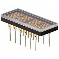
The Broadcom® HCMS-235x sunlight viewable 5 × 7 LED
four-character display is contained in 12-pin dual-inline
packages designed for displaying alphanumeric
information. The display is designed with on-board CMOS
integrated circuits. Two CMOS ICs form an on-board 28-bit
serial-in/parallel-out shift register with constant current
output LED row drivers. Decoded column data is clocked
into the on-board shift register for each refresh cycle. Full
character display is achieved with external column strobing.
Features
On-board low power CMOS IC
Integrated shift register with constant current LED
drivers
Wide operating temperature range
–55°C to +100°C
Compact glass ceramic four-character package
Series X-Y stackable
Sunlight viewable
5 × 7 LED matrix displays full ASCII set
Character height of 5.0 mm (0.20 in.)
Wide viewing angle
X Axis = ±50°
Y Axis = ±65°
Usable in night vision lighting applications
Applications
Broadcom
Avionics
Communication systems
Fire control systems
Radar systems
AV02-0195EN
September 4, 2019
�HCMS-235x Data Sheet
CMOS Extended Temperature Range 5 × 7 Alphanumeric Display
Package Dimensions
20.01
(0.790) MAX.
9
8
7
SEE NOTE 3
4.87
(0.192) REF.
1
2
1
2
4
3
3
PIN 1 MARKED BY DOT
ON BACK OF PACKAGE
4
5
8.43
(0.332)
COO
12 11 10
1.78
(0.070)
1.27
(0.050)
COLOR BIN
DATE CODE
HCMS-23xx XZ
2.79 ± 0.13
(0.110 ± 0.006)
6
5.00 ± 0.13
(0.197 ± 0.005)
CL
3.56
(0.140)
1.27 ± 0.13
(0.050 ± 0.005)
5.08
(0.200)
6.85
(0.270)
2.54
(0.100)
1.27 TYP.
(0.050)
2.54 ± 0.13
(0.100 ± 0.005) TYP.
NON ACCUM.
PART
NUMBER
XXYY
SEE
NOTE 3
2.84
(0.112)REF.
0.54 ± 0.08
(0.020 ± 0.003)
0.25 ± 0.08 TYP.
(0.010 ± 0.003)
6.35 ± 0.25
(0.250 ± 0.010)
LUMINOUS
INTENSITY
CATEGORY
PIN
FUNCTION
1
2
3
4
5
6
COLUMN 1
COLUMN 2
COLUMN 3
COLUMN 4
COLUMN 5
INT. CONNECT*
2.41
(0.095)
PIN 1
PIN FUNCTION
7
8
9
10
11
12
DATA OUT
VB
VDD
CLOCK
GROUND
DATA IN
* DO NOT CONNECT OR USE
NOTES:
1. DIMENSIONS IN MILLIMETERS (INCHES).
2. UNLESS OTHERWISE SPECIFIED, THE
TOLERANCE ON ALL DIMENSIONS IS
± 0.38 mm (± 0.015).
3. CHARACTERS ARE CENTERED WITH RESPECT
TO LEADS WITHIN ± 0.13 mm (± 0.005).
4. LEAD MATERIAL IS COPPER ALLOY,
SOLDER DIPPED.
Absolute Maximum Ratings
Parameter
Value
Supply Voltage VDD to Ground
–0.3V to 7.0V
Data Input, Data Output, VB
–0.3V to VDD
Column Input Voltage, VCOL
–0.3V to VDD
Free Air Operating Temperature Range, TA
–55°C to +100°C
Storage Temperature Range, TS
–55°C to +100°Cb, c
Maximum Allowable Package Power Dissipation, PDb, c at TA = 71°C
1.31W
Through-the-Wave Solder Temperatured
250°C for 3 seconds maximum
Solder Dipping Temperatured
260°C for 5 seconds maximum
ESD Protection at1.5 kΩ, 100 pF
VZ= 4 kV
a
a. Maximum duration 2 seconds.
b. Maximum allowable power dissipation is derived from VDD = 5.25V, VB = 2.4V, VCOL = 3.5V, 20 LEDs ON per
character, 20% DF.
c. HCMS-2353 derate above 71°C at 23 mW/°C, RJ-A = 45°C/W.
Derating based on RJ-A = 35°C/W per display for printed circuit board assembly.
d. 1.59 mm (0.063 in.) below body.
Broadcom
AV02-0195EN
2
�HCMS-235x Data Sheet
CMOS Extended Temperature Range 5 × 7 Alphanumeric Display
Recommended Operating Conditions
Over Operating Range (–55°C to +100°C)
Parameter
Symbol
Min.
Typ.
Max.
Units
Supply Voltage
VDD
4.75
5.00
5.25
V
Data Out Current, Low State
IOL
—
—
1.6
mA
Data Out Current, High State
IOH
—
—
–0.5
mA
Column Input Voltage
VCOL
2.75
3.0
3.5
V
Setup Time
tSETUP
10
—
—
ns
Hold Time
tHOLD
25
—
—
ns
Clock Pulse Width High
tWH(CLOCK)
50
—
—
ns
Clock Pulse Width Low
tWL(CLOCK)
50
—
—
ns
Clock High to Low Transition
tTHL
—
—
200
ns
Clock Frequency
fCLOCK
—
5
MHz
Broadcom
AV02-0195EN
3
�HCMS-235x Data Sheet
CMOS Extended Temperature Range 5 × 7 Alphanumeric Display
Electrical Characteristics Over Operating Range (–55°C to + 100°C)
Parameter
Min.
Typ.a
Max.
Units
fCLOCK = 5 MHz
—
6.2
7.8
mA
IDDDSoff
VB = 0.4V, Data and Clock = 0.4V
—
1.8
26
mA
IDDDSon
VB = 2.4V, Data and Clock = 0.4V
—
2.2
6.0
Symbol
IDDD
b
Supply Current, Dynamic
c
Supply Current, Static
Column Input Current
ICOL
Test Conditions
VB = 0.4V
—
—
10
µA
VB = 2.4V
—
500
650
mA
—
V
0.8
V
Input Logic High Data, VB, Clock
VIH
VDD = 4.75V
2.0
Input Logic Low Data, VB, Clock
VIL
VDD = 5.25V
—
II
VDD = 5.25V
Input Current
—
—
µA
Data
Vd = 2.4V (Logic High) or
–46
–60
–103
Clock, VB
Vd = 0.4V (Logic Low)
–92
–120
–206
VDD = 4.75V
2.4
4.2
—
V
—
0.2
0.4
V
—
668
—
mW
—
10
—
°C/W
—
—
5 ×10⁻⁸
cc/second
Data Out Voltage
VOH
IOH = –0.5 mA
ICOL = 0 mA
VOL
VDD = 5.25V
IOL = 1.6 mA
ICOL = 0 mA
e
Power Dissipation Per Package
PD
VDD = 5.0V
VCOL = 3.5V
17.5% DF
VB = 2.4V
15 LEDs ON per Character
Thermal Resistance
RθJ-PIN
IC Junction-to-Pinf
Leak Rate
a. All typical values specified at VDD = 5.0V and TA = 25°C.
b. IDD Dynamic is the IC current while clocking column data through the on-board shift register at a clock frequency of 5 MHz, the display is not
illuminated.
c. IDD Static is the IC current after column data is loaded and not being clocked through the on-board shift register.
d. VI represents the input voltage to an input pin.
e. Four characters are illuminated with a typical ASCII character composed of 15 dots per character.
f. IC junction temperature TJ (IC) = (PD)(RθJ-PIN + RθPC-A) + TA.
Broadcom
AV02-0195EN
4
�HCMS-235x Data Sheet
CMOS Extended Temperature Range 5 × 7 Alphanumeric Display
Optical Characteristics at TA = 25°C
High Performance Green, HCMS-2353
Description
Peak Luminous Intensity per LEDb
(Character Average)
Symbol
IvPEAK
Test Conditions
VDD = 5.0V
Min.
Typ.a
Max.
Units
2400
3000
—
µcd
VCOL = 3.5V
VB = 2.4V
Ti = 25°Cc
Dominant Wavelengthd, e
d
—
574
—
nm
Peak Wavelength
PEAK
—
568
—
nm
a. All typical values specified at VDD = 5.0V and TA = 25°C unless otherwise noted.
b. These LED displays are categorized for luminous intensity, with the intensity category designated by a letter code on the back of the package.
c. Ti refers to the initial case temperature of the display immediately prior to the light measurement.
d. Dominant wavelength, d, is derived from the CIE Chromaticity Diagram, and represents the single wavelength that defines the color of the
device.
e. Categorized for color with the color category designated by a number on the back of the package.
Yellow, HCMS-2351
Description
Peak Luminous Intensity per LEDb
(Character Average)
Symbol
IvPEAK
Test Condition
VDD = 5.0V
Min
Typ.a
Max.
Units
1600
2400
—
mcd
VCOL = 3.5V
VB = 2.4V
Ti = 25°Cc
Dominant Wavelengthd, e
d
—
—
585
—
nm
Peak Wavelength
PEAK
—
—
583
—
nm
a. All typical values specified at VDD = 5.0V and TA = 25°C unless otherwise noted.
b. These LED displays are categorized for luminous intensity, with the intensity category designated by a letter code on the back of the package.
c. Ti refers to the initial case temperature of the display immediately prior to the light measurement.
d. Dominant wavelength, d, is derived from the CIE Chromaticity Diagram, and represents the single wavelength that defines the color of the
device.
e. Categorized for color with the color category designated by a number on the back of the package.
Broadcom
AV02-0195EN
5
�HCMS-235x Data Sheet
CMOS Extended Temperature Range 5 × 7 Alphanumeric Display
Switching Characteristics
1/fCLOCK
Parameter
tTHL
tWH
VIH
CLOCK
VIL
DATA IN
VIH
VIL
fclock CLOCK Rate
tWL
2.0 V
0.8 V
tHOLD
tSETUP
CL = 15 pf
Propgation Delay
CLOCK to DATA OUT
RL = 2.4 kΩ
2.4 V
0.4 V
VIH
VB
VIL
ON (ILLUMINATED)
DISPLAY
OFF (NOT ILLUMINATED)
Typ.
Max.
Units
—
5
MHz
—
105
ns
4
5
µs
1
2
VB (0.4V) to
Display OFF
0.8 V
tPLH, tPHL
Broadcom
tPLH, tPHL
tOFF
2.0 V
DATA OUT
Condition
VOH
VOL
tON
VB (2.4V) to
Display ON
2.0 V
0.8 V
tOFF
tON
90%
10%
AV02-0195EN
6
�HCMS-235x Data Sheet
CMOS Extended Temperature Range 5 × 7 Alphanumeric Display
Electrical Description
To load decoded character information into the display,
column data for character 4 is loaded first, and the column
data for character 1 is loaded last in the following manner.
The 7 data bits for column 1, character 4, are loaded into the
on-board shift register. Next, the 7 data bits for column 1,
character 3, are loaded into the shift register, shifting the
character 4 data over one character position.
The display contains four 5 x 7 LED dot matrix characters
and two CMOS integrated circuits, as shown in Figure 1.
The two CMOS integrated circuits form an on-board 28-bit
serial-in/parallel-out shift register that accepts standard TTL
logic levels. The Data Input, pin 12, is connected to bit
position 1 and the Data Output, pin 7, is connected to bit
position 28. The shift register puts out control constant
current sinking LED row drivers. A logic 1 stored in the shift
register enables the corresponding LED row driver and a
logic 0 stored in the shift register disables the corresponding
LED row driver.
This process is repeated for the other two characters until all
28 bits of column data (four 7-bit bytes of character column
data) are loaded into the on-board shift register. Then the
column 1 input, VCOL pin 1, is energized to illuminate
column 1 in all four characters. This process is repeated for
columns 2, 3, 4, and 5. All VCOL inputs should be at logic low
to ensure that the display is off when loading data. The
display is blank when the blanking input VB, pin 8, is at logic
low regardless of the outputs of the shift register or whether
one of the VCOL inputs is energized. Refer to Application
Note 1016 for drive circuit information.
The electrical configuration of these CMOS IC
alphanumeric displays allows for an effective interface to a
display controller circuit, which supplies decoded character
information. The row data for a given column (one 7-bit byte
per character) is loaded (bit serial) into the on-board 28-bit
shift register with high-to-low transitions of the clock input.
Figure 1: Display Block Diagram
COLUMN DRIVE INPUTS
COLUMN
1 2 3 4 5
LED
MATRIX
2
BLANKING
CONTROL, VB
SERIAL
DATA
INPUT
1 2 3 4 5 6 7
ROWS
1 2 3 4 5 6 7
LED
MATRIX
3
ROWS 1-7
ROWS 1-7
LED
MATRIX
4
ROWS 1-7
CONSTANT CURRENT SINKING LED DRIVERS
ROWS 8-14
ROWS 15-21
28-BIT SIPO SHIFT REGISTER
ROWS 22-28
SERIAL
DATA
OUTPUT
CLOCK
Broadcom
AV02-0195EN
7
�HCMS-235x Data Sheet
CMOS Extended Temperature Range 5 × 7 Alphanumeric Display
ESD Susceptibility
Night Vision Lighting
The display has an ESD susceptibility rating of Class 3 of
MIL-STD-883E, HBM. Take normal CMOS handling
precautions when handling these devices.
When used with the proper NVG/DV filters, the HCMS-235x
display may be used in night vision lighting applications. For
a list of NVG/DV filters and a description on night vision
lighting technology, refer to Application Note 1030, LED
Displays and Indicators and Night Vision Imaging System
Lighting.
Soldering and Post Solder
Cleaning
These displays may be soldered with a standard wave
solder process using either an RMA flux and solvent
cleaning or an OA flux and aqueous cleaning. For optimum
soldering, the solder wave temperature should be 245°C,
and the dwell time for any display lead passing through the
wave should be 1.5 to 2 seconds. For more detailed
information, refer to Application Note 1027, Soldering LED
Components.
Contrast Enhancement
Controller Circuits, Power
Calculations, and Display
Dimming
Refer to Application Note 1016, Using the HDSP-2000
Alphanumeric Display Family, for information on controller
circuits to drive these displays, how to do power
calculations, and a technique for display dimming.
Figure 2: Peak Column Current vs. Column Voltage at
TA = 25°C
When used with the proper contrast enhancement filters,
the display is readable in sunlight.
ICOL - PEAK COLUMN CURRENT - mA
Refer to Application Note 1029, Luminous Contrast and
Sunlight Readability of the HDSP-235X Series
Alphanumeric Displays for Sunlight Viewable Applications,
for information on contrast enhancement for sunlight and
daylight ambient. Refer to Application Note 1015, Contrast
Enhancement Techniques for LED Displays, for information
on contrast enhancement in moderate ambients.
600
500
400
300
200
100
0
Broadcom
0
1
2
3
4
VCOL - COLUMN VOLTAGE - V
5
6
AV02-0195EN
8
�HCMS-235x Data Sheet
CMOS Extended Temperature Range 5 × 7 Alphanumeric Display
Intensity Bin Limits
Intensity Bin Limits for HCMS-2351
Color Bin Limits
Intensity Range (mcd)
Bin
Min.
QA
Max.
Color
Color Bin
Min.
Max.
Yellow
Q
11.197
15.774
3
581.5
585.0
R
13.437
19.718
4
584.0
587.5
S
16.797
23.662
5
586.5
590.0
T
20.156
29.577
6
589.0
592.5
U
25.195
35.492
Green
Intensity Bin Limits for HCMS-2353
Intensity Range (mcd)
Bin
Min.
Max.
S
16.797
23.662
T
20.156
29.577
U
25.195
35.492
V
30.234
44.366
W
37.739
52.239
NOTE:
7
591.5
595.0
1
576.0
580.0
2
573.0
577.0
3
570.0
574.0
4
567.0
571.0
Test conditions as specified in Optical
Characteristics at TA = 25°C.
Option Code Definition
H
C
M
S
-
2
3
5
x
-
x1
x2
x3
x
x
lv Bin Range Identifier
x1 x2
x1
Minimum Iv bin
x2
Maximum Iv bin
Color Bin Range Identifier
x3
Broadcom
A
Color bin 2 or 3
B
Color bin 4 or 5
C
Color bin 5 or 6
D
Color bin 3 or 4
AV02-0195EN
9
�Broadcom, the pulse logo, Connecting everything, Avago Technologies, Avago, and the A logo are among the trademarks
of Broadcom and/or its affiliates in the United States, certain other countries, and/or the EU.
Copyright © 2008–2019 Broadcom. All Rights Reserved.
The term “Broadcom” refers to Broadcom Inc. and/or its subsidiaries. For more information, please visit www.broadcom.com.
Broadcom reserves the right to make changes without further notice to any products or data herein to improve reliability,
function, or design. Information furnished by Broadcom is believed to be accurate and reliable. However, Broadcom does
not assume any liability arising out of the application or use of this information, nor the application or use of any product or
circuit described herein, neither does it convey any license under its patent rights nor the rights of others.
�