HCMS-29xx Series
High Performance CMOS 5 x 7 Alphanumeric Displays
Data Sheet
Description
Features
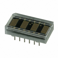
The HCMS-29xx series are high performance, easy
to use dot matrix displays driven by on-board CMOS ICs.
Each display can be directly interfaced with a microproces
sor, thus eliminating the need for cumbersome interface
components. The serial IC interface allows higher charac
ter count information displays with a minimum of data
lines. A variety of colors, font heights, and character
counts gives designers a wide range of product choices
for their specific applications and the easy to read 5 x 7
pixel format allows the display of uppercase, lower case,
Katakana, and custom user-defined characters. These dis
plays are stackable in the x- and y- directions, making
them ideal for high character count displays.
• Easy to use
• Interfaces directly with microprocessors
• 0.15” character height in 4, 8, and 16 (2x8) character
packages
• 0.20” character height in 4 and 8 character packages
• Rugged X- and Y-stackable package
• Serial input
• Convenient brightness controls
• Wave solderable
• Offered in five colors
• Low power CMOS technology
• TTL compatible
Applications
• Telecommunications equipment
• Portable data entry devices
• Computer peripherals
• Medical equipment
• Test equipment
• Business machines
• Avionics
• Industrial controls
Device Selection Guide
Description
1 x 4 0.15” Character
1 x 8 0.15” Character
2 x 8 0.15” Character
1 x 4 0.20” Character
1 x 8 0.20” Character
AlGaAs
HCMS-
2905
2915
2925
2965
2975
HER
HCMS-
2902
2912
2922
2962
2972
Orange
HCMS-
2904
2914
2924
2964
2974
Yellow
HCMS-
2901
2911
2921
2961
2971
Green
HCMS-
2903
2913
2923
2963
2973
Package
Drawing
A
B
C
D
E
ESD WARNING: STANDARD CMOS HANDLING PRECAUTIONS SHOULD BE OBSERVED TO AVOID STATIC DISCHARGE.
�HCMS-290x
17.78 (0.700) MAX.
PIN FUNCTION
ASSIGNMENT TABLE
PIN # FUNCTION
4.45 (0.175) TYP.
1
2
3
4
5
6
7
8
9
10
11
12
2.22 (0.087) SYM.
12
3.71 (0.146) TYP.
1
2
3
4
10.16 (0.400) MAX.
1
DATA OUT
OSC
V LED
DATA IN
RS
CLK
CE
BLANK
GND
SEL
V LOGIC
RESET
2.11 (0.083) TYP.
DATE CODE
LIGHT INTENSITY CATEGORY
COLOR BIN
COUNTRY OF ORIGIN
PIN # 1 IDENTIFIER
PART NUMBER
5.08
(0.200)
0.25
(0.010)
HCMS-290X X Z
YYWW COO
4.32
TYP.
(0.170)
0.51 (0.020)
PIN # 1
2.54
SYM.
(0.100)
1.27
(0.050) SYM.
2.54 ± 0.13 TYP.
(0.100 ± 0.005)
(NON ACCUM.)
0.51 ± 0.13 TYP.
(0.020 ± 0.005)
7.62
(0.300)
NOTES:
1. DIMENSIONS ARE IN mm (INCHES).
2. UNLESS OTHERWISE SPECIFIED, TOLERANCE ON DIMENSIONS IS ± 0.38 mm (0.015 INCH).
3. LEAD MATERIAL: SOLDER PLATED COPPER ALLOY.
HCMS-291x
35.56 (1.400) MAX.
2.22 (0.087) SYM.
4.45
(0.175) TYP.
3.71
TYP.
(0.146)
PIN FUNCTION
ASSIGNMENT TABLE
26
0
1
2
3
4
5
6
7
PIN # FUNCTION
10.16 (0.400) MAX.
3
2.11 (0.083) TYP.
DATE CODE (YEAR, WEEK)
PIN # 1 IDENTIFIER
INTENSITY CATEGORY
COLOR BIN
PART NUMBER
COUNTRY OF ORIGIN
0.51
(0.020)
HCMS-291X
YYWW
X
Z
COO
0.25
(0.010)
5.08 (0.200)
4.32
(0.170)TYP.
2.54
SYM.
(0.100)
0.51 ± 0.13
TYP.
(0.020 ± 0.005)
2.54 ± 0.13
TYP.
(0.100 ± 0.005)
(NON ACCUM.)
1.27
SYM.
(0.050)
NOTES:
1. DIMENSIONS ARE IN mm (INCHES).
2. UNLESS OTHERWISE SPECIFIED, TOLERANCE ON DIMENSIONS IS ± 0.38 mm (0.015 INCH).
3. LEAD MATERIAL: SOLDER PLATED COPPER ALLOY.
�
7.62
(0.300)
1
2
3
4
5
6
7
8
9
10
11
12
13
14
15
16
17
18
19
20
21
22
23
24
25
26
NO PIN
NO PIN
V LED
NO PIN
NO PIN
NO PIN
GND LED
NO PIN
NO PIN
V LED
NO PIN
NO PIN
NO PIN
DATA IN
RS
NO PIN
CLOCK
CE
BLANK
GND LOGIC
SEL
V LOGIC
NO PIN
RESET
OSC
DATA OUT
�HCMS-292x
PIN FUNCTION ASSIGNMENT TABLE
35.56 (1.400) MAX.
2.22 (0.088) SYM.
4.45 (0.175) MAX.
26B
ROW B
0
1
2
3
4
5
6
7
3B
9.65 (0.380)
4.83
(0.190)
19.81 (0.780) MAX.
26A
8
ROW A
9
10
11
12
13
14
15
3.71 (0.146) TYP.
3A
2.11 (0.083) TYP.
DATE CODE (YEAR, WEEK)
PIN # 1 IDENTIFIER
INTENSITY CATEGORY
COLOR BIN
PART NUMBER
PIN # FUNCTION
PIN # FUNCTION
1A
2A
3A
4A
5A
6A
7A
8A
9A
10A
11A
12A
13A
14A
15A
16A
17A
18A
19A
20A
21A
22A
23A
24A
25A
26A
1B
2B
3B
4B
5B
6B
7B
8B
9B
10B
11B
12B
13B
14B
15B
16B
17B
18B
19B
20B
21B
22B
23B
24B
25B
26B
NO PIN
NO PIN
V LED
NO PIN
NO PIN
NO PIN
GND LED
NO PIN
NO PIN
V LED
NO PIN
NO PIN
NO PIN
DATA IN
RS
NO PIN
CLOCK
CE
BLANK
GND LOGIC
SEL
V LOGIC
NO PIN
RESET
OSC
DATA OUT
COUNTRY OF ORIGIN
HCMS-292X
YYWW
0.51
(0.020)
X
Z
COO
0.25
(0.010)
5.08 (0.200)
2.54
(0.100) SYM.
0.51 ± 0.13
TYP.
(0.020 ± 0.005)
1.27
(0.050)
2.03
(0.080)
2.54 ± 0.13
TYP.
(0.100 ± 0.005)
(NON ACCUM.)
7.62
(0.300)
NOTES:
1. DIMENSIONS ARE IN mm (INCHES).
2. UNLESS OTHERWISE SPECIFIED, TOLERANCE ON DIMENSIONS IS ± 0.38 mm (0.015 INCH).
3. LEAD MATERIAL: SOLDER PLATED COPPER ALLOY.
HCMS-296x
PIN FUNCTION
ASSIGNMENT TABLE
PIN # FUNCTION
21.46 (0.845) MAX.
1
2
3
4
5
6
7
8
9
10
11
12
2.67 (0.105) SYM.
2.54 (0.100) TYP.
4.57
(0.180)TYP.
0
1
2
3
11.43 (0.450) MAX.
DATA OUT
OSC
V LED
DATA IN
RS
CLK
CE
BLANK
GND
SEL
V LOGIC
RESET
5.36 (0.211) TYP.
PIN # 1 IDENTIFIER
DATE CODE (YEAR, WEEK)
INTENSITY CATEGORY
COLOR BIN
COUNTRY OF ORIGIN
PART NUMBER
HCMS-296X
YYWW
X Z
0.25
(0.010)
5.31
(0.209)
COO
0.51 ± 0.13
TYP.
(0.020 ± 0.005)
2.54 ± 0.13 TYP.
(0.100 ± 0.005)
1.83
(0.072) SYM.
NOTES:
1. DIMENSIONS ARE IN mm (INCHES).
2. UNLESS OTHERWISE SPECIFIED, THE TOLERANCE ON DIMENSIONS IS ± 0.38 mm (0.015 INCH).
3. LEAD MATERIAL: SOLDER PLATED COPPER ALLOY.
�
3.71
TYP.
(0.146)
0.50
(0.020)
4.28
(0.169) SYM.
7.62
(0.300)
NO PIN
NO PIN
V LED
NO PIN
NO PIN
NO PIN
GND LED
NO PIN
NO PIN
V LED
NO PIN
NO PIN
NO PIN
DATA IN
RS
NO PIN
CLOCK
CE
BLANK
GND LOGIC
SEL
V LOGIC
NO PIN
RESET
OSC
DATA OUT
�HCMS-297x
42.93 (1.690) MAX.
2.67 (0.105) SYM.
5.36 (0.211) TYP.
PIN FUNCTION
ASSIGNMENT TABLE
26
4.57
(0.180) TYP.
1
2
3
4
5
6
7
8
PIN # FUNCTION
11.43 (0.450) MAX.
3
2.54 (0.100) TYP.
PIN # 1 IDENTIFIER
DATE CODE (YEAR, WEEK)
INTENSITY CATEGORY
COLOR BIN
COUNTRY OF ORIGIN
PART NUMBER
0.51
(0.020)
HCMS-297X
YYWW
0.25
(0.010)
5.31
(0.209)
X Z
COO
3.71
TYP.
(0.146)
6.22
SYM.
(0.245)
0.51 ± 0.13
(0.020 ± 0.005) TYP.
1.90
(0.075) SYM.
2.54 ± 0.13 TYP.
(0.100 ± 0.005)
(NON ACCUM.)
7.62
(0.300)
NOTES:
1. DIMENSIONS ARE IN mm (INCHES).
2. UNLESS OTHERWISE SPECIFIED, TOLERANCE ON DIMENSIONS IS ± 0.38 mm (0.015 INCH).
3. LEAD MATERIAL: SOLDER PLATED COPPER ALLOY.
Absolute Maximum Ratings
Logic Supply Voltage, VLOGIC to GNDLOGIC ‑0.3 V to 7.0 V
LED Supply Voltage, VLED to GNDLED ‑0.3 V to 5.5 V
Input Voltage, Any Pin to GND ‑0.3 V to VLOGIC +0.3 V
Free Air Operating Temperature Range TA[1] ‑40°C to +85°C
Relative Humidity (noncondensing)
85%
Storage Temperature, TS ‑55°C to 100°C
Soldering Temperature [1.59 mm (0.063 in.) Below Body]
Solder Dipping
260°C for 5 secs
Wave Soldering
250°C for 3 secs
ESD Protection @ 1.5 kΩ, 100 pF (each pin)
Class 1, 0-1999 V
[2]
TOTAL Package Power Dissipation at TA = 25°C
4 Character
1.2 W
8 Character
2.4 W
16 Character
4.8 W
Note:
1. For operation in high ambient temperatures, see Appendix A, Thermal Considerations.
Recommended Operating Conditions Over Temperature Range (-40°C to +85°C)
Parameter
Symbol
Min.
Typ.
Max.
Units
Logic Supply Voltage
VLOGIC
3.0
5.0
5.5
V
LED Supply Voltage
VLED
4.0
5.0
5.5
V
GNDLED to GNDLOGIC
–
-0.3
0
+0.3
V
�
1
2
3
4
5
6
7
8
9
10
11
12
13
14
15
16
17
18
19
20
21
22
23
24
25
26
NO PIN
NO PIN
V LED
NO PIN
NO PIN
NO PIN
GND LED
NO PIN
NO PIN
V LED
NO PIN
NO PIN
NO PIN
DATA IN
RS
NO PIN
CLOCK
CE
BLANK
GND LOGIC
SEL
V LOGIC
NO PIN
RESET
OSC
DATA OUT
�Electrical Characteristics Over Operating Temperature Range (-40°C to +85°C)
TA = 25°C
-40°C < TA < 85°C
VLOGIC = 5.0 V
3.0 V < VLOGIC < 5.5 V
Parameter
Symbol
Typ.
Max.
Min.
Max.
Units
Input Leakage Current
II
µA
HCMS-290X/296X (4 char)
+7.5
-2.5
+50
HCMS-291X/297X (8 char)
+15
-5.0
+100
HCMS-292X (16 char)
+15
-5.0
+100
ILOGIC OPERATING
ILOGIC(OPT)
mA
HCMS-290X/296X (4 char)
0.4
2.5
5
HCMS-291X/297X (8 char)
0.8
5
10
HCMS-292X (16 char)
0.8
5
10
ILOGIC SLEEP[1]
ILOGIC(SLP)
µA
HCMS-290X/296X (4 char)
5
15
25
HCMS-291X/297X (8 char)
10
30
50
HCMS-292X (16 char)
10
30
50
ILED BLANK
ILED(BL)
mA
HMCS-290X/296X (4 char)
2.0
4
4.0
HCMS-291X/297X (8 char)
4.0
8
8
HCMS-292X (16 char)
4.0
8
8
[1]
ILED SLEEP
ILED(SLP)
µA
HCMS-290X/296X (4 char)
1
3
50
HCMS 291X/297X (8 char)
2
6
100
HCMS-292X (16 char)
2
6
100
Peak Pixel Current[2]
IPIXEL
HCMS-29X5 (AlGaAs)
15.4 17.1
18.7
mA
HCMS-29XX (Other Colors)
14.0 15.9
17.1
mA
pixel
HIGH Level Input Voltage
Vih
2.0
V
0.8 VLOGIC
V
LOW Level Input Voltage
Vil
0.8
V
0.2 VLOGIC V
HIGH Level Output Voltage Voh
2.0
V
0.8 VLOGIC
V
LOW Level Output Voltage Vol
0.4
V
0.2 VLOGIC V
Thermal Resistance
RqJ-P
70
°C/W
Test Conditions
VIN = 0 V to VLOGIC
VIN = VLOGIC
VIN = VLOGIC
BL = 0 V
VLED = 5.5 V
All pixels ON,
Average value per
4.5 V < VLOGIC < 5.5 V
3.0 V < VLOGIC < 4.5 V
4.5 V < VLOGIC < 5.5 V
3.0 V < VLOGIC < 4.5 V
VLOGIC = 4.5 V,
Ioh = -40 µA
3.0 V < VLOGIC < 4.5 V
VLOGIC = 5.5 V,
Iol = 1.6 mA[3]
3.0 V < VLOGIC < 4.5 V
IC junction to pin
Notes:
1. In SLEEP mode, the internal oscillator and reference current for LED drivers are off.
2. Average peak pixel current is measured at the maximum drive current set by Control Register 0. Individual pixels may exceed this value.
3. For the Oscillator Output, Iol = 40 µA.
�
�Optical Characteristics at 25°C[1]
VLED = 5.0 V, 50% Peak Current, 100% Pulse Width
Luminous Intensity per LED[2]
Character Average (µcd)
Display Color
Part Number
Min.
Typ.
AlGaAs Red
HCMS-29X5
95
230
High Efficiency Red
HCMS-29X2
29
64
Orange
HCMS-29X4
29
64
Yellow
HCMS-29X1
29
64
Green
HCMS-29X3
57
114
Peak
Wavelength
lPeak (nm)
Typ.
645
635
600
583
568
Dominant
Wavelength
ld[3] (nm)
Typ.
637
626
602
585
574
Notes:
1. Refers to the initial case temperature of the device immediately prior to measurement.
2. Measured with all LEDs illuminated.
3. Dominant wavelength, ld, is derived from the CIE chromaticity diagram and represents the single wavelength which defines the perceived
LED color.
Electrical Description
Pin Function
RESET (RST)
Description
Sets Control Register bits to logic low. The Dot Register contents are unaffected by
the Reset pin. (logic low = reset; logic high = normal operation).
DATA IN (DIN)
Serial Data input for Dot or Control Register data. Data is entered on the rising edge
of the Clock input.
DATA OUT (DOUT )
Serial Data output for Dot or Control Register data. This pin is used for cascading
multiple displays.
CLOCK (CLK)
Clock input for writing Dot or Control Register data. When Chip Enable is logic low,
data is entered on the rising Clock edge.
REGISTER SELECT (RS)
Selects Dot Register (RS = logic low) or Control Register (RS = logic high) as the destination for serial data entry. The logic level of RS is latched on the falling edge of the
Chip Enable input.
CHIP ENABLE (CE)
This input must be a logic low to write data to the display. When CE returns to logic
high and CLK is logic low, data is latched to either the LED output drivers or a Control
Register.
OSCILLATOR SELECT (SEL)
Selects either an internal or external display oscillator source. (logic low = External
Display Oscillator; logic high = Internal Display Oscillator).
OSCILLATOR (OSC)
Output for the Internal Display Oscillator (SEL = logic high) or input for an External
Display Oscillator (SEL = logic low).
BLANK (BL)
Blanks the display when logic high. May be modulated for brightness control.
GNDLED
Ground for LED drivers.
GNDLOGIC
Ground for logic.
VLED
Positive supply for LED drivers.
VLOGIC
Positive supply for logic.
�
�AC Timing Characteristics Over Temperature Range (-40°C to +85°C)
Timing
Diagram Ref.
Number
Description Symbol
4.5 V < VLOGIC VLOGIC)
and when a high current is forced into the input. To
prevent input current latchup and ESD damage, unused
inputs should be connected to either ground or VLOGIC.
Voltages should not be applied to the inputs until VLOGIC
has been applied to the display.
The average current required by the display can be
calculated with Equation 4.
The power supply has to be able to supply IPEAK transients and supply ILED(AVG) continuously. The range on
VLED allows noise on this supply without significantly
changing the display brightness.
VLOGIC and VLED Considerations
The display uses two independent electrical systems.
One system is used to power the display’s logic and the
other to power the display’s LEDs. These two systems
keep the logic supply clean.
Separate electrical systems allow the voltage applied
to VLED and VLOGIC to be varied independently. Thus,
VLED can vary from 0 to 5.5 V without affecting either
the Dot or the Control Registers. VLED can be varied
between 4.0 to 5.5 V without any noticeable variation in
light output. However, operating VLED below 4.0 V may
cause objectionable mismatch between the pixels and is
not recommended. Dimming the display by pulse width
modulating VLED is also not recommended.
VLOGIC can vary from 3.0 to 5.5 V without affecting either
the displayed message or the display intensity. However,
operation below 4.5 V will change the timing and logic
levels and operation below 3 V may cause the Dot and
Control Registers to be altered.
The logic ground is internally connected to the LED
ground by a substrate diode. This diode becomes forward biased and conducts when the logic ground is 0.4
V greater than the LED ground. The LED ground and
the logic ground should be connected to a common
ground which can withstand the current introduced by
the switching LED drivers. When separate ground connections are used, the LED ground can vary from ‑0.3
V to +0.3 V with respect to the logic ground. Voltages
below ‑0.3 V can cause all the dots to be ON. Voltage
above +0.3 V can cause dimming and dot mismatch. The
LED ground for the LED drivers can be routed separately
from the logic ground until an appropriate ground
plane is available. On long interconnections between
the display and the host system, voltage drops on the
analog ground can be kept from affecting the display
logic levels by isolating the two grounds.
15
Appendix C. Oscillator
The oscillator provides the internal refresh circuitry with
a signal that is used to synchronize the columns and
rows. This ensures that the right data is in the dot drivers for that row. This signal can be supplied from either
an external source or the internal source.
A display refresh rate of 100 Hz or faster ensures
flicker‑free operation. Thus for an external oscillator
the frequency should be greater than or equal to 512
x 100 Hz = 51.2 kHz. Operation above 1 MHz without
the prescaler or 8 MHz with the prescaler may cause
noticeable pixel to pixel mismatch.
Appendix D. Refresh Circuitry
This display driver consists of 20 one‑of‑eight column
decoders and 20 constant current sources, 1 one‑of‑eight
row decoder and eight row sinks, a pulse width modulation control block, a peak current control block, and the
circuit to refresh the LEDs. The refresh counters and oscillator are used to synchronize the columns and rows.
The 160 bits are organized as 20 columns by 8 rows. The
IC illuminates the display by sequentially turning ON each
of the 8 row‑drivers. To refresh the display once takes
512 oscillator cycles. Because there are eight row drivers, each row driver is selected for 64 (512/8) oscillator
cycles. Four cycles are used to briefly blank the display
before the following row is switched on. Thus, each row
is ON for 60 oscillator cycles out of a possible 64. This
corresponds to the maximum LED on time.
�Appendix E. Display Brightness
Two ways have been shown to control the brightness
of this LED display: setting the peak current and setting
the duty factor. Both values are set in Control Word 0.
To compute the resulting display brightness when both
PWM and peak current control are used, simply multiply the two relative brightness factors. For example, if
Control Register 0 holds the word 1001101, the peak
current is 73% of full scale (BIT D5 = L, BIT D4 = L) and
the PWM is set to 60% duty factor (BIT D3 = H, BIT D2
= H, BIT D1 = L, BIT D0 = H). The resulting brightness is
44% (.73 x .60 = .44) of full scale.
The temperature of the display will also affect the LED
brightness as shown in Figure 5.
RELATIVE LUMINOUS INTENSITY
(NORMALIZED TO 1 AT 25°C)
3.0
2.6
HER/ORANGE
2.2
YELLOW
1.8
GREEN
1.4
AlGaAs
1.0
0.6
0.2
-55
-35
-15
5
Figure 5.
Appendix F. Reference Material
Application Note 1027: Soldering LED Components
Application Note 1015: Contrast Enhancement Techniques
for LED Displays
For product information and a complete list of distributors, please go to our website:
25
45
65
TA – AMBIENT TEMPERATURE – °C
www.avagotech.com
Avago, Avago Technologies, and the A logo are trademarks of Avago Technologies Limited in the United States and other countries.
Data subject to change. Copyright © 2007 Avago Technologies Limited. All rights reserved. Obsoletes 5989-3181EN
AV02-0699EN - September 18, 2007
85
�