HCPL-2200, HCPL-2219
Low Input Current Logic Gate Optocouplers
Data Sheet
Description
The HCPL-2200/2219 are optically coupled logic gates
that combine a GaAsP LED and an integrated high gain
photo detector. The detector has a three state output
stage and has a detector threshold with hysteresis. The
three state output eliminates the need for a pullup
resistor and allows for direct drive of data busses. The
hysteresis provides differential mode noise immunity
and eliminates the potential for output signal chatter.
A superior internal shield on the HCPL-2219 guarantees
common mode transient immunity of 2.5 kV/µs at a
common mode voltage of 400 volts.
The Electrical and Switching Characteristics of the
HCPL-2200/2219 are guaranteed over the temperature range of 0° C to 85° C and a VCC range of 4.5 volts to
20 volts. Low IF and wide VCC range allow compatibility
with TTL, LSTTL, and CMOS logic and result in lower
power consumption compared to other high speed
optocouplers. Logic signals are transmitted with a
typical propagation delay of 160 nsec.
The HCPL-2200/2219 are useful for isolating high
speed logic interfaces, buffering of input and output
lines, and implementing isolated line receivers in
high noise environments.
Functional Diagram
8 VCC
NC 1
ANODE 2
7 VO
CATHODE 3
6 VE
NC 4
SHIELD
Features
• 2.5 kV/µs minimum Common Mode Rejection (CMR) at
VCM = 400 V (HCPL-2219)
• Compatible with LSTTL, TTL, and CMOS logic
• Wide VCC range (4.5 to 20 V)
• 2.5 Mbd guaranteed over temperature
• Low input current (1.6 mA)
• Three state output (no pullup resistor required)
• Guaranteed performance from 0°C to 85°C
• Hysteresis
• Safety approval
– UL recognized -3750 V rms for 1 minute
– CSA approved
– IEC/EN/DIN EN 60747-5-2 approved with
VIORM = 630 V peak (HCPL-2219 Option 060 only)
• MIL-PRF-38534 hermetic version available
(HCPL-5200/1)
Applications
• Isolation of high speed logic systems
• Computer-peripheral interfaces
• Microprocessor system interfaces
• Ground loop elimination
• Pulse transformer replacement
• Isolated buss driver
• High speed line receiver
TRUTH TABLE
(POSITIVE LOGIC)
LED
ENABLE OUTPUT
ON
H
Z
OFF
Z
H
ON
H
L
OFF
L
L
5 GND
A 0.1 µF bypass capacitor must be connected between pins 5 and 8.
CAUTION: It is advised that normal static precautions be taken in handling and assembly of this
component to prevent damage and/or degradation which may be induced by ESD.
�Selection Guide
Minimum CMR
VCM
(V)
50
Input OnCurrent
(mA)
1.6
2,500
5,000[2]
400
300[2]
1.8
1.6
1.6
1,000
50
1.8
2.0
dV/dt
(V/µs)
1,000
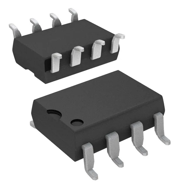
8-Pin DIP (300 Mil)
Single
Dual
Channel
Channel
Package
Package
[1]
HCPL-2200
HCPL-2201
HCPL-2202
HCPL-2231
[1]
HCPL-2219
HCPL-2211
HCPL-2212
HCPL-2232
Small-Outline
SO-8
Single
Channel
Package
HCPL-0201
Widebody
(400 Mil)
Single
Channel
Package
HCNW2201
HCPL-0211
HCNW2211
Notes:
1. HCPL-2200/2219 devices include output enable/disable functionality.
2. Minimum CMR of 10 kV/µs with VCM = 1000 V can be achieved with input current, IF, of 5 mA.
2
Hermetic
Single and Dual
Channel
Packages
HCPL-52XX
HCPL-62XX
�Ordering Information
HCPL-2200, HCPL-2219 are UL Recognized with 3750 Vrms for 1 minute per UL1577 and are approved
under CSA Component Acceptance Notice #5, File CA 88324.
Option
Part
RoHS
non RoHS
Number Compliant Compliant
-000E
no option
HCPL-2200 -300E
-300
-500E
-500
-000E
no option
-300E
-300
HCPL-2219 -500E
-500
-060E
-060
-360E
-360
-560E
-560
Package
300 mil DIP-8
Surface
Mount
Gull
Wing
Tape
& Reel
X
X
X
X
X
X
X
X
X
X
X
X
X
X
X
300 mil DIP-8
UL 5000 Vrms/
1 Minute rating
IEC/EN/DIN
EN 60747-5-2 Quantity
50 per tube
50 per tube
1000 per reel
50 per tube
50 per tube
1000 per reel
X
50 per tube
X
50 per tube
X
1000 per reel
To order, choose a part number from the part number column and combine with the desired option from
the option column to form an order entry.
Example 1:
HCPL-2219-560E to order product of 300 mil DIP Gull Wing Surface Mount package in Tape and Reel
packaging with IEC/EN/DIN EN 60747-5-2 Safety Approval and RoHS compliant.
Example 2:
HCPL-2200 to order product of 300 mil DIP package in Tube packaging and non RoHS compliant.
Option datasheets are available. Contact your Avago sales representative or authorized distributor for
information.
Remarks: The notation ‘#XXX’ is used for existing products, while (new) products launched since July 15,
2001 and RoHS compliant will use ‘–XXXE.’
Schematic
ICC
8
IF
+
VF
IO
2
7
IE
–
6
3
SHIELD
3
5
VCC
VO
VE
GND
�Package Outline Drawings
8-Pin DIP Package
7.62 ± 0.25
(0.300 ± 0.010)
9.65 ± 0.25
(0.380 ± 0.010)
8
TYPE NUMBER
7
6
5
6.35 ± 0.25
(0.250 ± 0.010)
OPTION CODE*
DATE CODE
A XXXXZ
YYWW RU
1
2
3
4
UL
RECOGNITION
1.78 (0.070) MAX.
1.19 (0.047) MAX.
+ 0.076
0.254 - 0.051
+ 0.003)
(0.010 - 0.002)
5° TYP.
3.56 ± 0.13
(0.140 ± 0.005)
4.70 (0.185) MAX.
0.51 (0.020) MIN.
DIMENSIONS IN MILLIMETERS AND (INCHES).
*MARKING CODE LETTER FOR OPTION NUMBERS.
"V" = OPTION 060
OPTION NUMBERS 300 AND 500 NOT MARKED.
2.92 (0.115) MIN.
0.65 (0.025) MAX.
1.080 ± 0.320
(0.043 ± 0.013)
NOTE: FLOATING LEAD PROTRUSION IS 0.25 mm (10 mils) MAX.
2.54 ± 0.25
(0.100 ± 0.010)
8-Pin DIP Package with Gull Wing Surface Mount Option 300
LAND PATTERN RECOMMENDATION
9.65 ± 0.25
(0.380 ± 0.010)
8
7
6
1.016 (0.040)
5
6.350 ± 0.25
(0.250 ± 0.010)
1
2
3
10.9 (0.430)
4
1.27 (0.050)
1.19
(0.047)
MAX.
1.780
(0.070)
MAX.
9.65 ± 0.25
(0.380 ± 0.010)
7.62 ± 0.25
(0.300 ± 0.010)
3.56 ± 0.13
(0.140 ± 0.005)
1.080 ± 0.320
(0.043 ± 0.013)
0.635 ± 0.25
(0.025 ± 0.010)
0.635 ± 0.130
2.54
(0.025 ± 0.005)
(0.100)
BSC
DIMENSIONS IN MILLIMETERS (INCHES).
LEAD COPLANARITY = 0.10 mm (0.004 INCHES).
NOTE: FLOATING LEAD PROTRUSION IS 0.25 mm (10 mils) MAX.
4
2.0 (0.080)
+ 0.076
0.254 - 0.051
+ 0.003)
(0.010 - 0.002)
12° NOM.
�Solder Reflow Thermal Profile
Regulatory Information
The HCPL-2200/2219 have been
approved by the following
organizations:
300
TEMPERATURE (°C)
PREHEATING RATE 3°C + 1°C/–0.5°C/SEC.
REFLOW HEATING RATE 2.5°C ± 0.5°C/SEC.
PEAK
TEMP.
245°C
PEAK
TEMP.
240°C
PEAK
TEMP.
230°C
200
2.5°C ± 0.5°C/SEC.
30
SEC.
160°C
150°C
140°C
30
SEC.
3°C + 1°C/–0.5°C
100
PREHEATING TIME
150°C, 90 + 30 SEC.
50 SEC.
TIGHT
TYPICAL
LOOSE
ROOM
TEMPERATURE
0
0
50
100
150
200
TIME (SECONDS)
Note: Non-halide flux should be used.
Recommended Pb-Free IR Profile
tp
Tp
TL
TEMPERATURE
UL
Recognized under UL 1577,
Component Recognition Program,
File E55361.
SOLDERING
TIME
200°C
Tsmax
TIME WITHIN 5 °C of ACTUAL
PEAK TEMPERATURE
CSA
Approved under CSA Component
Acceptance Notice #5, File CA
88324.
250
IEC/EN/DIN EN 60747-5-2
Approved under:
IEC 60747-5-2:1997 + A1:2002
EN 60747-5-2:2001 + A1:2002
DIN EN 60747-5-2 (VDE 0884
Teil 2):2003-01.
(Option 060 only)
20-40 SEC.
260 +0/-5 °C
217 °C
RAMP-UP
3 °C/SEC. MAX.
150 - 200 °C
RAMP-DOWN
6 °C/SEC. MAX.
Tsmin
ts
PREHEAT
60 to 180 SEC.
tL
60 to 150 SEC.
25
t 25 °C to PEAK
TIME
NOTES:
THE TIME FROM 25 °C to PEAK TEMPERATURE = 8 MINUTES MAX.
Tsmax = 200 °C, Tsmin = 150 °C
Note: Non-halide flux should be used.
Insulation and Safety Related Specifications
Parameter
Min. External Air Gap
(External Clearance)
Min. External
Tracking Path
(External Creepage)
Minimum Internal
Plastic Gap
(Internal Clearance)
Tracking Resistance
(Comparative
Tracking Index)
Isolation Group
Symbol
L(IO1)
Value
7.1
Units
mm
L(IO2)
7.4
mm
0.08
mm
200
V
CTI
IIIa
Conditions
Measured from input terminals to output terminals,
shortest distance through air.
Measured from input terminals to output terminals,
shortest distance path along body.
Through insulation distance, conductor to conductor,
usually the direct distance between the photoemitter
and photodetector inside the optocoupler cavity.
DIN IEC 112/VDE 0303 Part 1
Material Group (DIN VDE 0110, 1/89, Table 1)
Option 300 – surface mount classification is Class A in accordance with CECC 00802.
5
�IEC/EN/DIN EN 60747-5-2 Insulation Related Characteristics (HCPL-2219 OPTION 060 ONLY)
Description
Symbol
Installation classification per DIN VDE 0110/1.89, Table 1
for rated mains voltage ≤300 V rms
Units
I-IV
for rated mains voltage ≤450 V rms
I-III
Climatic Classification
55/85/21
Pollution Degree (DIN VDE 0110/1.89)
Maximum Working Insulation Voltage
Characteristic
2
VIORM
630
V peak
Input to Output Test Voltage, Method b*
VIORM x 1.875 = VPR, 100% Production Test with tm = 1 sec,
Partial Discharge < 5 pC
VPR
1181
V peak
Input to Output Test Voltage, Method a*
VIORM x 1.5 = VPR, Type and sample test,
tm = 60 sec, Partial Discharge < 5 pC
VPR
945
V peak
VIOTM
6000
V peak
TS
IS,INPUT
PS,OUTPUT
175
230
600
°C
mA
mW
RS
≥109
Ω
Highest Allowable Overvoltage*
(Transient Overvoltage, tini = 10 sec)
Safety Limiting Values
(Maximum values allowed in the event of a failure,
also see Figure 12, Thermal Derating curve.)
Case Temperature
Input Current
Output Power
Insulation Resistance at TS, VIO = 500 V
*Refer to the front of the optocoupler section of the current catalog, under Product Safety Regulations section, IEC/EN/DIN EN 60747-5-2, for a
detailed description.
Note: Isolation characteristics are guaranteed only within the safety maximum ratings which must be ensured by protective circuits in application.
6
�Absolute Maximum Ratings
(No Derating Required up to 70°C)
Parameter
Storage Temperature
Operating Temperature
Average Forward Input Current
Peak Transient Input Current
(≤1 µs Pulse Width, 300 pps)
Reverse Input Voltage
Average Output Current
Supply Voltage
Three State Enable Voltage
Output Voltage
Total Package Power Dissipation
Lead Solder Temperature
Solder Reflow Temperature Profile
Recommended Operating Conditions
Parameter
Symbol
Power Supply Voltage
VCC
Enable Voltage High
VEH
Enable Voltage Low
VEL
Forward Input Current
IF(ON)
Forward Input Current
IF(OFF)
Operating Temperature
TA
Fan Out
N
Symbol
TS
TA
IF(AVG)
IF(TRAN)
Min.
-55
-40
Units
°C
°C
mA
A
VR
5
V
IO
25
mA
VCC
0
20
V
VE
-0.5
20
V
VO
-0.5
20
V
PT
210
mW
260°C for 10 sec., 1.6 mm below seating plane
See Package Outline Drawings section
Min.
4.5
2.0
0
1.6*
–
0
Max.
20
20
0.8
5
0.1
85[1]
4
Units
V
V
V
mA
mA
°C
TTL Loads
*The initial switching threshold is 1.6 mA or less. It is recommended that 2.2 mA be used to permit
at least a 20% CTR degradation guardband.
7
Max.
125
85
10
1.0
Note
1
1
�Electrical Specifications
For 0°C ≤ TA[1] ≤ 85°C, 4.5 V ≤ VCC ≤ 20 V, 1.6 mA ≤ IF(ON) ≤ 5 mA, 2.0 V ≤ VEH ≤ 20 V, 0.0 V ≤ VEL ≤ 0.8 V, 0 mA ≤ IF(OFF) ≤ 0.1 mA.
All Typicals at TA = 25°C, VCC = 5 V, IF(ON) = 3 mA unless otherwise specified. See Note 7.
Parameter
Logic Low
Output Voltage
Logic High
Output Voltage
Output Leakage
Current (VOUT > VCC)
Sym.
VOL
Min.
Typ.
VOH
2.4
*
Logic High Enable
Voltage
Logic Low Enable
Voltage
Logic High Enable
Current
VEH
Logic High Supply
Current
High Impedance
State Output Current
Logic Low Short
Circuit Output
Current
Logic High Short
Circuit Output
Current
Input Current
Hysteresis
Input Forward
Voltage
Input Reverse
Breakdown Voltage
Input Diode
Temperature
Coefficient
Input Capacitance
8
Test Conditions
IOL = 6.4 mA (4 TTL Loads)
V
IOH = -2.6 mA
100
µA
VO = 5.5 V
500
µA
V
VO = 20 V
VEL
0.8
V
IEH
20
100
250
-0.32
µA
µA
µA
mA
VEN = 2.7 V
VEN = 5.5 V
VEN = 20 V
VEN = 0.4 V
4.5
6.0
mA
VCC = 5.5 V
5.25
7.5
mA
VCC = 20 V
2.7
4.5
mA
VCC = 5.5 V
3.1
6.0
mA
VCC = 20 V
IOZL
-20
µA
VO = 0.4 V
IOZH
20
100
500
µA
µA
µA
VO = 2.4 V
VO = 5.5 V
VO = 20 V
25
mA
VO = VCC = 5.5 V
40
mA
VO = VCC = 20 V
-10
mA
VCC = 5.5 V
-25
mA
VCC = 20 V
mA
VCC = 5 V
V
TA = 25°C
V
IR = 10 µA
IOHH
2.0
0.004
Logic Low Enable
Current
Logic Low Supply
Current
Max. Units
0.5
V
IEL
ICCL
ICCH
IOSL
IOSH
IHYS
0.12
VF
1.5
BVR
5
∆VF
∆TA
-1.7
CIN
60
1.7
1.75
*VOH = VCC - 2.1 V
Note
2
IF = 5 mA
VCC = 4.5 V
IF = 0 mA
IO = Open
VE = Don’t Care
IF = 5 mA
IO = Open
VE = Don’t Care
VEN = 2 V,
IF = 5 mA
VEN = 2 V,
IF = 5 mA
IF = 0 mA
2
IF = 5 mA,
VO = GND
2
3
IF = 5 mA
mV/°C IF = 5 mA
pF
Fig.
1
f = 1 MHz, VF = 0 V, Pins 2 and 3
4
�Switching Specifications (AC)
For 0°C ≤ TA[1] ≤ 85°C, 4.5 V ≤ VCC ≤ 20 V, 1.6 mA ≤ IF(ON) ≤ 5 mA, 0.0 mA ≤ IF(OFF) ≤ 0.1 mA.
All Typicals at TA = 25°C, VCC = 5 V, IF(ON) = 3 mA unless otherwise specified.
Parameter
Propagation Delay Time to
Logic Low Output Level
Sym.
tPHL
Propagation Delay Time to
Logic High Output Level
tPLH
Output Enable Time to
Logic High
Output Enable Time to
Logic Low
Output Disable Time from
Logic High
Output Disable Time from
Logic Low
Output Rise Time (10-90%)
Output Fall Time (90-10%)
tPZH
160
170
115
25
tPZL
Parameter
Logic High
Common Mode
Transient
Immunity
Logic Low
Common Mode
Transient
Immunity
Sym.
|CMH|
|CML|
Min.
Typ.
210
Max. Units
ns
300
ns
300
Test Conditions
Without Peaking Capacitor
Fig.
5, 6
Note
4, 5
With Peaking Capacitor
Without Peaking Capacitor
With Peaking Capacitor
5, 6
4, 5
ns
7, 9
28
ns
7, 8
tPHZ
105
ns
7, 9
tPLZ
60
ns
7, 8
tr
tf
55
15
ns
ns
5, 10
5, 10
Device
Min.
Units
HCPL-2200
1,000
V/µs
HCPL-2219
2,500
V/µs
Test Conditions
IF = 1.6 mA
|VCM| = 50 V
VCC = 5 V
TA = 25°C
|VCM| = 400 V
HCPL-2200
1,000
V/µs
|VCM| = 50 V
HCPL-2219
2,500
V/µs
|VCM| = 400 V
VF = 0 V
VCC = 5 V
TA = 25°C
Fig.
11
Note
6
11
6
Package Characteristics
Parameter
Input-Output Momentary
Withstand Voltage*
Input-Output Resistance
Input-Output Capacitance
Sym.
VISO
RI-O
CI-O
Min.
3750
Typ.
1012
0.6
Max.
Units
V rms
Ω
pF
Test Conditions
RH ≤50%, t = 1 min.,
TA = 25°C
VI-O = 500 VDC
f = 1 MHz, VI-O = 0 VDC
Fig.
Note
3, 8
3
3
*The Input-Output Momentary Withstand Voltage is a dielectric voltage rating that should not be interpreted as an input-output continuous voltage rating. For
the continuous voltage rating refer to the IEC/EN/DIN EN 60747-5-2 Insulation Characteristics Table (if applicable), your equipment level safety specification
or Avago Application Note 1074 entitled “Optocoupler Input-Output Endurance Voltage,” publication number 5963-2203E.
9
�Notes:
1. Derate total package power dissipation, PT,
linearly above 70°C free air temperature at a
rate of 4.5 mW/°C.
2. Duration of output short circuit time should
not exceed 10 ms.
3. Device considered a two-terminal device:
pins 1, 2, 3, and 4 shorted together and pins
5, 6, 7, and 8 shorted together.
4. The tPLH propagation delay is measured
from the 50% point on the leading edge of
the input pulse to the 1.3 V point on the
leading edge of the output pulse. The tPHL
propagation delay is measured from the
50% point on the trailing edge of the input
pulse to the 1.3 V point on the trailing edge
of the output pulse.
5. When the peaking capacitor is omitted,
propagation delay times may increase by
100 ns.
6. CML is the maximum rate of rise of the
common mode voltage that can be
sustained with the output voltage in the
logic low state (VO < 0.8 V). CMH is the
maximum rate of fall of the common mode
voltage that can be sustained with the
output voltage in the logic high state
(VO > 2.0 V).
VOL – LOW LEVEL OUTPUT VOLTAGE – V
IOH – HIGH LEVEL OUTPUT CURRENT – mA
VCC = 4.5 V
IF = 0 mA
VO = 6.4 mA
0.9
0.8
0.7
0.6
0.5
0.4
0.3
0.2
0.1
0
-60 -40 -20
0
20
40
60
80 100
0
5
VCC = 4.5 V
IF = 5 mA
-1
-2
VO = 2.7 V
-3
-4
-5
VO = 2.4 V
-6
-7
-8
-60 -40 -20
TA – TEMPERATURE – °C
Figure 1. Typical logic low output voltage vs.
temperature.
0
INPUT
MONITORING
NODE
IF – FORWARD CURRENT – mA
R1
TA = 25 °C
10
60
3
IOH = -2.6 mA
2
1
IOL = 6.4 mA
80 100
0
OUTPUT VO
MONITORING
NODE
HCPL-2200
1
VCC 8
2
7
3
6
GND 5
5 kΩ
IF (ON)
50 % IF (ON)
0 mA
INPUT IF
1.4
1.5
Figure 4. Typical input diode forward
characteristic.
D3
D4
ALL DIODES ARE 1N916 OR 1N3064.
1.3
619 Ω
D2
C2 =
15 pF
0.1
1.2
5V
D1
2.15 kΩ 1.10 kΩ 681 Ω
RI
5 mA
IF (ON) 1.6 mA 3 mA
VF – FORWARD VOLTAGE – V
tPLH
1.5
2.0
Figure 3. Output voltage vs. forward input
current.
THE PROBE AND JIG CAPACITANCES
ARE INCLUDED IN C1 AND C2.
0.01
1.0
VCC
4
C1 =
120 pF
IF
+
VF
–
0.5
IF – INPUT CURRENT – mA
1.0
0.001
1.1
10
40
4
0
Figure 2. Typical logic high output current vs.
temperature.
IF
100
20
VCC = 4.5 V
TA = 25 °C
TA – TEMPERATURE – °C
PULSE GEN.
tr = tf = 5 ns
f = 100 kHz
10 % DUTY
CYCLE
VO = 5 V
1000
VO – OUTPUT VOLTAGE – V
1.0
7. Use of a 0.1 µF bypass capacitor connected
between pins 5 and 8 is recommended.
8. In accordance with UL1577, each
optocoupler is proof tested by applying an
insulation test voltage ≥4500 V rms for one
second (leakage detection current limit, II-O
≤5 µA). This test is performed before the
100% production test for partial discharge
(Method b) shown in the IEC/EN/DIN EN
60747-5-2 Insulation Characteristics Table, if
applicable.
tPHL
OUTPUT
VO
Figure 5. Test circuit for tPLH, tPHL, tr, and tf.
VOH
1.3 V
VOL
�tP – PROPAGATION DELAY – ns
250
200
VCC = 5 V
C1 (120 pF) PEAKING
CAPACITOR IS USED.
SEE FIGURE 5.
CL= 15 pF INCLUDING PROBE
PULSE
AND JIG CAPACITANCES.
GENERATOR
VCC
ZO = 50 Ω
tr = tf = 5 ns
VO
HCPL-2200
IF (mA)
5
3
1.6
150
1.6
3
5
tPHL
20
40
60
619 Ω
D1
IF
tPLH
0
S1
VCC 8
1
100
50
-60 -40 -20
+5 V
2
7
3
6
4
GND 5
D2
CL
5 kΩ
D3
INPUT VC
MONITORING
NODE
80 100
TA – TEMPERATURE – °C
D4
S2
D1-4 ARE 1N916 OR 1N3064.
Figure 6. Typical propagation delays vs.
temperature.
INPUT
VE
tPZL
3.0 V
1.3 V
0V
S1 AND
S2 CLOSED
tPLZ
OUTPUT S1 CLOSED
VO
S2 OPEN
tPZH
OUTPUT
VO
S1 OPEN
S2 CLOSED
1.3 V
0.5 V
VOL
0.5 V
VOH
≈1.5 V
S1 AND
S2 CLOSED
1.3 V
0V
tPHZ
VCC
20 V
CL = 15 pF
80
4.5 V
tPLZ
60
20 V
40
4.5 V
tPZL
20
0
-60 -40 -20
0
20
40
60
TA – TEMPERATURE – °C
Figure 8. Typical logic low enable
propagation delay vs. temperature.
11
80 100
200
120
CL = 15 pF
VCC
150
20 V
tPHZ
4.5 V
100
20 V
50
4.5 V
tPZH
tr, tf – RISE, FALL TIME – ns
100
tP – ENABLE PROPAGATION DELAY – ns
Tp – ENABLE PROPAGATION DELAY – ns
Figure 7. Test circuit for tPHZ, tPZH, tPLZ, and tPZL.
VCC = 5 V
C2 = 15 pF
100
80
60
tr
40
20
tf
0
-60 -40 -20
0
20
40
60
TA – TEMPERATURE – °C
Figure 9. Typical logic high enable
propagation delay vs. temperature.
80 100
0
-60 -40 -20
0
20
40
60
TA – TEMPERATURE – °C
Figure 10. Typical rise, fall time vs.
temperature.
80 100
�OUTPUT VO
MONITORING
NODE
VCC 8
A
1
B
2
7
3
6
RIN
VFF
4
GND
OUTPUT POWER – PS, INPUT CURRENT – IS
VCC
HCPL-2200
0.1 µF
BYPASS
5
VCM
–
PULSE GENERATOR +
50 V
VCM
0V
VOH
PS (mW)
700
IS (mA)
600
500
400
300
200
100
0
0
25
50
75 100 125 150 175 200
TS – CASE TEMPERATURE – °C
SWITCH AT A: IF = 1.6 mA
VO (MIN.)*
SWITCH AT B: IF = 0 mA
VO (MAX.)*
OUTPUT
VO
HCPL-2219 OPTION 060 ONLY
800
Figure 12. Thermal derating curve,
dependence of safety limiting value with case
temperature per IEC/EN/DIN EN 60747-5-2.
VOL
* SEE NOTE 6.
Figure 11. Test circuit for common mode transient immunity and typical waveforms.
VCC1
(+5 V)
VCC1
(+5 V)
120 pF
HCPL-2200
1.1
kΩ
DATA
INPUT
TTL OR
LSTTL
TOTEM
POLE
OUTPUT
GATE
VCC
1
2
7
3
6
GND
4
HCPL-2200
1.1
kΩ
DATA
OUTPUT
8
5
DATA
INPUT
TOTEM
POLE
OUTPUT
GATE
1
2
VCC (+5 V)
TTL OR
LSTTL
RL
1.1 K
2.37 K
3.83 K
5.11 K
2
120 pF (OPTIONAL*)
1.1
kΩ
HCPL-2200
DATA
INPUT
5
Figure 14. LSTTL to CMOS interface circuit.
Figure 13. Recommended LSTTL to LSTTL circuit.
1.1 kΩ
CMOS
6
GND
4
VCC2
5V
10 V
15 V
20 V
RL
8
7
3
TTL OR
LSTTL
1
VCC1 (+5 V)
VCC
1
2
UP TO 16
LSTTL
LOADS
OR 4 TTL
LOADS
VCC2
(4.5 TO 20 V)
120 pF (OPTIONAL*)
VCC2
(+5 V)
1
VCC 8
2
7
HCPL-2200
1
VCC
2
8
7
4.7 kΩ
D1
3
4
6
GND
5
DATA
INPUT
OPEN
COLLECTOR
GATE
3
TTL OR
LSTTL
4
6
GND
5
D1 (1N4150) REQUIRED FOR
ACTIVE PULL-UP DRIVER.
Figure 15. Recommended LED drive circuit.
Figure 16. Series LED drive with open collector gate (4.7 kΩ resistor
dhunts IOH from the LED).
*The 120 pF capacitor may be omitted in applications where 500 ns propagation delay is sufficient.
12
DATA
OUTPUT
�For product information and a complete list of distributors, please go to our website:
www.avagotech.com
Avago, Avago Technologies, and the A logo are trademarks of Avago Technologies Limited in the United States and other countries.
Data subject to change. Copyright © 2007 Avago Technologies Limited. All rights reserved. Obsoletes 5989-2124EN
AV01-0557EN July 5, 2007
�


 工商网监
湘ICP备2023018690号
工商网监
湘ICP备2023018690号