HCPL-2730/0730/2731/0731
Dual Channel Low Input Current, High Gain Optocouplers
Data Sheet
Lead (Pb) Free
RoHS 6 fully
compliant
RoHS 6 fully compliant options available;
-xxxE denotes a lead-free product
Description
These dual channel optocouplers contain a separated
pair of GaAsP light emitting diodes optically coupled
to a pair of integrated high gain photo detectors. They
provide extremely high current transfer ratio and excellent input-output common mode transient immunity. A
separate pin for the photodiodes and first gain stages
(VCC) permits lower output saturation voltage and higher
speed operation than possible with conventional photo
darlington type optocouplers. In addition, VCC may be as
low as 1.6 V without adversely affecting the parametric
performance.
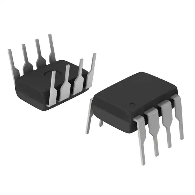
These dual channel optocouplers are available in an 8Pin DIP and in an industry standard SO-8 package. The
following is a cross reference table listing the 8-Pin DIP
part number and the electrically equivalent SOIC-8 part
number.
8-Pin DIP
HCPL-2730
HCPL-2731
SO-8
HCPL-0730
HCPL-0731
The SO-8 does not require “through holes” in a PCB. This
package occupies approximately one-third the footprint
area of the standard dual-in-line package. The lead profile
is designed to be compatible with standard surface mount
processes.
Functional Diagram
ANODE 1 1
8 VCC
CATHODE 1 2
7 VO1
CATHODE 2 3
6 VO2
ANODE 2 4
TRUTH TABLE
LED
VO
ON
LOW
OFF
HIGH
Features
• High current transfer ratio – 1800% typical
• Low input current requirements – 0.5 mA
• Low output saturation voltage – 0.1 V
• High density packaging
• Performance guaranteed over temperature 0°C to 70°C
• LSTTL compatible
• High output current – 60 mA
• Safety approval:
UL recognized – 3750 V rms for 1 minute and
5000 V rms* for 1 minute
CSA approved
• Available in 8 pin DIP and SO-8 footprint
• MIL-PRF-38534 hermetic version available
(HCPL-5730/5731)
• Surface mount gull wing option available for 8-pin DIP
(Option 300)
Applications
• Digital logic ground isolation
• Telephone ring detector
• Level shifting
• EIA RS-232C line receiver
• Polarity sensing
• Low input current line receiver – long line or party line
• Microprocessor bus isolation
• Current loop receiver
• Line voltage status indicator – low input power dissipation
*5000 V rms/1 minute withstand voltage rating is for Option 020
(HCPL-2730, HCLP-2731) products only.
5 GND
A 0.1 µF bypass capacitor connected between pins 5
and 8 is recommended.
CAUTION: It is advised that normal static precautions be taken in handling and assembly of this component to prevent damage
HCPL-2730 Functional Diagram
and/or degradation which may be induced by ESD.
�Guaranteed operation at low input currents
and the high current transfer ratio (CTR) reduce
the magnitude and effects of CTR degradation.
The outstanding high temperature performance of this split
Darlington type output amplifier results from the inclusion
of an integrated emitter-base bypass resistor which shunts
photodiode and first stage leakage currents to ground.
The HCPL-2731/0731 have a 400% minimum CTR at an input
current of only 0.5 mA making it ideal for use in low input current applications such as MOS, CMOS, and low power logic
interfacing or RS232C data transmission systems. In addi
tion, the high CTR and high output current capability make
this device extremely useful in applications where a high
fanout is required. Compatibility with high voltage CMOS
logic systems is guaranteed by the 18 V VCC and VO specifica
tions and by testing output high leakage (IOH) at 18 V.
The HCPL-2730/0730 are specified at an input current of 1.6
mA and have a 7 V VCC and VO rating. The 300% minimum
CTR allows TTL to TTL interfacing at this input current.
Important specifications such as CTR, leakage current, and output saturation voltage are guaranteed
over the 0°C to 70°C temperature range to allow
trouble-free system operation. Selection for lower input currents down to 250 µA is available upon request.
Selection Guide
Widebody
Package
8-Pin DIP (300 Mil)
Small Outline SO-8
(400 mil)
Dual
Single
Dual
Minimum
Absolute
Single
Channel
Channel
Channel
Single
Input ON
Maxi-
Channel
Package
Package
Package
Channel
Current
Minimum
mum
Package
HCPL-
HCPL-
HCPL-
Package
(IF)
CTR
VCC
6N139[1]
2731
0701[1]
0731
HCNW139[1]
0.5 mA
400%
18 V
6N138
2730
0700
0730
HCNW138
1.6 mA
300%
7V
40 µA
800%
18 V
[1]
HCPL-4701
[1]
4731
[1]
[1]
070A
[1]
073A
[1]
[1]
0.5 mA
300%
20 V
Note:
1. Technical data are on separate Avago publications.
�
Hermetic
Single and
Dual
Channel
Packages
HCPL-
5701[1]
5700[1]
5731[1]
5730[1]
�Ordering Information
HCPL-2730, HCPL-2731, HCPL-0730 and HCPL-0731 are UL Recognized with 3750 Vrms for 1 minute per UL1577 and
are approved under CSA Component Acceptance Notice #5, File CA 88324.
Option
Part number
HCPL-2730
HCPL-2731
HCPL-0730
HCPL-0731
RoHS
Compliant
Non RoHS
Compliant
-000E
No option
-300E
-300
-500E
-500
-020E
-020
-320E
-320
X
X
-520E
-520
X
X
-060E
-060
-360E
-360
X
X
-560E
-560
X
X
-000E
No option
-500E
-500
-060E
-060
-560E
-560
Package
Surface Gull
Mount Wing
Tape
& Reel
UL 5000 Vrms/
1 Minute rating
IEC/EN/DIN
EN 60747-5-2 Quantity
50 per tube
300mil
DIP-8
X
X
X
X
50 per tube
X
X
X
1000 per reel
X
50 per tube
X
50 per tube
X
1000 per reel
X
50 per tube
X
50 per tube
X
1000 per reel
100 per tube
SO-8
X
X
X
X
X
X
1500 per reel
X
100 per tube
X
1500 per reel
To order, choose a part number from the part number column and combine with the desired option from the option
column to form an order entry.
Example 1:
HCPL-2730-520E to order product of 300mil DIP Gull Wing Surface Mount package in Tape and Reel packaging
with UL 5kVrms 1minute rating in RoHS compliant.
Example 2:
HCPL-2730 to order product of 300mil DIP package in tube packaging and non RoHS compliant.
Option datasheets are available. Contact your Avago sales representative or authorized distributor for information.
Remarks: The notation ‘#XXX’ is used for existing products, while (new) products launched since 15th July 2001 and
RoHS compliant option will use ‘-XXXE‘.
�
�Schematic
1
+
I CC
I F1
8
VCC
VF1
–
I O1
2
3
–
7
VO1
I F2
I O2
6
VF2
VO2
+
4
5
HCPL-2731/0731 SHIELD
GND
USE OF A 0.1 µF BYPASS CAPACITOR CONNECTED
BETWEEN PINS 5 AND 8 IS RECOMMENDED (SEE NOTE 8)
HCPL-2730 Schematic
Package Outline Drawings
8-Pin DIP Package (HCPL-2731/HCPL-2730)
7.62 ± 0.25
(0.300 ± 0.010)
9.65 ± 0.25
(0.380 ± 0.010)
TYPE NUMBER
8
7
6
5
OPTION CODE*
DATE CODE
A XXXXZ
6.35 ± 0.25
(0.250 ± 0.010)
YYWW RU
1
1.19 (0.047) MAX.
2
3
4
UL
RECOGNITION
1.78 (0.070) MAX.
5° TYP.
3.56 ± 0.13
(0.140 ± 0.005)
4.70 (0.185) MAX.
+ 0.076
0.254 - 0.051
+ 0.003)
(0.010 - 0.002)
0.51 (0.020) MIN.
2.92 (0.115) MIN.
1.080 ± 0.320
(0.043 ± 0.013)
�
0.65 (0.025) MAX.
2.54 ± 0.25
(0.100 ± 0.010)
DIMENSIONS IN MILLIMETERS AND (INCHES).
*MARKING CODE LETTER FOR OPTION NUMBERS
"L" = OPTION 020
OPTION NUMBERS 300 AND 500 NOT MARKED.
NOTE: FLOATING LEAD PROTRUSION IS 0.25 mm (10 mils) MAX.
�8-Pin DIP Package with Gull Wing Surface Mount Option 300 (HCPL-2731/HCPL-2730)
LAND PATTERN RECOMMENDATION
9.65 ± 0.25
(0.380 ± 0.010)
6
7
8
1.016 (0.040)
5
6.350 ± 0.25
(0.250 ± 0.010)
1
3
2
10.9 (0.430)
4
2.0 (0.080)
1.27 (0.050)
9.65 ± 0.25
(0.380 ± 0.010)
1.780
(0.070)
MAX.
1.19
(0.047)
MAX.
7.62 ± 0.25
(0.300 ± 0.010)
+ 0.076
0.254 - 0.051
+ 0.003)
(0.010 - 0.002)
3.56 ± 0.13
(0.140 ± 0.005)
1.080 ± 0.320
(0.043 ± 0.013)
0.635 ± 0.25
(0.025 ± 0.010)
0.635 ± 0.130
2.54
(0.025 ± 0.005)
(0.100)
BSC
DIMENSIONS IN MILLIMETERS (INCHES).
LEAD COPLANARITY = 0.10 mm (0.004 INCHES).
12° NOM.
NOTE: FLOATING LEAD PROTRUSION IS 0.25 mm (10 mils) MAX.
Small Outline SO-8 Package (HCPL-0731/HCPL-0730)
LAND PATTERN RECOMMENDATION
8
7
6
5
XXX
YWW
3.937 ± 0.127
(0.155 ± 0.005)
5.994 ± 0.203
(0.236 ± 0.008)
TYPE NUMBER
(LAST 3 DIGITS)
7.49 (0.295)
DATE CODE
PIN ONE 1
2
3
0.406 ± 0.076
(0.016 ± 0.003)
4
1.9 (0.075)
1.270 BSC
(0.050)
7°
* 5.080 ± 0.127
(0.200 ± 0.005)
3.175 ± 0.127
(0.125 ± 0.005)
0.64 (0.025)
45° X
0.432
(0.017)
0.228 ± 0.025
(0.009 ± 0.001)
1.524
(0.060)
0.203 ± 0.102
(0.008 ± 0.004)
* TOTAL PACKAGE LENGTH (INCLUSIVE OF MOLD FLASH)
5.207 ± 0.254 (0.205 ± 0.010)
DIMENSIONS IN MILLIMETERS (INCHES).
LEAD COPLANARITY = 0.10 mm (0.004 INCHES) MAX.
�
0.305 MIN.
(0.012)
NOTE: FLOATING LEAD PROTRUSION IS 0.15 mm (6 mils) MAX.
�Solder Reflow Thermal Profile
TEMPERATURE (°C)
300
PREHEATING RATE 3°C + 1°C/–0.5°C/SEC.
REFLOW HEATING RATE 2.5°C ± 0.5°C/SEC.
200
PEAK
TEMP.
245°C
PEAK
TEMP.
240°C
2.5°C ± 0.5°C/SEC.
30
SEC.
3°C + 1°C/–0.5°C
100
PREHEATING TIME
150°C, 90 + 30 SEC.
50 SEC.
TIGHT
TYPICAL
LOOSE
ROOM
TEMPERATURE
0
0
50
100
150
200
TIME (SECONDS)
Note: Non-halide flux should be used.
Recommended Pb-Free IR Profile
tp
TEMPERATURE
Tp
TL
Tsmax
217 °C
260 +0/-5 °C
RAMP-UP
3 °C/SEC. MAX.
150 - 200 °C
TIME WITHIN 5 °C of ACTUAL
PEAK TEMPERATURE
20-40 SEC.
RAMP-DOWN
6 °C/SEC. MAX.
Tsmin
ts
PREHEAT
60 to 180 SEC.
25
tL
60 to 150 SEC.
t 25 °C to PEAK
TIME
NOTES:
THE TIME FROM 25 °C to PEAK TEMPERATURE = 8 MINUTES MAX.
Tsmax = 200 °C, Tsmin = 150 °C
Note: Non-halide flux should be used.
�
UL
Recognized under UL 1577, Component Recognition Program, File
E55361.
PEAK
TEMP.
230°C
SOLDERING
TIME
200°C
30
SEC.
160°C
150°C
140°C
Regulatory Information
The HCPL-2731/2730 have been approved by the following organizations:
250
CSA
Approved under CSA Component
Acceptance Notice #5, File CA
88324.
IEC/EN/DIN EN 60747-5-2
Approved under
IEC 60747-5-2:1997 + A1:2002
EN 60747-5-2:2001 + A1:2002
DIN EN 60747-5-2 (VDE 0884
Teil 2):2003-01
(Option 060 only)
�Insulation Related Specifications (HCPL-2731/2730/0731/0730)
8-Pin DIP
(300 Mil)
SO-8
Parameter
Symbol
Value
Value
Units
Conditions
Minimum External Air
L(101)
7.1
4.9
mm
Gap (External Clearance)
Measured from input terminals to output
terminals, shortest distance through air.
Minimum External
L(102)
7.4
4.8
mm
Tracking (External
Creepage)
Measured from input terminals to
output terminals, shortest distance
path along body.
Minimum Internal Plastic
0.08
0.08
mm
Gap (Internal Clearance)
Through insulation distance, conductor
to conductor, usually the direct distance
between the photoemitter and photode
tector inside the optocoupler cavity.
Tracking Resistance
(Comparative Tracking
Index)
DIN IEC 112/ VDE 0303 Part 1
CTI
Isolation Group
200
200
Volts
IIIa
IIIa
Material Group DIN VDE 0110
Option 300 – surface mount classification is Class A in accordance with CECC 00802.
IEC/EN/DIN EN 60747-5-2 Insulation Related Characteristics
Description
Symbol
Characteristic
Installation Classification per DIN VDE 0110/1.89, Table 1
for rated mains voltage ≤600 V rms
for rated mains voltage ≤1000 V rms
I-III
Climatic Classification
55/100/21
Pollution Degree (DIN VDE 0110/1.89)
2
Units
I-IV
Maximum Working Insulation Voltage
VIORM
1414
V peak
Input to Output Test Voltage, Method b*
VPR = 1.875 x VIORM, 100% Production Test with tP = 1 sec,
Partial Discharge < 5 pC
VPR
2652
V peak
Input to Output Test Voltage, Method a*
VPR = 1.5 x VIORM, Type and Sample Test,
tP = 60 sec, Partial Discharge < 5 pC
VPR
2121
V peak
Highest Allowable Overvoltage*
(Transient Overvoltage, tini = 10 sec)
VIOTM
8000
V peak
Safety Limiting Values
(Maximum values allowed in the event of a failure, also see
Figure 11, Thermal Derating curve.)
Case Temperature
Current (Input Current IF, PS = 0)
Output Power
TS
IS,INPUT
PS,OUTPUT
175
400
700
°C
mA
mW
Insulation Resistance at TS, VIO = 500 V
RS
> 109
Ω
*Refer to the front of the optocoupler section of the current catalog, under Product Safety Regulations section, IEC/EN/DIN EN 60747-5-2, for a
detailed description.
Note: Isolation characteristics are guaranteed only within the safety maximum ratings which must be ensured by protective circuits in application.
�
�Absolute Maximum Ratings (No Derating Required up to 85°C)
Parameter
Symbol
Min.
Max.
Units
Storage Temperature
TS
-55
125
°C
Operating Temperature
TA
-40
85
°C
IF(AVG)
20
mA
Peak Forward Input Current
(50% Duty Cycle, 1 ms Pulse Width)
IFPK
40
mA
Reverse Input Voltage (Each Channel)
VR
5
V
Input Power Dissipation (Each Channel)
PI
35
mW
Output Current (Each Channel)
IO
60
mA
Supply Voltage and Output Voltage
(HCPL-2731, HCPL-0731)
(VCC - Pin 8-5, VO - Pin 7,6-5) -Note 1
VCC
-0.5
18
V
Supply Voltage and Output Voltage
(HCPL-2730, HCPL-0730)
(VCC - Pin 8-5, VO - Pin 7,6-5) -Note 1
VCC
-0.5
7
V
Output Power Dissipation (Each Channel) -Note 12
PO
100
mW
Total Power Dissipation (Each Channel)
PT
135
mW
Average Forward Input Current
Lead Solder Temperature (for Through Hole Devices)
260°C for 10 sec., 1.6 mm below seating plane
Reflow Temperature Profile (for SOIC-8 and Option #300) See Package Outline Drawings section
Recommended Operating Conditions
Parameter
Symbol
Min.
Max.
Units
Power Supply Voltage (HCPL-2731/HCPL-0731)
VCC
4.5
18
V
Power Supply Voltage (HCPL-2730/HCPL-0730)
VCC
4.5
7
V
Forward Input Current (ON)
IF(ON)
0.5
12
mA
Forward Input Voltage (OFF)
VF(OFF)
0
0.8
V
Operating Temperature
TA
0
70
°C
�
�Electrical Specifications
0°C ≤ TA ≤ 70°C, 4.5 V ≤ VCC ≤ 18 V, 0.5 mA ≤ IF(ON) ≤ 12 mA, 0 V ≤ VF(OFF) ≤ 0.8 V, unless otherwise specified.
All Typicals at TA = 25°C. (See note 8.)
Parameter
Sym.
Device
HCPL-
Min.
Typ.*
Max.
Units
Test Conditions
Current
CTR
2731
400 1800 5000
% IF = 0.5 mA
Transfer
0731
Ratio
500 1600 2600
I = 1.6 mA
VCC = 4.5
VO = 0.4 V
Fig.
Note
2, 3
2
F
2730/0730 300 1600
2600
IF = 1.6 mA
Logic Low
VOL
2731
0.1
0.4
V
Output
0731
Voltage
0.1
0.4
0.2
0.4
2730/0730
0.1
0.4
IF = 1.6 mA,
VCC = 4.5 V
1
IO = 8 mA
IF = 5.0 mA,
IO = 15 mA
IF = 12 mA,
IO = 24 mA
IF = 1.6 mA,
IO = 4.8 mA
Logic High
IOH
Output
Current
VO = VCC = 18 V
2731/0731
0.05
100
µA
2730/0731
0.1
250
IF = 0 mA
VO = VCC = 7 V
Logic Low
ICCL 2731/0731
1.2
3
mA VCC = 18 V
Supply
Current
2730/0730
0.9
VCC = 7 V
IF1 = IF2 = 1.6 mA
V01 = V02 = Open
5
Logic High
ICCH 2731/0731
0.005
20
µA VCC = 18 V
Supply
Current
2730/0730
0.004
VCC = 7 V
IF1 = IF2 = 0 mA,
V01 = V02 = Open
5
Input
VF
1.4
Forward
Voltage
1.7
Input
Reverse
Breakdown
Voltage
BVR
5.0
Temperature
Coefficient
of Forward
Voltage
∆VF
-1.8
∆TA
CIN
60
*All typical values at TA = 25°C and VCC = 5 V, unless otherwise noted.
�
TA = 25°C
4
1.75 IF = 1.6 mA
Input
Capacitance
V
2
V
IR = 10 µA, TA = 25°C
2
mV/°C IF = 1.6 mA
pF
f = 1 MHz, VF = 0
2
�Switching Specifications (AC)
Over recommended operating conditions (TA = 0°C to 70°C), VCC = 5 V, unless otherwise specified.
(See note 8.)
Parameter
Sym.
Device
HCPL-
Min.
Typ.*
Max.
Units Test Conditions
Propagation Delay
tPHL
2731
25
100
µs
TA = 25°C
Time to Logic
0731
Low at Output
120
IF = 0.5 mA
Rl = 4.7 kΩ
Fig.
Note
6, 7,
8, 9
2
7, 8,
9
2
2730
5
20
TA = 25°C
2731
0730
0731
25
IF = 1.6 mA, Rl = 2.2 kΩ
0.5
2
TA = 25°C
3
IF = 12 mA, Rl = 270 Ω
Propagation Delay
tPLH
2731
10
60
µs
TA = 25°C
Time to Logic
0731
High at Output
90
IF = 0.5 mA, Rl = 4.7 kΩ
2730
10
2731
0730
0731
35
TA = 25°C
50
IF = 1.6 mA, Rl = 2.2 kΩ
1
10
TA = 25°C
15
IF = 12 mA, Rl = 270 Ω
Common Mode
|CMH|
1000 10000
V/µs
Transient Immunity
at Logic High
Output
IF = 0 mA, TA = 25°C,
10
Rl = 2.2 kΩ
|VCM| = 10 Vp-p
Common Mode
|CML
1000 10000
V/µs
Transient Immunity
at Logic Low Level
Output
IF = 1.6 mA, TA = 25°C,
Rl = 2.2 kΩ
|VCM| = 10 Vp-p
*All typical values at TA = 25°C and VCC = 5 V, unless otherwise noted.
10
2, 6,
7
�Package Characteristics
Device
Parameter
Symbol HCPL-
Min. Typ.* Max. Units
Input-Output Momentary
VISO
3750
V rms
Withstand Voltage**
Option 020
2730
2731
Test Conditions
Fig.
RH ≤50%,
t = 1 min.,
TA = 25°C
5000
Note
4, 9
4, 10
Resistance
RI-O
1012
Ω
(Input-Output)
VI-O = 500 VDC
RH ≤45%
4
Capacitance
(Input-Output)
pF
f = 1 MHz
11
Input-Input Insulation
II-I
0.005
µA
Leakage Current
RH ≤45%
VI-I = 500 VDC
5
1011
Ω
5
pF
5
Input-Input Insulation
Leakage Current
CI-O
RI-I
0.6
Capacitance
CI-I
(Input-Input)
2730
2731
0.03
0730
0731
0.25
*All Typical values at TA = 25°C unless otherwise noted.
**The Input-Output Momentary Withstand Voltage is a dielectric voltage rating that should not be interpreted as an input-output continuous
voltage rating. For the continuous voltage rating refer to the IEC/EN/DIN EN 60747-5-2 Insulation Characteristics Table (if applicable), your equipment level safety specification or Avago Application Note 1074 entitled “Optocoupler Input-Output Endurance Voltage.”
Notes:
1. Pin 5 should be the most negative voltage at the detector side.
2. Each channel.
3. DC CURRENT TRANSFER RATIO (CTR) is defined as the ratio of output collector current, IO, to the forward LED input current, IF, times 100%.
4. Device considered a two-terminal device: pins 1, 2, 3, and 4 shorted together, and pins 5, 6, 7, and 8 shorted together.
5. Measured between pins 1 and 2 shorted together, and pins 3 and 4 shorted together.
6. Common mode transient immunity in a Logic High level is the maximum tolerable (positive) dVCM /dt of the common mode pulse, VCM, to assure that the output will remain in a Logic High state
(i.e., VO > 2.0 V). Common mode transient immunity in a Logic Low
level is the maximum tolerable (negative) dVCM/dt of the common mode pulse, VCM, to assure that the output will remain in a Logic Low state
(i.e., VO < 0.8 V).
7. In applications where dV/dt may exceed 50,000 V/µs (such as static discharge) a series resistor, RCC, should be included to protect the detector IC from destructively high surge currents. The recommended value is RCC = 110 Ω.
8. Use of a 0.1 µF bypass capacitor connected between pins 5 and 8 adjacent to the device is recommended.
9. In accordance with UL 1577, each optocoupler is proof tested by applying an insulation test voltage > 4500 V rms for 1 second (leakage
detection current limit,
II-O < 5 µA).
10. In accordance with UL 1577, each optocoupler is proof tested by applying an insulation test voltage > 6000 V rms for 1 second (leakage
detection current limit,
II-O < 5 µA).
11. Measured between the LED anode and cathode shorted together and pins 5 through 8 shorted together.
12. Derate linearly above 65°C free-air temperature at a rate of 2.3 mW/°C for the SO-8 package.
11
�IF = 4.0 mA
IF = 3.5 mA
I F = 3.0 mA
I F = 2.5 mA
I = 2.0 mA
F
30
I F = 1.5 mA
I F = 1.0 mA
0
0
I F = 0.5 mA
TA = 25° C
VCC = 5.0 V
1
VO – OUTPUT VOLTAGE – V
2
100
VCC = 5.0 V
2500 V = 0.4 V
O
TA = 0° C
TA = 25° C
2000
TA = 70° C
TA = 85° C
1500
TA = -40° C
1000
500
0
0.1
1.0
VCC = 5.0 V
VO = 0.4 V
10
TA = 85° C
TA = 25° C
TA = -40° C
1.0
0.1
0.1
10
1
10
IF – INPUT DIODE FORWARD CURRENT – mA
IF – FORWARD CURRENT – mA
Figure 1. DC transfer characteristics.
IO – OUTPUT CURRENT – mA
IF = 4.5 mA
CTR – CURRENT TRANSFER RATIO – %
IO – OUTPUT CURRENT – mA
IF = 5.0 mA
60
Figure 2. Current transfer ratio vs. forward current.
Figure 3. Output current vs. input diode forward
current.
HCPL-2730 fig 1
HCPL-2730 fig 3
100
10
1.0
IF
TA = 25°C
+
VF
–
0.1
0.01
0.001
1.1
1.2
1.3
1.4
1.5
VF – FORWARD VOLTAGE – V
Figure 4. Input diode forward current vs. forward
voltage.
1.6
100
100
TA = 25° C
10
t PHL – PROPAGATION DELAY
TO LOGIC LOW – µs
IF – FORWARD CURRENT – mA
1000
ICC (PER CHANNEL) – SUPPLY CURRENT – mA
HCPL-2730 fig 2
HCPL-2731
VCC = 18 V
1.0
HCPL-2730
HCPL-2731
VCC = 7 V
0.1
0.1
1.0
10
100
IF – INPUT DIODE FORWARD CURRENT – mA
Figure 5. Supply current per channel vs. input
diode forward current.
tP – PROPAGATION DELAY – µs
VCC = 5 V
TA = 25° C
50
tPHL RL= 2.2 k OR 4.7 k
40
30
tPLH RL = 4.7 k
20
tPLH RL = 2.2 k
10
0
0
2
4
6
8
10
IF – INPUT DIODE FORWARD CURRENT – mA
Figure 7. Propagation delay vs. temperature.
12
Figure 8. Propagation delay vs. input diode forward
current.
HCPL-2730 fig 8
5V
t PHL
VOL
HCPL-2731/0731
IF = 0.5 mA
RL = 4.7 k
HCPL-2730/0730
HCPL-2731/0731
I F = 1.6 mA
RL = 2.2 k
1.0
0.1
50 µs
TA = 25° C
0.01
0.1
1.0
T – INPUT PULSE PERIOD – ms
HCPL-2730 fig 6
HCPL-2730 fig 5
60
T
1.5 V
Figure 6. Propagation delay to logic low vs. pulse
period.
HCPL-2730 fig 4
70
10
IF
0
VO
10
�PULSE GEN.
Z O = 50
t r = 5 ns
IF
5V
VO
1.5 V
IF
VOL
t PHL
IF MONITOR
IF
0
5V
1.5 V
t PLH
1
8
2
7
3
6
4
5
RL
0.1µF
+5 V
VO
CL = 15 pF
RM
VO
VOL
Figure 9. Switching test circuit.
HCPL-2730 Figure 9
IF
B
A
t r , t f = 16 ns
VCM 10 V
10%
0V
tr
VO
VO
90% 90%
10%
tf
VFF
5V
SWITCH AT A: IF = 0 mA
1
8
2
7
3
6
4
5
VOL
SWITCH AT B: IF = 1.6 mA
+
VCM
RCC (SEE NOTE 7)
+5 V
110
RL
0.1 µF
–
PULSE GEN.
Figure 10. Test circuit for transient immunity and typical waveforms.
HCPL-2730 Figure 10
For product information and a complete list of distributors, please go to our website:
www.avagotech.com
Avago, Avago Technologies, and the A logo are trademarks of Avago Technologies Limited in the United States and other countries.
Data subject to change. Copyright © 2007 Avago Technologies Limited. All rights reserved. Obsoletes 5989-2105EN
AV01-0546EN July 17, 2007
13
VO
�


 工商网监
湘ICP备2023018690号
工商网监
湘ICP备2023018690号
