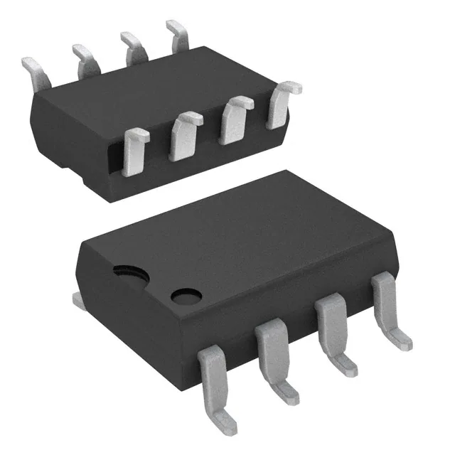
HCPL-3100, HCPL-3101
Power MOSFET/IGBT Gate Drive Optocouplers
Data Sheet
Description
Features
The HCPL-3100/3101 consists of an LED* optically
coupled to an integrated circuit with a power output
stage. These optocouplers are suited for driving
power MOSFETs and IGBTs used in motor control
inverter applications. The high operating voltage range
of the output stage provides the voltage drives required
by gate controlled devices. The voltage and current
supplied by these optocouplers allow for direct
interfacing to the power device without the need for an
intermediate amplifier stage.
• High output current IO1 and IO2
(0.6 A Peak, 0.1 A continuous)
• 15 kV/µs minimum Common Mode Rejection (CMR) at
VCM = 1500 V
• Wide operating VCC range (15 to 30 volts)
• High speed
– 1 µs typical propagation delay (HCPL-3100)
– 0.3 µs typical propagation delay (HCPL-3101)
• Recognized under UL 1577 for dielectric withstand proof
test voltages of 5000 vac, 1 minute
The HCPL-3100 switches a 3000 pF load in 2 µs and
the HCPL-3101, using a higher speed LED, switches a
3000 pF load in 0.5 µs. With a CMR rating of 15 kV/µs
typical these opto-couplers readily reject transients
found in inverter applications.
The LED controls the state of the output stage.
Transistor Q2 in the output stage is on with the LED off,
allowing the gate of the power device to be held low.
Turning on the LED turns off transistor Q2 and
switches on transistor Q1 in the output stage which
provides current and voltage to drive the gate of the
power device.
Applications
•
•
•
•
Isolated MOSFET/IGBT gate drive
AC and DC motor drives
General purpose industrial inverters
Uninterruptable power supply
Functional Diagram
HCPL-3100
ANODE
1
CATHODE
2
HCPL-3101
8
VCC
7
GND
1
ANODE
2
Q2
3
VCC
7
GND
6
V O2
5
V O1
Q2
6
VO2
CATHODE
3
Q1
4
8
Q1
5
VO1
TRUTH TABLE
LED
OUTPUT
ON
HIGH LEVEL
OFF
LOW LEVEL
4
Q1
ON
OFF
Q2
OFF
ON
THE USE OF A 0.1 µF BYPASS CAPACITOR CONNECTED BETWEEN PINS 8 AND 7
IS RECOMMENDED. ALSO CURRENT LIMITING RESISTOR IS RECOMMENDED
(SEE FIGURE 1, AND NOTE 2 AND NOTE 7).
*HCPL-3100 LED contains Silicon-doped GaAs and HCPL-3101
LED contains AlGaAs.
CAUTION: It is advised that normal static precautions be taken in handling and assembly of this component to
prevent damage and/or degradation which may be induced by ESD.
�Schematic
HCPL-3101
HCPL-3100
I CC
I CC
V CC
GND
GND
1
ANODE
2
ANODE
+
CATHODE
7
Q2
IF
6
Q1
–
5
IO2
V O2
CATHODE
IO1
2
V O1
7
Q2
IF
+
IO2
V CC
8
8
6
Q1
–
IO1
3
5
V O2
V O1
THE USE OF A 0.1 µF BYPASS CAPACITOR CONNECTED BETWEEN PINS 8 AND 7
IS RECOMMENDED. ALSO CURRENT LIMITING RESISTOR IS RECOMMENDED
(SEE FIGURE 1, AND NOTE 2 AND NOTE 7).
Ordering Information
HCPL-3100 and HCPL-3101 are UL Recognized with 5000 Vrms for 1 minute per UL1577.
Option
Part
Number
HCPL-3100
HCPL-3101
RoHS Compliant
-000E
-300E
-500E
Package
300 mil DIP-8
Surface
Mount
Gull
Wing
Tape
& Reel
X
X
X
X
X
Quantity
50 per tube
50 per tube
1000 per reel
To order, choose a part number from the part number column and combine with the desired option from the option
column to form an order entry.
Example 1:
HCPL-3100-500E to order product of 300 mil DIP Gull Wing Surface Mount package in Tape and Reel packaging and
RoHS compliant.
Example 2:
HCPL-3101-000E to order product of 300 mil DIP package in Tube packaging and RoHS compliant.
Option datasheets are available. Contact your Avago sales representative or authorized distributor for information.
Remarks: The notation ‘#XXX’ is used for existing products, while (new) products launched since July 15, 2001 and
RoHS compliant will use ‘–XXXE.’
2
�Outline Drawing
0.65 (0.026)
1.05 (0.040)
8
0.90 (0.035)
1.50 (0.059)
7
6
0°
13°
5
TYPE
NUMBER
0.16 (0.006)
0.36 (0.014)
A XXXX
DATE
CODE
6.00 (0.236)
7.00 (0.276)
YYWW
7.32 (0.288)
7.92 (0.312)
0°
13°
1
2
3
4
HCPL-3100
ANODE
1
CATHODE
2
HCPL-3101
8
VCC
7
GND
1
8
VCC
7
GND
6
V O2
5
V O1
9.16 (0.361)
10.16 (0.400)
0.50
(0.020)
TYP.
3.00 (0.118)
4.00 (0.157)
ANODE
2
Q2
3
Q2
6
VO2
CATHODE
3
Q1
2.90 (0.114)
3.90 (0.154)
2.55 (0.100)
3.55 (0.140)
0.40 (0.016)
0.60 (0.024)
2.29 (0.090)
2.79 (0.110)
3
4
Q1
5
VO1
4
�Demonstrated ESD
Performance
Regulatory Information
The HCPL-3100/3101 has been
approved by the following
organization:
Human Body Model: MIL-STD883 Method 3015.7: Class 2
Machine Model: EIAJ IC-1211988 (1988.3.28 Version 2),
Test Method 20, Condition
C: 1200 V
UL
Recognized under UL 1577,
Component Recognition
Program, File E55361.
Insulation and Safety Related Specifications
Parameter
Symbol
Value
Units
Conditions
Min. External Air Gap
(External Clearance)
L(IO1)
6.0
mm
Shortest distance measured through air, between two
conductive leads, input to output
Min. External Tracking
Path (External
Creepage)
L(IO2)
6.0
mm
Shortest distance path measured along outside surface
of optocoupler body between input and output leads
0.15
mm
Through insulation distance conductor to conductor
inside the optocoupler cavity
Min. Internal Plastic
Gap (Internal
Clearance)
Absolute Maximum Ratings
Parameter
Symbol
Device
Min.
Max.
Unit
-55
125
°C
-40
-40
100
85
°C
Conditions
Fig.
Note
Storage Temperature
TS
Operating Temperature
TA
HCPL-3100
HCPL-3101
Input
Continuous
Current
IF
HCPL-3100
25
mA
11
1
HCPL-3101
20
mA
11
1
Reverse
Voltage
VR
HCPL-3100
HCPL-3101
6
5
V
Supply Voltage VCC
Output 1
Continuous
Current
35
IO1
Peak Current
Output 2
V
0.1
A
0.6
A
Voltage
VO1
35
V
Continuous
Current
IO2
0.1
A
0.6
A
Peak Current
TA = 25°C
1
Pulse Width < 0.15 µs,
Duty cycle = 1%
1
1
Pulse Width < 0.15 µs,
Duty cycle = 1%
1
Output Power Dissipation
PO
500
mW
12
1
Total Power Dissipation
PT
550
mW
12
1
Lead Solder Temperature
4
270°C for 10 s, 1.0 mm below seating plane
�Recommended Operating Conditions
Parameter
Symbol
Power Supply Voltage
Device
Min.
Max.
Units
15
30
V
HCPL-3100
14
20
mA
HCPL-3101
15
20
mA
-40
70
°C
VCC
Input Current (ON)
IF
Operating Temperature
TA
Recommended Protection for
Output Transistors
During switching transitions, the
output transistors Q1 and Q2 of
the HCPL-3100/3101 can
conduct large amounts of
current. Figure 1 describes a
recommended circuit design
showing a current limiting
resistor R2 which is necessary in
order to prevent damage to the
output transistors Q1 and Q2.
(See Note 7.) A bypass capacitor
C1 is also recommended to
reduce power supply noise.
HCPL-3100/1
+5 V
8
C1
R3
7
ANODE
12 V
Q2
+ HVDC
CONTROL
INPUT
6
TTL
OR
LSTTL
IGBT
(OR )t
(MOSFET)
R2
CATHODE
Q1
5
TOTEM
POLE
OUTPUT
GATE
12 V
3-PHASE
AC
- HVDC
R2 = 25 - 100 Ω
R3 = 180 Ω (HCPL-3100)
240 Ω (HCPL-3101)
BYPASS CAPACITOR C1 = 0.1 µF
Figure 1. Recommended output transistor protection and typical application circuit.
5
�Electrical Specifications
Over recommended temperature (TA = -40°C to +100°C, HCPL-3100; TA = -40°C to +85°C, HCPL-3101) unless otherwise specified.
Parameter
Input Forward
Voltage
Sym.
Device
Min.
Typ.
Max.
Units
VF
HCPL-3100
-
1.2
1.4
V
IF = 20 mA
0.6
0.9
-
V
IF = 0.2 mA
-
1.6
1.75
V
IF = 10 mA
1.2
1.5
-
V
IF = 0.2 mA
-
-
10
µA
VR = 4 V
HCPL-3101
Input Reverse
Current
IR
HCPL-3100
HCPL-3101
Input Capacitance
Output 1
Output 2
CIN
Low
Level
Voltage
VO1L
Leakage
Current
IO1L
High
Level
Voltage
VO2H
Low
Level
Voltage
VO2L
Leakage
Current
IO2L
High
Level
30
250
pF
VF = 0 V, f = 1 kHz, TA = 25°C
HCPL-3101
-
60
150
pF
VF = 0 V, f = 1 MHz, TA = 25°C
HCPL-3100
-
0.2
0.4
V
IF = 10 mA
IF = 5 mA
Low
Level
Low to High
Threshold Input
-
500
µA
VCC = VO1 = 35 V, VO2 = 0 V
IF = 0 mA, TA = 25°C
20
22
-
V
IF = 10 mA
IF = 5 mA
4, 21,
22
0.8
V
VCC = VO1 = 24 V, IO2 = 0.1 A,
IF = 0 mA
-
-
500
µA
IF = 10 mA
VCC = 35 V,
VO2 = 35 V,
TA = 25°C
1.3
3.0
mA
VO1 = 24 V
VCC = 24 V, IF = 10 mA
HCPL-3101
-
1.3
3.0
mA
VO1 = 24 V
VCC = 24 V, IF = 5 mA
-
1.3
3.0
mA
VO1 = 24 V
VCC = 24 V, IF = 0 mA
7, 24
1.0
4.0
7.0
mA
TA = 25°C
8, 15,
16
0.6
-
10.0
mA
VCC = VO1 = 24 V
0.3
1.5
3.0
mA
TA = 25°C
0.2
-
5.0
mA
VCC = VO1 = 24 V
HCPL-3100
2
6
-
HCPL-3101
6
3, 19,
20
0.5
2
5
VCC = 24 V,
VO1 = 24 V,
IO2 = -0.1 A
-
IF = 5 mA
2, 17,
18
HCPL-3100
ICCL
IFLH
VCC1 = 12 V,
IO1 = 0.1 A,
VCC2 = -12 V
-
HCPL-3101
HCPL-3100
13
TA = 25°C
-
HCPL-3100
Note
14
HCPL-3100
HCPL-3101
ICCH
TA = 25°C
Fig.
VF = 5 V
HCPL-3101
Supply
Current
Test Conditions
7, 23
2
2, 3
�Switching Specifications (TA = 25°C)
Parameter
Sym.
Propagation
Delay Time to
High Output
Level
tPLH
Propagation
Delay Time to
Low Output
Level
tPHL
Rise Time
tr
Device
Min.
Typ.
Max.
Units
HCPL-3100
-
1
2
µs
IF = 10 mA
HCPL-3101
-
0.3
0.5
µs
IF = 5 mA
HCPL-3100
-
1
2
µs
IF = 10 mA
HCPL-3101
-
0.3
0.5
µs
IF = 5 mA
HCPL-3100
-
0.2
0.5
µs
IF = 10 mA
HCPL-3101
Fall Time
tf
|CMH|
HCPL-3100
Output Low
Level Common
Mode Transient
Immunity
|CML|
HCPL-3100
Fig.
Note
VCC = 24 V,
VO1 = 24 V,
RG = 47 Ω,
CG = 3000 pF
9,
25,
26,
27
2, 6
VCM = 1500 V
(peak),
VCC = 24 V
VO1 = 24 V
∆V02H = ∆V02L
= 2.0 V
10
2
IF = 5 mA
-
0.2
0.5
µs
HCPL-3101
Output High
Level Common
Mode Transient
Immunity
Test Conditions
IF = 10 mA
IF = 5 mA
15
-
kV/µs
IF = 10 mA
IF = 5mA
HCPL-3101
15
-
kV/µs
IF = 0 mA
Packaging Characteristics
Sym.
Min.
Input-Output Momentary
Withstand Voltage*
Parameter
VISO
5000
Typ.
Max.
Units
Resistance (Input-Output)
RI-O
5x10¹⁰
1011
–
Ω
VI-O = 500 V, TA = 25°C
RH = 40% to 60%
4
Capacitance (Input-Output)
CI-O
–
1.2
–
pF
f = 1 MHz
4
V rms
Test Conditions
RH = 40% to 60%
t = 1 min, TA = 25°C
Fig.
Note
4, 5
*The Input-Output Momentary Withstand Voltage is a dielectric voltage rating that should not be interpreted as an input-output continuous voltage
rating. For the continuous voltage rating refer to the IEC/EN/DIN EN 60747-5-2 Insulation Characteristics Table (if applicable), your equipment level
safety specification, or Avago Application Note 1074, “Optocoupler Input-Output Endurance Voltage.”
Notes:
1. Derate absolute maximum ratings with ambient temperatures as shown in Figures 11 and 12.
2. A bypass capacitor of 0.01 µF or more is needed near the device between VCC and GND when measuring output and transfer
characteristics.
3. IFLH represents the forward current when the output goes from low to high.
4. Device considered a two terminal device; pins 1-4 are shorted together and pins 5-8 are shorted together.
5. For devices with minimum VISO specified at 5000 V rms, in accordance with UL 1577, each optocoupler is proof-tested by
applying an insulation test voltage ≥ 6000 V rms for one second (leakage current detection limit, II-O ≤ 200 µA).
6. The tPLH and tPHL propagation delays are measured from the 50% level of the input pulse to the 50% level of the output pulse.
7. R2 limits the Q1 and Q2 peak currents. For more applications and circuit design information see Application Note “Power
Transistor Gate/Base Drive Optocouplers.”
7
�HCPL-3100
HCPL-3100
VCC
1
IF
GND
2
3
VCC1
7
VCC2
Q2
Q1
+
GND
2
IO1
+
5
3
Q1
VO1L
4
5
HCPL-3100
VCC
+
-
VCC
GND
7
Q2
3
6
Q1
4
VCC
1
8
IF
+
GND
2
–
VO2L
+
3
6
VO2
Q1
4
HCPL-3100
VCC
1
8
GND
VCC
7
4
3
V O2
4
5
8
VCC
7
3
6
Q1
4
+
-
–
V O2
+
V O2
5
V O1
Figure 8. Test circuit for threshold input current IFLH.
8
5
Figure 7. Test circuit for ICCH and ICCL.
HCPL-3100
Q2
V O2
V O1
Figure 6. Test circuit for leakage current IO2L.
GND
7
6
Q1
V O1
VCC
GND
Q2
IO2L
6
Q1
ICC
8
+
-
2
Q2
3
VCC
IF
+
-
IF
2
IO1L
5
Figure 5. Test circuit for leakage current IO1L.
HCPL-3100
1
VO2
V O1
Figure 4. Test circuit for low level output voltage VO2L.
SWEEP
V CC
7
Q2
IO2
VO1
IF
8
IF
5
2
+
VO2
Figure 3. Test circuit for high level output voltage VO2H.
HCPL-3100
1
IO2
VO1
Figure 2. Test circuit for low level output voltage VO1L.
2
–
VO2H
6
V O1
1
7
Q2
–
V O2
VCC
8
IF
+
-
+
-
6
4
VCC
1
8
V CC
�HCPL-3100
HCPL-3100
IF
VCC
1
t r = t f = 0.01 µs
V IN PULSE WIDTH 5 µs
DUTY RATIO 50%
IF
8
V CC
GND
2
7
3
6
Q1
4
+
-
–
V O2
+
Q2
VCC
1
V CC
GND
2
SW
7
A
V O2
B
3
+
6
VO2
Q1
5
+
-
–
Q2
CG
RG
V O2
8
4
5
VO1
VO1
–
+
V CM
V CM
50%
V IN WAVE FORM
V CM
t PLH
t PLH
GND
90%
CMH , VO2
50%
VOUT WAVE FORM
10%
tr
V O2H
SW AT A, IF = 10 mA, HCPL-3100
SW AT A, IF = 5 mA, HCPL-3101
∆ VO2H
tf
∆ VO2L
CM L , VO2
V O2L
GND
SW AT B, I F = 0 mA
60
50
50
40
30
20
10
0
25
50
75
100
125
AMBIENT TEMPERATURE TA (°C)
Figure 11. LED forward current vs. ambient
temperature, HCPL-3100.
600
POWER DISSIPATION PO, Ptot (mW)
60
0
-40 -25
9
Figure 10. Test circuit for CMH and CML.
FORWARD CURRENT IF (mA)
FORWARD CURRENT IF (mA)
Figure 9. Test circuit for tPLH, tPHL, tr, and tf.
40
30
20
10
0
-40 -25
0
25
50
75 85 100
125
AMBIENT TEMPERATURE TA (°C)
Figure 12. LED forward current vs. ambient
temperature, HCPL-3101.
500
Ptot
PO
400
300
200
100
0
-40 -25
0
25
50
75
100
AMBIENT TEMPERATURE TA (°C)
Figure 13. Maximum power dissipation
vs. ambient temperature, HCPL-3100.
125
�100
Ptot
PO
400
300
200
100
100
FORWARD CURRENT IF (mA)
500
FORWARD CURRENT IF (mA)
POWER DISSIPATION PO, Ptot (mW)
600
25°C
10
TA = 100°C
0°C
85°C
1
-40°C
0°C
10
TA = 85°C
-20°C
50°C
-40°C
1
50°C
25°C
25
50
75 85 100
0.1
0.50
125
0.75
120
TA = 25°C
110
VALUE OF VCC = 24 V
ASSUME 100
100
90
80
21
24
27
30
VCC = 24 V
110
100
IFLH = 100% at TA = 25°C
80
70
0
20
40
60
80
100
AMBIENT TEMPERATURE TA (°C)
Figure 20. Normalized low to high threshold
input current vs. ambient temperature,
HCPL-3101.
10
1.2
TA = 25°C
110
100
90
IFLH = 100% at VCC = 24 V
80
70
15
18
21
24
27
2
1
0.2
0.3
0.4
2.0
2.2
160
VCC = 24 V
140
120
IFLH = 100% at TA = 25°C
100
80
60
-40
-20
0
40
20
60
80
100
Figure 19. Normalized low to high threshold
input current vs. ambient temperature,
HCPL-3100.
3
TA = 25°C
VCC1 = 12 V
VCC2 = -12 V
IF = 5 mA
2
1
0
0.1
1.8
AMBIENT TEMPERATURE TA (°C)
TA = 25°C
VCC1 = 12 V
VCC2 = -12 V
IF = 10 mA
0
1.6
Figure 16. Typical forward current vs. forward
voltage, HCPL-3101.
30
3
0
1.4
FORWARD VOLTAGE VF (V)
Figure 18. Normalized low to high threshold
input current vs. supply voltage, HCPL-3101.
O1 LOW LEVEL OUTPUT VOLTAGE VO1L (V)
RELATIVE INPUT THRESHOLD CURRENT (%)
120
-20
0.1
1.0
2.00
SUPPLY VOLTAGE VCC (V)
Figure 17. Normalized low to high threshold
input current vs. supply voltage, HCPL-3100.
60
-40
1.75
120
SUPPLY VOLTAGE VCC (V)
90
1.50
Figure 15. Typical forward current vs. forward
voltage, HCPL-3100.
RELATIVE INPUT THRESHOLD CURRENT (%)
RELATIVE INPUT THRESHOLD CURRENT (%)
Figure 14. Maximum power dissipation
vs. ambient temperature, HCPL-3101.
18
1.25
FORWARD VOLTAGE VF (V)
AMBIENT TEMPERATURE TA (°C)
70
15
1.00
RELATIVE INPUT THRESHOLD CURRENT (%)
0
O1 LOW LEVEL OUTPUT VOLTAGE VO1L (V)
0
-40 -25
0.5
0.6
O1 OUTPUT CURRENT IO1 (A)
Figure 21. Typical low level output 1 voltage
vs. output 1 current, HCPL-3100.
0
0.1
0.2
0.3
0.4
0.5
0.6
O1 OUTPUT CURRENT IO1 (A)
Figure 22. Typical low level output 1 voltage
vs. output 1 current, HCPL-3101.
�VCC1 = 12 V
VCC2 = -12 V
IF = 10 mA
IO2 = 0.1 A
0.20
0.15
0.10
0.05
-20
0
20
40
60
80
0.25
0.20
0.15
0.10
0.05
0
-40
100
30
TA = 25°C
IF = 5 mA
24
21
18
15
21
18
24
27
30
TA = 25°C
VCC = VO1 = 24 V
IF = 0 mA
2
1
0.2
0.3
0.4
0.5
0.6
O2 OUTPUT CURRENT IO2 (A)
Figure 29. Typical low level output 2 voltage
vs. output 2 current, HCPL-3100.
11
80
100
TA = 25°C
IF = 10 mA
24
21
18
15
12
15
IO2 NEARLY = 0 A
23
IO2 = -0.1 A
22
21
VCC = 24 V
IF = 10 mA
20
-40
-20
0
20
40
60
80
2
1
0.1
0.2
0.3
0.4
0.5
27
30
24
IO2 = NEARLY 0 A
23
IO2 = -0.1 A
22
21
VCC = 24 V
IF = 5 mA
20
-40
-20
0
20
40
60
80
100
AMBIENT TEMPERATURE TA (°C)
TA = 25°C
VCC = VO1 = 24 V
IF = 0 mA
0
24
Figure 25. Typical high level output 2 voltage
vs. supply voltage, HCPL-3100.
100
3
0
21
18
SUPPLY VOLTAGE VCC (V)
Figure 27. Typical high level output 2 voltage
vs. ambient temperature, HCPL-3100.
O2 LOW LEVEL OUTPUT VOLTAGE VO2L (V)
O2 LOW LEVEL OUTPUT VOLTAGE VO2L (V)
3
0.1
60
27
AMBIENT TEMPERATURE TA (°C)
Figure 26. Typical high level output 2 voltage
vs. supply voltage, HCPL-3101.
0
40
24
SUPPLY VOLTAGE VCC (V)
0
20
Figure 24. Typical low level output 1 voltage
vs. ambient temperature, HCPL-3101.
O2 HIGH LEVEL OUTPUT VOLTAGE VO2H (V)
O2 HIGH LEVEL OUTPUT VOLTAGE VO2H (V)
Figure 23. Typical low level output 1 voltage
vs. ambient temperature, HCPL-3100.
12
15
0
30
AMBIENT TEMPERATURE TA (°C)
AMBIENT TEMPERATURE TA (°C)
27
-20
O2 HIGH LEVEL OUTPUT VOLTAGE VO2H (V)
0
-40
VCC1 = 12 V
VCC2 = -12 V
IF = 5 mA
IO2 = 0.1 A
Figure 28. Typical high level output 2 voltage
vs. ambient temperature, HCPL-3101.
O2 LOW LEVEL OUTPUT VOLTAGE VO2L (V)
0.25
0.30
O2 HIGH LEVEL OUTPUT VOLTAGE VO2H (V)
O1 LOW LEVEL OUTPUT VOLTAGE VO1L (V)
O1 LOW LEVEL OUTPUT VOLTAGE VO1L (V)
0.30
0.6
O2 OUTPUT CURRENT IO2 (A)
Figure 30. Typical low level output 2 voltage
vs. output 2 current, HCPL-3101.
0.8
VCC = 24 V
IF = 0 mA
IO2 = 0.1 A
0.7
0.6
0.5
0.4
0.3
0.2
-40
-20
0
20
40
60
80
100
AMBIENT TEMPERATURE TA (°C)
Figure 31. Typical low level output 2 voltage
vs. ambient temperature, HCPL-3100.
�VCC = 24 V
IF = 0 mA
IO2 = 0.1 A
0.7
0.6
0.5
0.4
0.3
-20
0
20
40
60
80
2.5
2.0
1.5
1.0
0.5
0
15
100
TA = 25°C
IF = 10 mA
Figure 32. Typical low level output 2 voltage
vs. ambient temperature, HCPL-3101.
2.0
1.5
1.0
0.5
21
18
24
27
TA = 25°C
IF = 0 mA
2.5
2.0
1.5
1.0
0.5
0
15
30
VCC = 24 V
IF = 5 mA
2.0
1.5
1.0
0.5
0
20
40
60
0.5
24
80
100
27
AMBIENT TEMPERATURE TA (°C)
Figure 38. Typical high level supply current
vs. ambient temperature, HCPL-3101.
24
27
30
3.0
VCC = 24 V
IF = 10 mA
2.5
2.0
1.5
1.0
0.5
0
-40
30
-20
0
20
40
60
80
100
AMBIENT TEMPERATURE TA (°C)
Figure 37. Typical high level supply current
vs. ambient temperature, HCPL-3100.
3.0
VCC = 24 V
IF = 0 mA
2.5
2.0
1.5
1.0
0.5
0
-40
21
18
Figure 34. Typical high level supply current
vs. supply voltage, HCPL-3101.
3.0
LOW LEVEL SUPPLY CURRENT ICCL (mA)
HIGH LEVEL SUPPLY CURRENT ICCH (mA)
21
18
Figure 36. Typical low level supply current
vs. supply voltage, HCPL-3101.
3.0
-20
1.0
SUPPLY VOLTAGE VCC (V)
Figure 35. Typical low level supply current
vs. supply voltage, HCPL-3100.
2.5
1.5
SUPPLY VOLTAGE VCC (V)
HIGH LEVEL SUPPLY CURRENT ICCH (mA)
LOW LEVEL SUPPLY CURRENT ICCL (mA)
LOW LEVEL SUPPLY CURRENT ICCL (mA)
TA = 25°C
IF = 0 mA
2.5
2.0
0
15
30
3.0
SUPPLY VOLTAGE VCC (V)
12
27
Figure 33. Typical high level supply current
vs. supply voltage, HCPL-3100.
3.0
0
-40
24
TA = 25°C
IF = 5 mA
2.5
SUPPLY VOLTAGE VCC (V)
AMBIENT TEMPERATURE TA (°C)
0
15
21
18
LOW LEVEL SUPPLY CURRENT ICCL (mA)
0.2
-40
3.0
HIGH LEVEL SUPPLY CURRENT ICCH (mA)
HIGH LEVEL SUPPLY CURRENT ICCH (mA)
O2 LOW LEVEL OUTPUT VOLTAGE VO2L (V)
3.0
0.8
-20
0
20
40
60
80
AMBIENT TEMPERATURE TA (°C)
Figure 39. Typical low level supply current
vs. ambient temperature, HCPL-3100.
100
VCC = 24 V
IF = 0 mA
2.5
2.0
1.5
1.0
0.5
0
-40
-20
0
20
40
60
80
100
AMBIENT TEMPERATURE TA (°C)
Figure 40. Typical low level supply current
vs. ambient temperature, HCPL-3101.
�VCC = VO1 = 24 V
RG = 47 W
CG = 3000 pF
2.0
1.5
TA = 85°C
25°C
-40°C
1.0
0.5
0
-40°C
0
5
25°C
10
85°C
15
20
25
FORWARD CURRENT IF (mA)
PROPAGATION DELAY TIME tPHL, tPLH (µs)
VCC = VO1 = 24 V
RG = 47 W
CG = 3000 pF
IF = 5 mA
0.6
tPLH
tPHL
0.2
0
-40
-20
0
20
40
60
80
AMBIENT TEMPERATURE TA (°C)
Figure 44. Typical propagation delay time
vs. ambient temperature, HCPL-3101.
13
VCC = VO1 = 24 V
RG = 47 W
CG = 3000 pF
0.8
0.6
TA = 85°C
25°C
-40°C
0.4
0.2
0
85°C
0
5
25°C
10
-40°C
15
20
Figure 42. Typical propagation delay time
vs. forward current, HCPL-3101.
1.0
0.4
tPHL
tPLH
FORWARD CURRENT IF (mA)
Figure 41. Typical propagation delay time
vs. forward current, HCPL-3100.
0.8
1.0
100
PROPAGATION DELAY TIME tPHL, tPLH (µs)
tPHL
tPLH
PROPAGATION DELAY TIME tPHL, tPLH (µs)
PROPAGATION DELAY TIME tPHL, tPLH (µs)
2.5
25
2.5
VCC = VO1 = 24 V
RG = 47 W
CG = 3000 pF
IF = 10 mA
2.0
1.5
1.0
tPHL
0.5
0
-40
tPLH
-20
0
20
40
60
80
AMBIENT TEMPERATURE TA (°C)
Figure 43. Typical propagation delay time
vs. ambient temperature, HCPL-3100.
100
�For product information and a complete list of distributors, please go to our website:
www.avagotech.com
Avago, Avago Technologies, and the A logo are trademarks of Avago Technologies Limited in the United States and other countries.
Data subject to change. Copyright © 2007 Avago Technologies Limited. All rights reserved. Obsoletes 5989-2939EN
AV01-0573EN July 16, 2007
�