Data Sheet
4N55, 5962-87679, HCPL-553x, HCPL-653x,
HCPL-257K, HCPL-655x, 5962-90854,
HCPL-550x
Hermetically Sealed, Transistor Output
Optocouplers for Analog and Digital
Applications
Description
Features
These units are single-, dual-, and quad-channel,
hermetically sealed optocouplers. The products are capable
of operation and storage over the full military temperature
range and can be purchased as either Commercial product
or with full MIL-PRF-38534 Class Level H or K testing or
from the appropriate DLA Standard Microcircuit Drawing
(SMD). All devices are manufactured and tested on a MILPRF-38534 certified line and Class H and K devices are
included in the DLA Qualified Manufacturers List QML38534 for Hybrid Microcircuits.
CAUTION! It is advised that normal static precautions be
taken in handling and assembly of this
component to prevent damage and/or
degradation which may be induced by ESD.
Dual marked with device part number and DLA
Standard Microcircuit Drawing (SMD)
Manufactured and tested on a MIL-PRF-38534 Certified
Line
QML-38534, Class H and K
Five hermetically sealed package configurations
Performance guaranteed over full military temperature
range: –55°C to +125°C
High speed: 400 kb/s typical
9-MHz bandwidth
Open collector output
VCC ranges from 2V to 18V
1500 VDC withstand test voltage
High radiation immunity
6N135, 6N136, HCPL-2530/2531 function compatibility
Reliability data
Applications
1.
Broadcom
Military and aerospace
High reliability systems
Vehicle command, control, life critical systems
Line receiver
Switching power supply
Voltage level shifting
Analog signal ground isolation (see Figures 7, 8, and 13)
Isolated input line receiver
Isolated output line driver
Logic ground isolation
Harsh industrial environments
Isolation for test equipment systems
See the Selection Guide – Package Styles and Lead Configuration Options table for available extensions.
AV02-3846EN
June 27, 2019
�4N55, 5962-87679, HCPL-553x, HCPL-653x, HCPL-257K, HCPL-655x, 596290854, HCPL-550x Data Sheet
Functional Diagram
V CC
VB
VO
GND
Multiple channel devices are available.
Truth Table
(Positive Logic)
Input
Output
On (H)
L
Off (L)
H
NOTE:
Broadcom
The connection of a 0.1 µF bypass capacitor
between VCC and GND is recommended.
Hermetically Sealed, Transistor Output Optocouplers for Analog and Digital Applications
Each channel contains a GaAsP light emitting diode that is
optically coupled to an integrated photon detector. Separate
connections for the photodiodes and output transistor
collectors improve the speed up to one-hundred times that
of a conventional phototransistor optocoupler by reducing
the base-collector capacitance.
These devices are suitable for wide-bandwidth analog
applications, as well as for interfacing TTL to LSTTL or
CMOS. Current Transfer Ratio (CTR) is 9% minimum at IF =
16 mA. The 18V VCC capability enables the designer to
interface any TTL family to CMOS. The availability of the
base lead allows optimized gain/bandwidth adjustment in
analog applications. The shallow depth of the IC photodiode
provides better radiation immunity than conventional
phototransistor couplers.
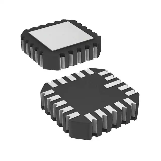
Package styles for these parts are 8- and 16-pin DIP
through-hole (case outlines P and E, respectively), 16-pin
DIP flat pack (case outline F), and leadless ceramic chip
carrier (case outline 2). Devices may be purchased with a
variety of lead bend and plating options, see the selection
guide table for details. Standard Microcircuit Drawing (SMD)
parts are available for each package and lead style.
Because the same functional die (emitters and detectors)
are used for each channel of each device listed in this data
sheet, absolute maximum ratings, recommended operating
conditions, electrical specifications, and performance
characteristics shown in the figures are identical for all parts.
Occasional exceptions exist due to package variations and
limitations and are as noted. Additionally, the same package
assembly processes and materials are used in all devices.
These similarities give justification for the use of data
obtained from one part to represent other part’s
performance for die related reliability and certain limited
radiation test results.
AV02-3846EN
2
�4N55, 5962-87679, HCPL-553x, HCPL-653x, HCPL-257K, HCPL-655x, 596290854, HCPL-550x Data Sheet
Hermetically Sealed, Transistor Output Optocouplers for Analog and Digital Applications
Selection Guide – Package Styles and Lead Configuration Options
Package
16-Pin DIP
8-Pin DIP
8-Pin DIP
16-Pin Flat Pack
20-Pad LCCC
Lead Style
Through Hole
Through Hole
Through Hole
Unformed Leads
Surface Mount
Channels
2
1
2
4
2
Common Channel Wiring
None
None
VCC, GND
VCC, GND
None
Commercial
4N55
HCPL-5500
HCPL-5530
HCPL-6550
HCPL-6530
MIL-PRF-38534, Class H
4N55/883B
HCPL-5501
HCPL-5531
HCPL-6551
HCPL-6531
MIL-PRF-38534, Class K
HCPL-257K
HCPL-550K
HCPL-553K
HCPL-655K
HCPL-653K
a
a
a
a
Part Number and Options
Standard Lead Finish
Gold Plate
Solder Dippedb
Option #200
Option #200
Option #200
Option #100
Option #100
Option #100
Option #300
Option #300
Option #300
Prescript for all below
5962-
5962-
5962-
5962-
Gold Platea
8767901EC
9085401HPC
8767902PC
8767904FC
Solder Dippedb
8767901EA
9085401HPA
8767902PA
Butt Joint/Gold Platea
8767901UC
9085401HYC
8767902YC
Butt Joint/Solderedb
8767901UA
9085401HYA
8767902YA
Gull Wing/Solderedb
8767901TA
9085401HXA
8767902XA
Butt Joint/Gold
Gull
Platea
Wing/Solderedb
Gold Plate
Gold Plate
Gold Plate
Solder Padsb
Class H SMD Part Number
596287679032A
Class K SMD Part Number
Prescript for all below
5962-
5962-
5962-
5962-
8767905KEC
9085401KPC
8767906KPC
8767908KFC
Solder Dippedb
8767905KEA
9085401KPA
8767906KPA
Butt Joint/Gold Platea
Gold
Butt
Platea
8767905KUC
9085401KYC
8767906KYC
Joint/Solderedb
8767905KUA
9085401KYA
8767906KYA
b
8767905KTA
9085401KXA
8767906KXA
Gull Wing/Soldered
59628767907K2A
a. Gold Plate lead finish: Maximum gold thickness of leads is 2.0V).
e. Bandwidth is the frequency at which the ac output voltage is 3 dB below the low frequency asymptote. For the HCPL-553x the typical
bandwidth is 2 MHz.
Multi-Channel Product Only
Parameter
Symbol
Test Conditions
Typ.
Units
Note
Input-Input Insulation Leakage Current
II-I
Relative Humidity ≤ 65%
VI-I = 500V, t = 5s
1
pA
a, b
Resistance (Input-Input)
RI-I
VI-I = 500V
1012
Ω
a
Capacitance (Input-Input)
CI-I
f = 1 MHz
0.8
pF
a
a. Measured between adjacent input pairs shorted together for each multichannel device.
b. This is a momentary withstand test, not an operating condition.
Broadcom
AV02-3846EN
10
�4N55, 5962-87679, HCPL-553x, HCPL-653x, HCPL-257K, HCPL-655x, 596290854, HCPL-550x Data Sheet
Figure 1: Input Diode Forward Current vs. Forward Voltage
Hermetically Sealed, Transistor Output Optocouplers for Analog and Digital Applications
Figure 2: DC and Pulsed Transfer Characteristic
20
100
1.0
16
IF
IO - Output Current (mA)
IF - Forward Current (mA)
10
VCC = 5V
TA = 25°C
18
TA = 25°C
+
VF
–
0.1
0.01
14
12
mA
IF = 40
mA
5
3
IF =
mA
IF = 30
mA
5
2
=
IF
mA
0
IF = 2
mA
5
1
=
IF
mA
0
1
=
F
I
A
m
5
IF =
10
8
6
4
2
0.001
1.10
1.20
1.30
1.40
1.50
0
1.60
0
2
4
6
VF - Forward Voltage (V)
Figure 3: Normalized Current Transfer Ratio vs. Input Diode
Forward Current
TA = +25°C
TA = –55°C
TA = +125°C
0.5
Normalized to:
CTR at IF = 16 mA, TA = 25°C
0.1
1
10
IOH - LOGIC HIGH OUTPUT CURRENT (μA)
CTR - Normalized Current Transfer Ratio
100
VCC = 5V
VO = 0.4V
0
10
14
16
18
20
1
I F = 0 μA,
IF (OTHER CHANNELS) = 20 mA
IF = I F (OTHER CHANNELS)
= 0 mA
0.1
VCC = VO = 18V
0.01
0.001
–60 –40 –20 0
100
20 40 60 80 100 120 140
TA - TEMPERATURE (°C)
Figure 5: Logic Low Supply Current vs. Input Diode Forward
Current
Figure 6: Propagation Delay vs. Temperature
50
4.0
TA = –55°C
45
3.6
40
tP - Propagation Delay (μs)
ICCL - Logic Low Supply Current (μA)
12
IF = 250 μA,
IF (OTHER CHANNELS) = 20 mA
IF - Input Diode Forward Current (mA)
TA = +25°C
35
30
TA = +125°C
25
20
15
3.2
2.0
1.6
1.2
5
0.4
5
10
15
20
IF - Input Diode Forward Current (mA)
Broadcom
25
tPLH
2.4
0.8
0
IF = 16 mA
VCC = 5V
RL = 8.2 kΩ
2.8
10
0
10
Figure 4: Logic High Output Current vs. Temperature
1.5
1.0
8
VO - Output Voltage (V)
0
–60 –40 –20
tPHL
0
20
40
60
80 100 120 140
TA - Temperature (°C)
AV02-3846EN
11
�4N55, 5962-87679, HCPL-553x, HCPL-653x, HCPL-257K, HCPL-655x, 596290854, HCPL-550x Data Sheet
Hermetically Sealed, Transistor Output Optocouplers for Analog and Digital Applications
Figure 8: Frequency Response
2.0
+15
TA = 25°C
VO = 2V
VCC = 5V
1.8
1.6
1.4
1.2
1.0
0.8
Normalized to:
IF = 16 mA
0.6
0.4
0.2
0
TA = 25°C
+10
NORMALIZED RESPONSE (dB)
ΔIO/ΔIF - Normalized Small Current Transfer Ratio
Figure 7: Normalized Small Signal Current Transfer Ratio vs.
Quiescent Input Current
INDEPENDENT
VCC DEVICES
+5
0
–5
–10
COMMON VCC
DEVICES
–15
–20
0.1
0
5
10
15
20
1.0
10
f - FREQUENCY (MHz)
25
100
IF - Quiescent Input Current (mA)
+12V
D.U.T.
+12V
0.1 μF
0.1 μF
1.2 kΩ
VCC
2.1 k Ω
47 μF
Q1
V IN
15 k Ω
100Ω
RF
1 kΩ
Q3
0.01 μF
Q2
VB
100 Ω
51Ω
9.1 k Ω
VO
470Ω
0.01 μF
VO
(1 M Ω, 12 pF
TEST INPUT)
GND
22 Ω
SINGLE CHANNEL TESTING,
INDEPENDENT VCC DEVICES
1N4150
TRIM FOR UNITY GAIN
Q 1, Q 2 , Q 3 : 2N3904
TYPICAL LINEARITY = +3% AT VIN = 1 VP-P
TYPICAL SNR = 50 dB
TYPICAL RF = 375Ω
TYPICAL VO dc = 3.8 V
TYPICAL IF = 9 mA
D.U.T.
+5V
+15V
VCC
20 kΩ
SET I F
VO
2N3053
1.6 Vdc
0.25 VP-P ac
AC INPUT
0.1 μF
560 Ω
100 Ω
100Ω
GND
COMMON
VCC DEVICES
Broadcom
AV02-3846EN
12
�4N55, 5962-87679, HCPL-553x, HCPL-653x, HCPL-257K, HCPL-655x, 596290854, HCPL-550x Data Sheet
Hermetically Sealed, Transistor Output Optocouplers for Analog and Digital Applications
Figure 9: Switching Test Circuit
IF
PULSE GEN.
Z O = 50 Ω
tr = 5 ns
0
D.U.T.
IF
+5V
VCC
RL
IF MONITOR
100Ω
5V
VO
VO
C L* = 50 pF
1.5V
GND
1.5V
VOL
SINGLE CHANNEL
OR COMMON VCC DEVICES
tPHL
tPLH
10% DUTY CYCLE
1/f < 100 μs
NOTES:
* C L INCLUDES PROBE AND STRAY WIRING CAPACITANCE.
BASE LEAD NOT CONNECTED.
Figure 10: Test Circuit for Transient Immunity and Typical
Waveforms
IF
VCM
B
D.U.T.
0V
+5V
VCC
RM
90%
10%
RL
A
90%
tr
VO
V FF
10%
tf
GND
VO
SINGLE CHANNEL OR
COMMON VCC DEVICES
5V
Switch at A: IF = 0 mA
V CM
+
PULSE GEN.
NOTE: BASE LEAD NOT CONNECTED.
VO
VOL
Switch at B: IF = 16 mA
Figure 11: Recommended Logic Interface
VCC
5V
Logic Family
220 Ω
RL
D.U.T.
Device #
VCC
VCC
RL 5% Tolerance
TTL
LOGIC GATE
0.01 μF
GND
LSTTL
CMOS
54LS14
CD40106BM
5V
a
18 kΩ
5V
15V
8.2 kΩ
22 kΩ
a. The equivalent output load resistance is affected by the
LSTTL input current and is approximately 8.2 kΩ. This is a
worst case design that takes into account 25% degradation
of CTR.
EACH CHANNEL
Broadcom
AV02-3846EN
13
�4N55, 5962-87679, HCPL-553x, HCPL-653x, HCPL-257K, HCPL-655x, 596290854, HCPL-550x Data Sheet
Hermetically Sealed, Transistor Output Optocouplers for Analog and Digital Applications
Figure 12: Operating Circuit for Burn-In and Steady State Life Tests (All Channels Tested Simultaneously)
V CC
V OC
D.U.T.*
V CC
(EACH INPUT)
+
0.1 μF
-
VO
V IN
GND
(EACH OUTPUT)
NOMINAL CONDITIONS
PER CHANNEL:
IF = 20 mA
IO = 4 mA
ICC = 30 μA
NOTE: BASE LEAD NOT CONNECTED.
T A = +125°C
Figure 13: Isolation Amplifier Application Circuit
IF 1
–
U1
+
+
VIN
1
8
2
7
3
6
4
5
220 Ω
IC
1
IC
2
U3
+
IF2
–
U2
+
–
R1
2.7 kΩ
R2
2.7 kΩ
2
R 4 1 kΩ
5 kΩ GAIN ADJUST
–15V
–
U4
+
U 1 , U 2 , U 3 , U 4 , LM307
IC = K1
1
1
IF
1
IF
2
R5
50 kΩ
VOUT
2
n1
IF
OFFSET ADJUST
5 kΩ
R3
2
HCPL-553x
I CC
6 mA
´
IC = K2
2
IF
n2
–15 V
´
2
Description
The schematic uses a dual-channel, high-speed optocoupler (HCPL-553x) to function as a servo type DC isolation amplifier.
This circuit operates on the principle that two optocouplers will track each other if their gain changes by the same amount
over a specific operating region.
Performance of Circuit
1% linearity for 10V peak-to-peak dynamic range
Gain drift: –0.03%/°C
Offset Drift: ±1 mV/°C
25 kHz bandwidth (limited by Op-Amps U1, U2)
Broadcom
AV02-3846EN
14
�Broadcom, the pulse logo, Connecting everything, Avago Technologies, Avago, and the A logo are among the trademarks
of Broadcom and/or its affiliates in the United States, certain other countries, and/or the EU.
Copyright © 2012–2019 Broadcom. All Rights Reserved.
The term “Broadcom” refers to Broadcom Inc. and/or its subsidiaries. For more information, please visit www.broadcom.com.
Broadcom reserves the right to make changes without further notice to any products or data herein to improve reliability,
function, or design. Information furnished by Broadcom is believed to be accurate and reliable. However, Broadcom does
not assume any liability arising out of the application or use of this information, nor the application or use of any product or
circuit described herein, neither does it convey any license under its patent rights nor the rights of others.
�


 工商网监
湘ICP备2023018690号
工商网监
湘ICP备2023018690号
