HFBR-1505AFZ/2505AFZ (SMA Tx/Rx for SERCOS)
HFBR-1515BFZ/2515BFZ (ST® Tx/Rx for PROFIBUS)
HFBR-1505CFZ/2505CFZ (SMA Tx/Rx for INTERBUS-S)
Full Metal Fiber Optic Transmitters and Receivers
for SERCOS, PROFIBUS and INTERBUS-S Applications
Data Sheet
Description
Features
SERCOS
• Meets industrial SERCOS, PROFIBUS, and INTERBUS-S
standard
SERCOS, an acronym for SErial Realtime COmmunications
System, is a standard digital interface for communication
in industrial CNC applications. SERCOS is a European (EN
61491) and international standard (IEC 61491). The optical
interface allows data rates of 2, 4, 8, and 16 MBd and data
transfer between numerical controls and drives via fiberoptic rings, with voltage isolation and noise immunity.
The HFBR-1505AFZ and HFBR-2505AFZ products comply
with SERCOS specifications for optical characteristics and
connector style, and have guaranteed performance up to
10 MBd. (16MBd SERCOS device is also available, please
contact Avago for more information.)
PROFIBUS
PROFIBUS, an acronym of PROcess FIeld BUS, is an open
fieldbus standard defined for data rates ranging from 9.6
kBd to 12 MBd in selectable steps for wire and optical
fiber. PROFIBUS is a German national DIN 19245 standard and a European CENELEC standard EN 50170. The
ST® connector is the recommended optical port of the
PROFIBUS optical fiber version but other connectors are
allowed as well. The HFBR-1515BFZ and HFBR-2515BFZ
comply fully to the technical guideline using Plastic
Optical Fiber up to 6 MBd, and have a guaranteed performance at data rates up to 10 MBd.
• SMA and ST® ports
• 650 nm wavelength technology
• Metal housing and port
• Specified for use with 1 mm plastic optical fiber and
200 µm hard clad silica
• Auto-insertable and wave solderable
• DC – 10 MBd data rate
• RoHS-compliant
Applications
• Industrial control data links
• Factory automation data links
• Voltage isolation applications
• PLCs
• Motor drives
• Sensor, meter and actuator interfaces
INTERBUS-S
INTERBUS-S, a special open Sensor/Actuator Bus, is
finding a broad acceptance in the factory automation
industry. The HFBR-1505CFZ and HFBR-2505CFZ were
specially designed for this application and can be used
with 1 mm POF and 200 µm HCS fiber at the specified
data rates of 500 kBd and 2 MBd. The optical transmission guideline is a supplement of the German National
DIN E 19258 standard draft. On the European level, prEN
50254 is the draft of the INTERBUS-S fieldbus.
ST® is a registered trademark of AT&T.
HCS® is a registered trademark of OFS Corporation.
Specifications and content subject to change without prior notification.
�Package Information
All HFBR-X5X5XFZ series transmitters and receivers are
housed in a dual-in-line metal package that is high
strength. The package is designed for auto-insertion and
wave soldering so it is ideal for high volume production
applications.
Handling and Design Information
When soldering, it is advisable to leave the protective
cap on the unit to keep the optics clean. Good system
performance requires clean port optics and cable ferrules
to avoid obstructing the optical path. Clean compressed
air often is sufficient to remove particles of dirt; methanol
on a cotton swab also works well.
Recommended Chemicals for Cleaning/Degreasing
HFBR-X5X5XFZ Products
Alcohols: methyl, isopropyl, isobutyl.
Aliphatics: hexane, heptane.
Other: soap solution, naphtha.
Do not use partially halogenated hydrocarbons such as
1,1,1 trichloroethane, ketones such as MEK, acetone,
chloroform, ethyl acetate, methylene dichloride, phenol,
methylene chloride or N-methylpyrolldone. Also, Avago
does not recommend the use of cleaners that use
halogenated hydrocarbons because of their potential
environmental harm.
CAUTION: The small junction size inherent in the design of these components increases the components’ susceptibility
to damage from electrostatic discharge (ESD). It is advised that normal static precautions be taken in handling and
assembly of these components to prevent damage and/or degradation which may be induced by ESD.
Specified Link Performance
-40˚C to +85°C unless otherwise noted.
Parameter
Symbol
Min.
Max.
Unit
Condition
Reference
Link Distance with
1
HFBR-1505AFZ/2505AFZ or
HFBR-1515BFZ/2515BFZ
0.1
0.1
40
100
m
m
POF
HCS®
Notes 1, 2, 3, 4, 6
Notes 1, 2, 3, 5, 6
Link Distance with
1
HFBR-1505CFZ/2505CFZ
0.1
0.1
50
300
m
m
POF
HCS®
Notes 1, 2, 3, 4, 7
Notes 1, 2, 3, 5, 7
Pulse Width Distortion
PWD
–30
+30
ns
with HFBR-1505AFZ/2505AFZ
or HFBR-1515BFZ/2515BFZ
25% to 75%
duty cycle
Note 1
Pulse Width Distortion
PWD
–125
+125
ns
with HFBR-1505CFZ/2505CFZ
arbitrary duty cycle
Note 1
Notes:
1. With recommended Tx and Rx circuits (60 mA nominal drive current).
2. POF HFBR-ExxyyyZ 0.23 dB/m worst case attentuation.
3. HCS Worst Case Attenuation is 10dB/km (0°C to 70°C) and 12dB/km (-40°C to 85°C).
4. Including a 3 dB optical safety margin accounting for link service lifetime.
5. Including a 2 dB optical safety margin accounting for link service lifetime.
6. Signaling rate DC to 10 MBd.
7. Signaling rate DC to 2 MBd.
�
Specifications and content subject to change without prior notification.
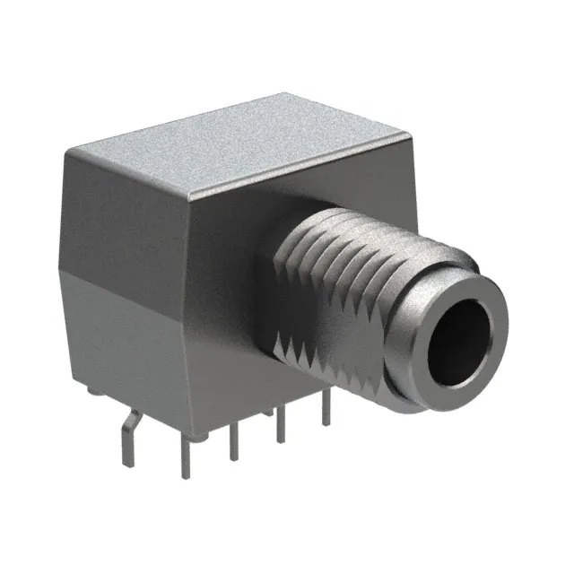
�HFBR-15X5XFZ Transmitters
4
5
6
The HFBR-15X5XFZ transmitter incorporates a 650 nm
LED in a metal housing. The high light output power
enables the use of both plastic optical fiber (POF) and
Hard Clad Silica (HCS®). This transmitter can be operated
up to 10 MBd using a simple driver circuit. The HFBR1505XFZ is compatible with SMA connectors, while the
HFBR-1515XFZ mates with ST® connectors.
7
1
8
BOTTOM VIEW,
HFBR-1505xFZ
SEE NOTE 10
PIN
1
4
5
6
7
8
FUNCTION
CONNECTED TO PIN 4
CONNECTED TO PIN 1
NC
NC
CATHODE
ANODE
Absolute Maximum Ratings
Parameter
Symbol
Min.
Max.
Unit
Storage and Operating Temperature
TS,O
–40
85
°C
Peak Forward Input Current
IF,PK
90
mA
Average Forward Input Current
IF,AVG
60
mA
Reverse Input Voltage
VR
3
V
Lead Soldering Cycle
Temp
TSOL
260
°C
Time
10
s
Reference
Note 6
Note 7
Electrical/Optical Characteristics
-40˚C to +85°C unless otherwise noted.
Parameter
Symbol
Optical Power Temperature
Coefficient
∆PT/∆T
Forward Voltage
Forward Voltage
Temperature Coefficient
VF
Min.
1.8
∆VF/∆T
Typ.[1]
Max.
–0.02
2.1
2.65
–1.8
Unit
Condition
Ref.
IF, dc = 60 mA
Fig. 1
dB/˚C
V
mV/˚C
V
Fig. 1
Breakdown Voltage
VBR
3.0
13
Peak Emission Wavelength
λPK
635
650
662
nm
Fig. 3
21
30
nm
Fig. 3
Full Width Half Max
FWHM
Diode Capacitance
CO
60
Thermal Resistance
θJC
140
Rise Time (10% to 90%)
tr
13
ns
Fall Time (90% to 10%)
tf
10
ns
pF
IF, dc = –10 µA
VF = 0 V, f = 1 MHz
˚C/W
Notes 4, 5
10% to 90%,
IF = 60 mA
EYE SAFETY: The HFBR-15x5xFZ is a Class 1 LED Product and eye safe when used within the data sheet limits and
under normal operating conditions. This includes all reasonably foreseeable single fault conditions per IEC60825-1
and amendments.
�
Specifications and content subject to change without prior notification.
�Peak Output Power
-40˚C to +85°C unless otherwise noted.
Model Number
Symbol
Min.
Max.
Unit
Condition
Reference
PT
–7.5
–3.5
dBm
POF, IF, dc = 60 mA
Notes 2, 3, 11
–18.0
–10
HCS®, IF, dc = 60 mA
Figure 2
HFBR-1515BFZ PROFIBUS
–7.5
–3.5
POF, IF, dc = 60 mA
Notes 2, 3, 11
–18.0
–8.5
HCS®, IF, dc = 60 mA
Figure 2
HFBR-1505CFZ INTERBUS-S
–6.2
0.0
POF, IF, dc = 60 mA
Notes 3, 8, 9
–16.9
–8.5
HCS®, IF, dc = 60 mA
Figure 2
HFBR-1505AFZ SERCOS
10
2.5
P T - NORMALIZED OUTPUT POWER - dB
V F - FORWARD VOLTAGE - V
-40 ˚C
0 ˚C
2.3
25 ˚C
70 ˚C
2.1
1.9
85 ˚C
1.7
1.5
1
10
100
I F,DO - TRANSMITTER DRIVE CURRENT - mA
Figure 1. Typical forward voltage vs. drive
current
�
-40 ˚C
0
25 ˚C
-10
85 ˚C
-20
-30
-40
1
10
100
I F,DO - TRANSMITTER DRIVE CURRENT - mA
Figure 2. Typical normalized optical power vs.
drive current
NORMALIZED SPECTRAL OUTPUT POWER
Notes:
1. Typical data at 25˚C.
2. Optical power measured at the end of 0.5 meters of 1 mm diameter plastic optical fiber with a large area detector.
3. Minimum and maximum values for PT over temperature are based on a fixed drive current. The recommended drive circuit has temperature
compensation which reduces the variation in PT over temperature, refer to Figures 4 and 6.
4. Thermal resistance is measured with the transmitter coupled to a connector assembly and fiber, and mounted on a printed circuit board.
5. To further reduce the thermal resistance, the cathode trace should be made as large as is consistent with good RF circuit design.
6. For IF,PK > 60 mA, the duty factor must maintain IF,AVG ≤ 60 mA and pulse width ≤ 1 µs.
7. 1.6 mm below seating plane.
8. Minimum peak output power at 25˚C is –5.3 dBm (POF) and –16.0 dBm (HCS®) for 1505CFZ series only.
9. Optical power measured at the end of 1 meter of 1 mm diameter plastic or 200 µm hard clad silica optical fiber with a large area detector.
10. Pins 1 and 4 are for mounting and retaining purposes, but are electrically connected; pins 5 and 6 are electrically isolated. It is recommended
that pins 1, 4, 5, and 6 all be connected to ground to reduce coupling of electrical noise.
11. Output power with 200 µm hard clad silica optical fiber assumes a typical –10.5 dB difference compared to 1 mm plastic optical fiber.
-40 ˚C
1.4
1.2
0 ˚C
1.0
25 ˚C
0.8
70 ˚C
0.6
85 ˚C
0.4
0.2
0
610
630
650
670
690
WAVELENGTH Ð nm
Figure 3. Typical normalized optical spectra
Specifications and content subject to change without prior notification.
�Recommended Drive Circuit for HFBR-x505AFZ/x515BFZ
TTL COMPATIBLE TRANSMITTER
TTL COMPATIBLE RECEIVER
+5 V V CC
C1
10 µF
+
R2
2.7
R1
C2
0.1 µF
1
8
7
6
5
U3
U2
HFBR-15X5XFZ
5
6
7
8
HFBR-25X5XFZ
4
+5 V V CC
C4
0.1 µF
0V
1
8
TTL OUTPUT
DS75451
1
2
4
U1
3
TTL INPUT
4
0V
R1
47 Ω
IF
60 mA
Figure 4. Recommended transmitter and receiver drive circuit (IF, on = 60 mA nominal at TA = 25˚C)
�
Specifications and content subject to change without prior notification.
�HFBR-25x5AFZ/BFZ Receivers
4
5
6
The HFBR-25x5AFZ/BFZ receiver consists of a silicon
PIN photodiode and digitizing IC to produce a logic
compatible output. The IC includes a unique circuit to
correct the pulse width distortion of the first bit after
a long idle period. This enables operation from DC to
10 MBd with low PWD for arbitrary data patterns. The
receiver output is a “push–pull” stage compatible with
TTL and CMOS logic. The HFBR-2505AFZ is compatible
with SMA connectors, while the HFBR-2515BFZ mates
with ST® connectors.
7
1
8
BOTTOM VIEW,
HFBR-2505AFZ/BFZ
SEE NOTE 4
PIN
1
4
5
6
7
8
FUNCTION
CONNECTED TO PIN 4
CONNECTED TO PIN 1
NO CONNECT
V CC
GND
VO
Absolute Maximum Ratings
Parameter
Symbol
Min.
Max.
Unit
Storage and Operating Temperature
TS
–40
85
°C
Supply Voltage
VCC
–0.5
+5.5
V
Average Output Current
IO,AVG
–16
+16
mA
Output Power Dissipation
POD
80
mW
Lead Soldering Cycle
Temp
260
˚C
Time
10
s
Reference
Note 2
Electrical/Optical Characteristics
-40˚C to +85°C, 4.75 V < VCC < 5.25 V, VP–P Noise ≤ 100 mV unless otherwise noted
Parameter
Symbol
Min.
Typ.[1]
Condition
Ref.
1 mm POF
200 µm HCS®
Notes 3, 5
Peak Input Power Level
PRL
–20
–1
dBm
Logic LOW
–22
–3
1 mm POF,
200 µm HCS®
|PWD| < 30 ns
Note 3
Figs. 7, 8,
9, 10
Supply Current
ICC
19
mA
VO = Open
High Level Output
Voltage
VOH
4.7
V
IO = –40 µA
Low Level Output Voltage
VOH
0.22
0.4
V
IO = +1.6 mA
Output Rise Time
tr
12
30
ns
CL = 10 pF
Note 3
Output Fall Time
tf
10
30
ns
CL = 10 pF
Note 3
Peak Input Power Level
PRH
Logic HIGH
4.2
Max.
Unit
–42
dBm
–44
45
Notes:
1. Typical data are at 25˚C, VCC = 5.0 V.
2. 1.6 mm below seating plane.
3. In recommended receiver circuit, with an optical signal from the recommended transmitter circuit.
4. Pins 1 and 4 are electrically connected to the metal housing and are also used for mounting and retaining purposes. It is required that pin 1
and 4 be connected to ground to maintain metal housing shield effectiveness.
5. BER ≤10E-9, includes a 10.8 dB margin below the receiver switching threshold level (signal to noise ratio = 12).
�
Specifications and content subject to change without prior notification.
�0
20
9
-1
8
-2
7
-3
10
0
-10
PWD - ns
10
PWD - ns
RECEIVER PWD - ns
30
6
-4
5
-5
-20
4
-6
-30
3
4.7
-22 -18 -14 -10 -6
-2
2
PRL - RECEIVER OPTICAL INPUT POWER - dBm
Figure 5. Typical POF receiver pulse width distortion vs. optical power at 10 MBd
4.9 5 5.1 5.2 5.3
VCC - VOLTS
Figure 6. Typical POF receiver pulse width distortion vs. power supply voltage at high optical
power, (0 dBm, 10 MBd)
-7
4.7
4.8
4.8
4.9 5 5.1
VCC - VOLTS
5.2
5.3
Figure 7. Typical POF receiver pulse width distortion vs. power supply voltage at mid optical
power, (-6 dBm, 10 MBd)
HFBR-2505CFZ Receiver
4
The HFBR-2505CFZ receiver includes a monolithic DC
coupled, digital IC receiver with open collector Schottky
output transistor. An internal pullup resistor to VCC is
available at pin 5. The optical port is compatible with SMA
connectors. The specified signal rate of HFBR-2505CFZ
is 2 MBd.
5
6
7
1
8
BOTTOM VIEW,
HFBR 2505CFZ
SEE NOTE 3
PIN
1
4
5
6
7
8
FUNCTION
CONNECTED TO PIN 4
CONNECTED TO PIN 1
RL
V CC
GND
VO
Absolute Maximum Ratings
Parameter
Symbol
Min.
Max.
Units
TS, O
–40
+85
°C
Temp.
260
°C
Time
10
sec
Supply Voltage
VCC
7
V
Output Collector Current
IOAV
25
mA
Output Collector Power Dissipation
POD
40
mW
Output Voltage
VO
–0.5
18
V
Pull-up Voltage
VP
–5
VCC
V
Fan Out (TTL)
N
Storage & Operating Temperatures
Lead Soldering Cycle
–0.5
Reference
Note 1
Note 2
5
Notes:
1. 1.6 mm below seating plane.
2. It is essential that a bypass capacitor 0.1 µF be connected from pin 6 to pin 7 of the receiver. Total lead length between both ends of the capacitor and the pins should not exceed 20 mm.
3. Pins 1 and 4 are electrically connected to the metal housing and are also used for mounting and retaining purposes. It is required that pin 1
and 4 be connected to ground to maintain metal housing shield effectiveness.
�
Specifications and content subject to change without prior notification.
�Receiver Electrical/Optical Characteristics
-40˚C to +85°C, 4.75 V ≤ VCC ≤ 5.25 V unless otherwise specified
Parameter
Symbol
Min.
Conditions
Ref.
Input Optical Power Level
PR(L)
–21.6
–2.0
dBm
for Logic “0”
VOL = 0.5 V, IOL = 8 mA
1 mm POF
Notes 1, 2
–23.0
VOL = 0.5 V, IOL = 8 mA
200 µm HCS
Input Optical Power Level
PR(H)
–43
dBm
for Logic “1”
VOL = 5.25 V
IOH ≤250 µA
Note 1
High Level Output Current
IOH
5
250
µA
VO = 18 V, PR = 0
Note 3
Low Level Output Current
VOL
0.4
0.5
V
IOL = 8 mA, PR = PR(L)MIN
Note 3
High Level Supply Current
ICCH
3.5
6.5
mA
VCC = 5.25 V, PR = 0
Note 3
Low Level Supply Current
ICCL
6.2
10.5
mA
VCC = 5.25 V, PR = -12.5 dBm Note 3
Effective Diameter
D
1
Numerical Aperture
NA
0.5
Internal Pull-up Resistor
RL
1000
680
Typ.
Max.
Units
mm
1700
Ω
Notes:
1. Optical flux, P (dBm) = 10 Log [P (µW)/1000 µW].
2. Measured at the end of the fiber optic cable with large area detector.
3. RL is open.
TTL COMPATIBLE TRANSMITTER
TTL COMPATIBLE RECEIVER
+5 V V CC
IF
C1
10 µF
+
R1 = (V CC - V F ) /I F
R1
C2
0.1 µF
1
VF
8
7
6
5
5
6
7
8
4
8
1
2
+5 V V CC
4
HFBR-1505CFZ
HFBR-2505CFZ
C4
0.1 µF
0V
1
TTL OUTPUT
DS75451
U1
3
TTL INPUT
4
0V
R1
IF
82.5 Ω
35 mA
47 Ω
60 mA
Figure 8. Typical interface circuit
�
Specifications and content subject to change without prior notification.
�Mechanical Dimensions
HFBR-X505XFZ
�
Specifications and content subject to change without prior notification.
�Mechanical Dimensions (Cont.)
HFBR-X515XFZ
For product information and a complete list of distributors, please go to our website:
www.avagotech.com
Avago, Avago Technologies, and the A logo are trademarks of Avago Technologies in the United States and other countries.
Data subject to change. Copyright © 2005-2009 Avago Technologies. All rights reserved.
AV02-1413EN - January 9, 2009
Specifications and content subject to change without prior notification.
�