HFBR-0508Z Series
HFBR-1528Z Transmitter
HFBR-2528Z Receiver
10 Megabaud Versatile Link Fiber Optic Transmitter
and Receiver for 1 mm POF and 200 μm HCS®
Data Sheet
Description
Features
The HFBR-0508Z Series consists of a fiber-optic transmitter and receiver operating at a 650 nm wavelength
(red). The HFBR-1528Z transmitter is an LED in a low cost
plastic housing designed to efficiently couple power
into 200 μm diameter Hard Clad Silica (HCS) and 1 mm
diameter Plastic optical fiber (POF). The HFBR-2528Z receiver incorporates a PIN detector and digital output IC
compatible with CMOS and TTL logic families.
RoHS-compliant
Data transmission at signal rates of dc to 10 MBd
Up to 50 meters distances with 1 mm Plastic Optical
Fiber (POF)
Up to 500 meters distances with 200 μm Hard Clad
Silica (HCS)
Wide dynamic range receiver allows operation from
zero to maximum link distance with a single transmitter drive current
Link distances specified for variations in temperature,
power supply, and fiber attenuation
DC coupled receiver with CMOS/TTL output for easy
designs: No data encoding or digitizing circuitry required
Pulse width distortion (PWD) controlled to limit distortion from low duty cycle or burst mode data
High noise immunity
Compatible with Avago’s versatile link family of connectors, for easy termination of fiber
HFBR-0508Z links operate from DC to 10 MBd at distances up to 50 meters with 1 mm POF and up to 500
meters with 200 μm HCS. No minimum link distances
are required when using recommended circuits, simplifying design.
Versatile Link components can be interlocked (N-plexed
together) to minimize space and to provide dual connections with the duplex connectors. Up to eight packages
can be interlocked and inserted into a printed circuit
board.
POF and HCS are available in pre-connectored lengths
or can be easily field-terminated. A single transmitter
drive current for POF and HCS allows both fibers to be
used with a single design.
Applications
Industrial control and factory automation
Serial field buses
Intra-system links; board-to-board, rack-to-rack
Extension of RS-232, RS-485
Elimination of ground loops
High voltage isolation
Reduces voltage transient susceptibility
HCS is a registered trademark of OFS.
CAUTION: It is advised that normal static precautions be taken in handling and assembly of
these components to prevent damage and/or degradation which may be induced by ESD.
�HFBR-0508Z Series 10 MBd Data Link
Typical Link Performance, TA = +25°C
Parameter
Symbol
Typ.[1]
Unit
Condition
NRZ
Note
Signaling Rate
fS
15
Mb/s
Link Distance with Extra Low Loss POF Cable
Ld
100
m
10 MBd
2, 3, 5
2
Link Distance with 200 μm HCS Cable
Ld
900
m
10 MBd
2, 4, 5
Specified Link Performance, TA = -40° to +85°C, DC to 10 MBd, unless otherwise noted.
Parameter
Symbol
Min.
Max.
Unit
Signaling Rate
fS
DC
10
Mb/s
Link Distance with Extra Low
Loss POF Cable
Ld
0.1
0.1
0.1
50
40
30
m
+25°C
0 to +70°C
-40 to +85°C
2, 3, 5
Link Distance with 200 μm
HCS Cable
Ld
0.1
0.1
0.1
500
300
100
m
+25°C
0 to +70°C
-40 to +85°C
2, 4, 5
PWD
-30
+30
ns
25 – 75% Duty Cycle
-50
+50
ns
Arbitrary Duty Cycle
Pulse Width Distortion
Absolute Maximum Ratings
Parameter
Symbol
Condition
Note
NRZ
Min.
2
2
Max.
Unit
Storage and Operating Temperature
TS,O
-40
+85
°C
Receiver Supply Voltage
VCC
-0.5
+5.5
V
Receiver Average Output Current
IO,AVG
-16
+16
mA
Receiver Output Power Dissipation
POD
80
mW
Transmitter Peak Forward Input Current
IF,PK
90
mA
Transmitter Average Forward Input Current
IF,AVG
60
mA
Temp
VR
3
V
+260
°C
7, 8
10
sec
7, 8
Time
Recommended Operating Conditions
Parameter
Symbol
Min.
Max.
Unit
TA
-40
+85
°C
Power Supply Voltage
VCC
4.75
5.25
V
Transmitter Peak Forward Current
IF,PK
20
90
mA
Transmitter Average Forward Current
IF,AV
60
mA
Ambient Temperature
Condition
Note
60 mA, the duty factor must maintain IF,AV ≤ 60 mA and pulse with ≤ 1 μs.
7. 1.6 mm below seating plane.
8. Moisture sensitivity level (MSL) is 3 for HFBR-1528Z/HFBR-2528Z.
2
6
TSOL
Transmitter Reverse Input Voltage
Lead Soldering Cycle
Note
6
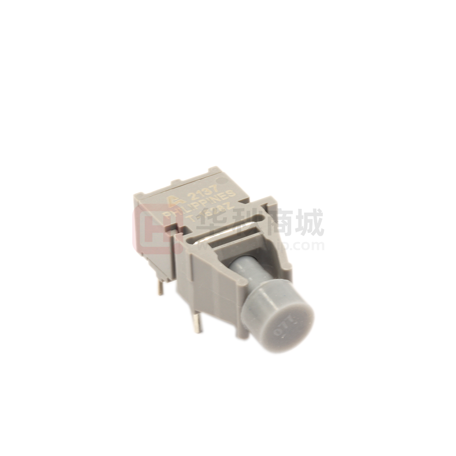
�HFBR-1528Z Transmitter
The HFBR-1528Z transmitter incorporates a 650 nm LED
in a light gray, nonconductive plastic housing. The high
light output power enables the use of both plastic optical
fiber (POF) and Hard Clad Silica (HCS) fiber. This transmitter can be operated up to 10 MBd using a simple driver
circuit. The HFBR-1528Z is compatible with all Versatile
Link connectors.
8 GROUND
ANODE
CATHODE
PT
Peak Output Power
1 mm POF, 20 mA
PT
Peak Output Power
200 μm HCS, 60 mA
PT
-6.0
-3.5
Peak Emission
Wavelength
Δ/ΔT
Spectral Width
FWHM
Forward Voltage
VF
Forward Voltage Temperature Coefficient
ΔVF /ΔT
Reverse Input Breakdown Voltage
VBR
Diode Capacitance
4
5 GROUND
HFBR-1528Z Transmitter, top view
0.0
dBm
TA (°C)
Conditions
Note
+25
IF, dc = 60 mA
2, 3
Fig. 2
IF,dc = 20 mA
2, 3
Fig. 2
IF,dc = 60 mA
2, 3
Fig. 2
0 to +70
+1.3
-40 to +85
-15.6
-9.0
-16.1
-2.0
dBm
-1.5
-8.5
+25
0 to +70
-0.7
-12.5
-40 to +85
dBm
+25
-17.0
-8.0
0 to +70
-17.3
-7.2
-40 to +85
640
-0.40
%/°C
-0.02
dB/°C
650
635
Peak Wavelength
Temperature
Coefficient
GROUND
+0.5
ΔPT /ΔT
P
3
-7.2
-16.8
Optical Power Temperature Coefficient
GROUND
-6.9
-16.5
660
nm
662
0.12
2.1
Fig. 3
0 to +70
-40 to +85
nm/°C
21
1.8
2
SEE NOTE 5
Electrical and Optical Characteristics: TA = -40° to +85°C unless otherwise noted.
Parameter
Symbol
Min.
Typ.[1]
Max.
Units
Peak Output Power
1 mm POF, 60 mA
1
nm
2.65
V
Fig. 3
IF,dc = 60 mA
-1.8
mV/°C
13
V
IF,dc = -10 μA
CO
60
pF
VF = 0 V,
f = 1 MHz
Transmitter
Numerical Aperture
NA
0.5
Thermal Resistance,
Junction to Case
jc
140
°C/W
Optical Rise Time
tr
13
ns
Optical Fall Time
tf
10
ns
3.0
Fig. 1
Fig. 1
4
10% to 90%,
IF = 60 mA
Notes:
1. Typical data are at 25°C.
2. Optical power measured at the end of 0.5 meters of 1 mm diameter plastic or 200 μm diameter hard clad silica fiber with a large area detector.
3. Minimum and maximum values for PT over temperature are based on a fixed drive current. The recommended drive circuit has temperature
compensation which reduces the variation in PT over temperature; refer to Figures 4 and 6.
4. Typical value measured from junction to PC board solder joint for horizontal mount package, HFBR-1528Z.
5. Pins 5 and 8 are for mounting and retaining purposes, but are electrically connected; pins 3 and 4 are electrically isolated. It is recommended
that pins 3, 4, 5 and 8 all be connected to ground to reduce coupling of electrical noise.
6. Refer to the “Plastic Optical Fiber and HCS Fiber Cable and Connectors for Versatile Link” Technical Data Sheet for cable connector options for 1
mm plastic and 200 μm HCS optical fiber.
3
�PT - NORMALIZED OUTPUT POWER - dB
2.5
VF - FORWARD VOLTAGE - V
-40° C
0° C
2.3
25° C
70° C
2.1
1.9
85° C
1.7
1.5
1
10
100
IF,DC - TRANSMITTER DRIVE CURRENT - mA
-40° C
0
25° C
-10
85° C
-20
-30
-40
1
10
100
IF,DC - TRANSMITTER DRIVE CURRENT - mA
Figure 2. Typical normalized optical power vs. drive current
1.2
1.4
-40° C
1.2
NORMALIZED OUTPUT POWER
NORMALIZED SPECTRAL OUTPUT POWER
Figure 1. Typical forward voltage vs. drive current
10
0° C
1.0
25° C
0.8
70° C
0.6
85° C
0.4
0.2
0
610
630
650
670
VCC = 5.25 V
1.1
VCC = 5.0 V
1.0
0.9
VCC = 4.75 V
0.8
0.7
-40
690
-20
0
40
20
80
60
TEMPERATURE - °C
WAVELENGTH - nm
Figure 4. Typical normalized optical power vs. temperature
(in recommended drive circuit)
Figure 3. Typical normalized optical spectra
VCC
C1
2
R1
C2
R2
1
1
PWD - ns
0
-1
VCC = 5.25 V
3
6
VCC = 5.0 V
8
DATA
VCC = 4.75 V
5
7
4
-4
0
4
5
1/2 SN75451
-3
-20
8
2
-2
-5
-40
HFBR-1528Z
20
40
60
80
TEMPERATURE - °C
Figure 5. Typical optical pulse width distortion vs. temperature
and power supply voltage (in recommended drive circuit)
VALUE
TOLERANCE
R1
2 KΩ
5%
R2
47Ω
1%
C1
0.1 μF
20 %
C2
1.0 μF
20 %
Figure 6. Recommended transmitter drive circuit
(IF,on = 60 mA nominal at TA = 25°C)
WARNING: WHEN VIEWED UNDER SOME CONDITIONS, THE OPTICAL PORT MAY EXPOSE THE EYE BEYOND THE MAXIMUM PERMISSIBLE EXPOSURE RECOMMENDED IN ANSI Z136.2, 1993. UNDER MOST VIEWING CONDITIONS THERE IS NO EYE HAZARD.
4
�HFBR-2528Z Receiver
GROUND 5
The HFBR-2528Z receiver consists of a silicon PIN photodiode and digitizing
IC to produce a logic compatible output. The IC includes a unique circuit to
correct the pulse width distortion (PWD) of the first bit after a long idle period. This enables operation from DC to 10 MBd with low PWD for arbitrary
data patterns.
The receiver output is a “push-pull” stage compatible with TTL and CMOS
logic. The receiver housing is a dark, conductive plastic, compatible with all
Versatile Link connectors.
4
3
IC
PRL,min
Peak POF Overdrive
Limit:Maximum
Input for Logic “0”
PRL,max
Peak POF Off State
Limit: Maximum
Input for Logic “1”
PRH,max
Peak HCS
Sensitivity: Minimum
Input for Logic “0”
PRL,min
Peak HCS Overdrive
Limit: Maximum
Input for Logic “0”
PRL,max
Peak HCS Off State
Limit: Maximum
Input for Logic “1”
PRH,max
-23.0
+1.0
+0.0
-1.0
+5.0
-25.0
-1.0
-2.0
-3.0
-21.0
-20.0
-19.5
19
GROUND
1
VO
SEE NOTES 5,7
HFBR-2528Z Receiver, top view
Note
Fig.
dBm
+25
0 to +70
-40 to +85
1 mm POF,
|PWD| < 30 ns
2,6
8,10
dBm
+25
0 to +70
-40 to +85
1 mm POF,
|PWD| < 30 ns
2,3,
6
7,8,
9
1 mm POF
2,6,
8
-42
dBm
-23.0
-22.0
-21.5
dBm
+25
0 to +70
-40 to +85
200 μm HCS,
|PWD| < 30 ns
2,6
dBm
+25
0 to +70
-40 to +85
200 μm HCS,
|PWD| < 30 ns
2,3,
6
200 μm HCS
2,6,
8
+3.0
-44
dBm
45
mA
VO = Open
V
IO = -40 μA
Supply Current
ICC
High Level Output
Voltage
VOH
Low Level Output
Voltage
VOL
0.22
0.4
V
IO = +1.6 mA
Output Rise Time
tr
12
30
ns
CL = 10 pF
6
Output Fall Time
tf
10
30
ns
CL = 10 pF
6
Thermal Resistance,
Junction to Case
jc
200
°C/W
Electric Field
Immunity
EMAX
8
V/m
Near Field,
Electrical
Field Source
5
Power Supply
Noise Immunity
PSNI
0.4
Vpp
Sine Wave
DC - 10 MHz
6
4.2
0.1
4.7
VCC
2
GROUND 8
Electrical and Optical Characteristics: TA = -40° to +85°C, 4.75 V < VCC < 5.25 V, unless otherwise noted.
Parameter
Symbol
Min.
Typ.[1]
Max.
Unit
TA (°C)
Condition
Peak POF Sensitivity:
Minimum Input for
Logic “0”
NO CONNECT
4
Notes:
1. Typical data are at +25°C, VCC = 5.0 V.
2. Input power levels are for peak (not average) optical input levels. For 50% duty cycle data, peak optical power is twice the average optical
power.
3. Receiver overdrive (PRL,max) is specified as the limit where |PWD| will not exceed 30 ns. The receiver will be in the correct state (logic “0”) for optical powers above PRL,max. However, it may not meet a 30% symbol period PWD if the overdrive limit is exceeded. Refer to Figure 8 for PWD performance at high received optical powers.
4. Typical value measured from junction to PC board solder joint for horizontal mount package, HFBR-2528Z.
5. Pins 5 and 8 are electrically connected to the conductive housing and are also used for mounting and retaining purposes. It is required that
pins 5 and 8 be connected to ground to maintain conductive housing shield effectiveness.
6. In recommended receiver circuit, with an optical signal from the recommended transmitter circuit.
7. Pin 4 is electrically isolated internally. Pin 4 may be externally connected to pin 1 for board layout compatibility with HFBR-25X1Z, HFBR-25X2Z
and HFBR-25X4Z. Otherwise it is recommended pin 4 be grounded as in Figure 11.
8. BER ≤ 10E-9, includes a 10.8 dB margin below the receiver switching threshold level (signal to noise ratio = 12).
5
�30
6
5
20
VCC = 5.0 V
RECEIVED PWD - ns
RECEIVED POWER - dBm
VCC = 5.25 V
4
VCC = 4.75 V
3
2
0
20
40
60
80
-10
-30
-22
100
TEMPERATURE - qC
9
-1
8
-2
7
-3
PWD - ns
0
6
-5
4
-6
4.9
5
5.1
5.2
-7
4.7
5.3
Figure 9. Typical POF receiver pulse width distortion vs. power
supply voltage at high optical power (0 dBm,pk, 10 MBd)
HFBR-2528Z
R1
4
3
IC
2
-2
2
VALUE
TOLERANCE
R1
2.7 :
5%
C1
0.1 μF
20 %
4.8
4.9
5
5.1
5.2
5.3
Figure 10. Typical POF receiver pulse width distortion vs. power
supply voltage at mid optical power, (-6 dBm,pk, 10 MBd)
VCC
C1
1
8
-6
VCC - VOLTS
VCC - VOLTS
5
-10
-4
5
4.8
-14
Figure 8. Typical POF receiver pulse width distortion vs. optical
power at 10 MBd
10
3
4.7
-18
PRL - RECEIVER OPTICAL INPUT POWER - dBm
Figure 7. Typical POF receiver overdrive, PRL,max, at 10 MBd, vs.
temperature and power supply voltage
PWD - ns
0
-20
1
0
-40 -20
Figure 11. Recommended receiver application circuit
6
10
DATA
�8 GND
3 VCC
PHOTODIODE FILTER
(REGULATOR)
TIA
DELAY
PIN
PHOTO
DIODE
1
Vo Data
THRESHOLD
GENERATOR
DATA
COMPARATOR
TTL OUTPUT
BUFFER
2 GND
CASE
5 GND
Figure 12. HFBR-2528Z receiver block diagram
Versatile Link Mechanical Dimensions
Versatile Link Printed Circuit Board Layout Dimensions
PIN NO.1 INDICATOR
7.62
(0.300)
2.0
(0.080)
2.54
(0.100)
6.5
(0.255)
1.01¡ (0.040) DIA.
10.2
(0.400)
5.1
(0.200)
18.9
(0.743)
0.64
(0.025)
1.27
(0.050)
2.5
(0.100)
0.64 (0.025) DIA.
NOTE: ALL DIMENSIONS IN MM (INCHES).
ALL DIMENSIONS ± 0.25 mm UNLESS
OTHERWISE SPECIFIED.
ELECTRICAL PIN FUNCTIONS
TRANSMITTER
PIN NO. HFBR-1528
1
2
3
4
5
8
ANODE
CATHODE
GROUND*
GROUND*
GROUND**
GROUND**
1
8
1.85 MIN.
(0.073)
0.51
(0.020)
1.73
(0.068)
2
7.62
(0.300)
5
3.81(0.150) MAX.
3.56 (0.140) MIN.
3.0
(0.118)
3
4.2
(0.165)
7.62
(0.300)
7.62
(0.300)
4
RECEIVER
HFBR-2528
SIGNAL, VO
GROUND
VCC (+5 V)
GROUND*
GROUND**
GROUND**
* NO INTERNAL CONNECTION,
GROUND CONNECTION RECOMMENDED.
** PINS 5 AND 8 CONNECTED INTERNALLY
TO EACH OTHER.
For product information and a complete list of distributors, please go to our website:
www.avagotech.com
Avago, Avago Technologies, and the A logo are trademarks of Avago Technologies in the United States and other countries.
Data subject to change. Copyright © 2005-2011 Avago Technologies. All rights reserved. Obsoletes 5989-4632EN
AV02-1504EN - November 4, 2011
TOP VIEW
�


 工商网监
湘ICP备2023018690号
工商网监
湘ICP备2023018690号
