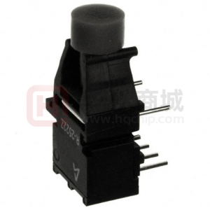
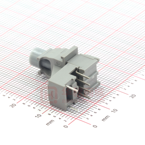
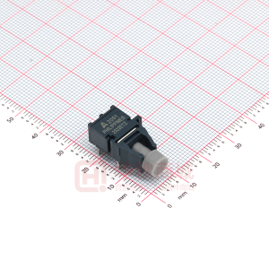
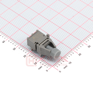
HFBR-7924Z
Four-Channel Pluggable Parallel Fiber Optic Transceiver Part of the Avago Technologies METRAK family
Data Sheet
Description The HFBR-7924Z transceiver is a high performance fiber optic module for parallel optical data communication applications. It incorporates 8 independent data channels (4 for transmit and 4 for receive) operating from 1 to 2.7 Gb/s per channel providing a cost effective solution for very short reach applications requiring 10.8 Gb/s aggregate bandwidth. The module is designed to operate on multimode fiber systems at a nominal wavelength of 850 nm. It incorporates high performance, highly reliable, short wavelength optical devices coupled with proven circuit technology to provide long life and consistent service. The HFBR-7924Z transceiver module incorporates a 4 channel VCSEL (Vertical Cavity Surface Emitting Laser) array together with a custom 4 channel laser driver integrated circuit providing IEC-825 and CDRH Class 1M laser eye safety. It also contains a 4 channel PIN photodiode array coupled with a custom preamplifier / post amplifier integrated circuit. Operating on 3.3 V power supply this module provides LVTTL/LVCMOS control interfaces and CML compatible high speed data lines which simplify external circuitry. The transceiver is housed in MTP®/MPO receptacled package with integral finned heatsink. Electrical connections to the device are achieved by means of a pluggable 10x10 connector array. Ordering Information The HFBR-7924Z product is available for production orders through the Avago Technologies Component Field Sales Office. HFBR-7924Z HFBR-7924EZ HFBR-7924HZ No EMI Nose Shield With Extended EMI Nose Shield No heatsink, No EMI Nose Shield
Features • RoHS Compliant • Four Transmit and Four Receive Channels; 1 to 2.7 GBd per channel • Compatible with SONET scrambled and 8B10B encoded data formats • 850 nm VCSEL array source • Conforms to “POP4” Four-Channel Pluggable Optical Transceiver Multisource Agreement • 50/125 µm multimode fiber operation • Distance up to 300 m with 500 MHz.km fiber at 2.5 Gb/s • Distance up to 600 m with 2000 MHz.km fiber at 2.5 Gb/s • Pluggable package • Outputs (Tx & Rx) are squelched for loss of signal • Control I/O is compatible with LVTTL and LVCMOS • Standard MTP® MPO ribbon fiber connector interface • Integrated heat sink • Manufactured in an ISO 9002 certified facility • Rx Signal Detect Applications • Telecom and Datacom Switch/Router Rack-to-Rack Connections • OC-192 Very Short Reach (VSR), OIF-VSR4-03.0, Interconnects • Computer Cluster Interconnects
HFBR-7924EHZ No heatsink, with EMI Nose Shield
�DIN Ch 0 - 3 +
4 Channels Input Stage Driver VCSEL Array
ode ber Bar Crt Num Pa
POINT FOR TAKING MODULE TEMPERATURE
DIN Ch 0 - 3 -
TX_DIS TX_EN TX_FAULT* TX_RESET* SD
Control
Vcc_TX GND_TX Vcc_RX GND_RX
Figure 2 - Case temperature measurement
25
Module Case Temperature Rise Above Ambient (oC)
20 15 10 5 0 0 0.5 1 Air Velocity (m/s) 1.5 2
DOUT Ch 0 - 3 + Driver DOUT Ch 0 - 3 -
4 Channels Input Stage
PIN Array
Figure 1 - Block Diagram (dimensions in mm) Figure 3 - Ambient air temperature and air flow for TC = +80 °C
2
�Package Dimensions
Notes: 1. Module mass approximately 20 grams. Figure 4A - HFBR-7924Z Package dimensions (dimensions in mm)
Figure 4B - HFBR-7924EZ Package dimensions (dimensions in mm)
3
�Figure 5A - HFBR-7924HZ Package Dimensions (dimensions in mm)
Figure 5B - HFBR-7924EHZ Package Dimensions (dimensions in mm)
4
�2 x ∅2.54 MIN. PAD KEEP-OUT ∅0.1 A B-C 2 x∅ 1.7 ± 0.05 HOLES ∅ 0.1 A B-C 3 x ∅4.17 MIN. PAD KEEP-OUT ∅0.1 A B-C 3 x ∅2.69 ± 0.05 HOLES FOR #2 SCREW ∅0.1 A B-C 6.73 B A
SYM.
13.72
18 REF.
18.42 MIN.
100 PIN FCI MEG-Array® RECEPTACLE CONNECTORS C SYM. 9 x 1.27 TOT = 11.43
FRONT
END OF MODULE (10 x 10 =) 100 x ∅ 0.58 ± 0.05 PADS ∅ 0.05 A B-C 6.73
50 KEEP-OUT AREA FOR MPO CONNECTOR 8.95 REF. 30.23 PCB TOP VIEW
9 x 1.27 TOT = 11.43 1.89 REF.
NOTE: The host electrical connector attached to the PCB must be a 100-position FCI Meg-Array® Pao-Ann to provide changes or equivalent. Figure 6 - Package Board Footprint (dimensions in mm)
19.02 min
0.50 max Front Panel
3.60 ± 0.2
PCB 15.70 ± 0.25
13.40 ± 0.2
PCB
35.31+/- 0.20
Figure 7 - Host Frontplate Layout (dimensions in mm)
5
�Absolute Maximum Ratings
Stresses in excess of the absolute maximum ratings can cause catastrophic damage to the device. Limits apply to each parameter in isolation, all other parameters having values within the recommended operating conditions. It should not be assumed that limiting values of more than one parameter can be applied to the product at the same time. Exposure to the absolute maximum ratings for extended periods can adversely affect device reliability.
Parameter
Storage Temperature Supply Voltage Data/Control Signal Input Voltage Transmitter Differential Input Voltage Output Current (dc) Relative Humidity (Non Condensing)
Symbol
TS VCC VI | VD | ID RH
Minimum
-40 -0.5 -0.5
Maximum
+100 4.6 VCC + 0.5 2 25
Unit
ºC V V V mA %
Reference
1
5
95
Recommended Operating Conditions
Recommended Operating Conditions specify conditions for which the optical and electrical characteristics hold. Optical and electrical characteristics are not specified for operation beyond the Recommended Operating Conditions, reliability is not implied and damage to the device may occur for such operation over an extended time period.
Parameter
Case Temperature Supply Voltage Signaling Rate/Channel Data Input Differential Peak-to-Peak Voltage Swing Data Input Rise & Fall Time (20-80%) Control Input Voltage High Control Input Voltage Low Power Supply Noise Data I/O Coupling Capacitors Receiver Differential Data Output Load
Symbol
TC VCC
Minimum Typical
0 3.135 1 3.3
Maximum Unit
+80 3.465 2.7 1600 160 ºC V GBd mVP-P ps V V mVP-P µF W
Reference
2, Figures 2, Figure 8
DVDINP-P tr, tf VIH VIL NP CAC RDL
175
3, Figures 11,12
2.0 VEE
VCC 0.8 200 0.1 100
4, Figure 8 5, Figure 9 Figure 9
Notes: 1. This is the maximum voltage that can be applied across the Transmitter Differential Data Inputs without damaging the input circuit. 2. Case Temperature is measured as indicated in Figure 2. 3. Data inputs are CML compatible. Coupling capacitors are required to block dc. DVDIN p-p = DVDINH - DVDINL, where DVDINH = High State Differential Data Input Voltage and DVDINL = Low State Differential Data Input Voltage. 4. Power Supply Noise is defined at the supply side of the recommended filter for all VCC supplies over the frequency range from 500 Hz to 2700 MHz with the recommended power supply filter in place. 5. For data patterns with restricted run lengths, e.g. 8B10B encoded data, smaller value capacitors may provide acceptable results.
6
�Transmitter Electrical Characteristics (Over recommended operating conditions: Tc= 0ºC to +80ºC, Vcc=3.3V + 5%)
Parameter
Differential Input Impedance FAULT* Assert time RESET* Assert time RESET* De-assert time Transmit Enable (TX_EN) Assert time Transmit Enable (TX_EN) De-assert time Transmit Disable (TX_DIS) Assert time Transmit Disable (TX_DIS) De-assert time Power-On Initiation Time Control I/Os TX _DIS, TX_EN, TX_FAULT*, TX_RESET* Input Current High Input Current Low Output Voltage Low Output Voltage High | IIH | | IIL | VOL VOH VEE 2.4
Symbol
Zin TOFF TOFF TON TON TOFF TOFF TON
Minimum Typical
80 100
Maximum Unit
120 100 7.5 18 18 7.5 7.5 18 W µs µs ms ms µs µs ms ms 0.5 0.5 0.4 VCC mA mA V V
Reference
6, Figure 9 Figure 13 Figure 14 Figure 14 Figure 15 Figure 15 Figure 15 Figure 15 Figure 17 2.0 V < VIH < VCC VEE < VIH < 0.8 V IOL = 4.0 mA IOH = -0.5 mA
21
Transmitter Optical Characteristics (Over recommended operating conditions: Tc= 0ºC to +80ºC, Vcc=3.3V + 5%)
Parameter
Output Optical Power 50/125 µm, Fiber NA = 0.2 Extinction Ratio Center Wavelength Spectral Width - rms Rise, Fall Time Inter-channel Skew Relative Intensity Noise Deterministic Jitter Contribution Total
Symbol
POUT ER lC s tr, tf
Minimum Typical
-8.0 6 830 -4.5 7.5 850
Maximum Unit
-2.0 dBm avg. dB 860 0.85 nm nm rms ps ps dB/Hz psp-p psp-p
Reference
7 8
60 50
150 100 -121 50 120
9 10
RIN DJ TJ
-127 20 45
11 12
Notes: 6. Differential impedance is measured between DIN+ and DIN- over the range 4 MHz to 2 GHz. 7. The specified optical output power, measured at the output of a 2 meter test cable, will be compliant with IEC 60825-1 Amendment 2, Class 1M Accessible Emission Limits, AEL Regulatory Compliance section. 8. Extinction Ratio is defined as the ratio of the average output optical power of the transmitter in the high (“1”) state to the low (“0”) state and is expressed in decibels (dB) by the relationship 10log(Phigh avg/Plow avg). The transmitter is driven with a 550 MBd, 101010 pattern. 9. These are unfiltered 20% - 80% values measured with a 550 MBd 101010 pattern. 10. Inter-channel Skew is defined for the condition of equal amplitude, zero ps skew input signals. 11. Deterministic Jitter (DJ) is defined as the combination of Duty Cycle Distortion (Pulse-Width Distortion) and Data Dependent Jitter. Deterministic Jitter is measured at the 50% signal threshold level using a 2500 MBd Pseudo Random Bit Sequence of length 223-1 (PRBS-23), or equivalent, test pattern with zero skew between the differential data input signals. 12. Total Jitter (TJ) includes Deterministic Jitter and Random Jitter (RJ). Total Jitter is specified at a BER of 10-12 for the same 2.5 GBd test pattern as for DJ and is measured with all channels operating.
7
�Receiver Electrical Characteristics (Over recommended operating conditions: Tc= 0ºC to +80ºC, Vcc=3.3V + 5%)
Parameter
Differential Output Impedance Data Output Differential Peak-to-Peak Voltage Swing Inter-channel Skew Data Output Rise, Fall Time Control I/O Signal Detect LVTTL & LVCMOS Compatible Output Voltage Low Output Voltage High Assert Time (OFF-to-ON) De-assert Time (ON-to-OFF) tr, tf VOL VOH tSDA tSDD VEE 2.4 50 50
Symbol
ZOUT DVDOUTP-P
Minimum Typical
100 500 650 50 120
Maximum Unit
W 800 100 150 0.4 VCC mVP-P ps ps V V µs µs
Reference
13, Figure 9 14, Figure 10 15 16 IOL = 4.0 mA IOH = -0.5 mA 17 18
Receiver Optical Characteristics (Over recommended operating conditions: Tc= 0ºC to +80ºC, Vcc=3.3V + 5%)
Parameter
Input Optical Power - Sensitivity Input Optical Power - Saturation Operating Center Wavelength Stressed Receiver Sensitivity Stressed Receiver Eye Opening Return Loss Asserted Signal Detect Deasserted Hysteresis PA PD PA - PD -31 0.5 111 12 -22 -27 1.0 -17
Symbol
PIN MIN PIN MAX lC
Minimum Typical
-18 -2.0 830
Maximum Unit
-16.0 dBm avg. dBm avg. 860 -11.7 nm dBm ps dB dBm avg. dBm avg. dB
Reference
19
20 21 22 23
Notes: 13. Measured over the range 4 MHz to 2 GHz. 14. DVDOUTP-P = DVDOUTH - DVDOUTL, where DVDOUTH = High State Differential Data Output Voltage and DVDOUTL = Low State Differential Data Output Voltage. DVDOUTH and DVDOUT L = VDOUT+ - VDOUT -, measured with a 100 W differential load connected with the recommended coupling capacitors and with a 2500 MBd, 101010 pattern. 15. Inter-channel Skew is defined for the condition of equal amplitude, zero ps skew input signals. 16. Rise and Fall Times are measured between the 20% and 80% levels using a 550 MHd square wave signal. 17. The Signal Detect output will change from logic “0” (Low) to “1” (High) within the specified assert time for a step transition in optical input power from the deasserted condition to the specified asserted optical power level. 18. The Signal Detect output will change from logic “1” (High) to “0” (Low) within the specified de-assert time for a step transition in optical input power from the specified asserted optical power level to the deasserted condition. 19. Sensitivity is defined as the average input power with the worst case, minimum, Extinction Ratio necessary to produce a BER < 10-12 at the center of the Baud interval. For this parameter, input power is equivalent to that provided by an ideal source, i.e. one with RIN and switching attributes that do not degrade the sensitivity measurement. All channels not under test are operating receiving data with an average input power of up to 6 dB above PIN MIN. Sensitivity at signal rates from 1 to 2.7 GBd is defined for a PRBS 223-1 test pattern. 20. The stressed receiver sensitivity is measured using 2.6 dB Inter-Symbol Interference, ISI, (min), 30 ps Duty Cycle Dependent Deterministic Jitter, DCD DJ (min) and 6 dB ER (ER Penalty = 2.23 dB). All channels not under test are operating receiving data with an average input power of up to 6 dB, above PIN MIN. 21. The stressed receiver eye opening is measured using 2.6 dB ISI (min), 30 ps DCD DJ (min), 6 dB ER (ER Penalty = 2.23 dB) and an average input optical power of -11.7 dBm. All channels not under test are operating receiving data with an average input power of up to 6 dB above PIN MIN. 22. Return loss is defined as the ratio, in dB, of the received optical power to the optical power reflected back down the fiber. 23. Signal Detect assertion requires all optical inputs to exhibit a minimum 6 dB Extinction Ratio at PA = -17 dBm. All channels not under test are operating with PRBS 223-1patterns, asynchronous with the channel under test, and average input power of up to 6 dB above the specified PIN MIN.
8
�General/Control Electrical Characteristics (Over recommended operating conditions: Tc= 0ºC to +80ºC, Vcc=3.3V + 5%)
Parameter
Supply Current Power Dissipation
Symbol
ICCT PDIST
Minimum Typical
300 1.0
Maximum Unit
400 1.39 mA W
Reference
Regulatory Compliance The overall equipment design will determine the certification level. The module performance is offered as a figure of merit to assist the designer in considering their use in equipment designs. Electrostatic Discharge (ESD) There are two design cases in which immunity to ESD damage is important. The first case is during handling of the module prior to mounting it on the circuit board. It is important to use normal ESD handling precautions for ESD sensitive devices. These precautions include using grounded wrist straps, workbenches and floor mats in ESD controlled areas. The module performance has been shown to provide adequate performance in typical industry production environments. The second case to consider is static discharges to the exterior of the equipment chassis containing the module parts. To the extent that the MT-based connector receptacle is exposed to the outside of the equipment chassis it may be subject to whatever system-level ESD test criteria that the equipment is intended to meet. The module performance exceeds typical industry equipment requirements of today. Electromagnetic Interference (EMI) Most equipment designs using these high-speed modules from Avago Technologies will be required to meet the requirements of FCC in the United States, CENELEC EN55022 (CISPR 22) in Europe and VCCI in Japan. These modules, with their shielded design, perform to the limits listed in Table 1 to assist the designer in the management of the overall equipment EMI performance.
Immunity Equipment utilizing these modules will be subject to radio frequency electromagnetic fields in some environments. These modules have good immunity to such fields due to their shielded design. Eye Safety These 850 nm VCSEL-based transceiver modules provide eye safety by design. The HFBR-7924Z has been registered with CDRH and certified by TUV as a Class 1M device under Amendment 2 of IEC 60825-1. See the Regulatory Compliannce Table for further detail. If Class 1M exposure is possible, a safety-warning label should be placed on the product stating the following: LASER RADIATION DO NOT VIEW DIRECTLY WITH OPTICAL INSTRUMENTS. CLASS 1M LASER PRODUCT MTP®(MPO) Optics Cleaning Statement The optical port has recessed optics that are visible through the nose of the port. The port plug provided should be installed whenever a fiber cable is not connected. This ensures the optics remain clean and no cleaning should be necessary. In the event of the optics being contaminated, forced nitrogen or dry clean air at less than 20 psi is the recommended cleaning agent. The features of the optical port and guide pins preclude the use of any solid instrument. Liquids are not advised due to potential damage. Application of wave soldering, reflow soldering and/or aqueous wash processes with the HFBR-7924Z modules device on board is not recommended as damage may occur. Normal handling precautions for electrostatic sensitive devices should be taken (see ESD section).
9
�Table 1 - Regulatory Compliance
Feature
Electrostatic Discharge (ESD to the Electrical Pads) Electrostatic Discharge (ESD to the Connector Receptacle) Electromagnetic Interference (EMI) Immunity Laser Eye Safety and Equipment Type Testing Component Recognition FCC Class B CENELEC EN55022 Class B (CISPR 22A) VCCI Class 1 Variation of IEC 61000-4-3 IEC 60825-1 Amendment 2 CFR 21 Section 1040 Underwriters Laboratories and Canadian Standards Association Joint Component Recognition for Information Technology Equipment Including Electrical Business Equipment. RoHS Complaince Less than 1000ppm of Cadmium, lead, mercury, hexavalent chromium, polybrominated biphenyls, and polybrominated biphenyl ethers
Test Method
JEDEC Human Body (HBM) (JESD22-A114B) JEDEC Machine Model (MM) Variation of IEC 61000-4-2
Performance
Module > 1000 V Module > 50 V Typically withstand at least 6 kV (module biased) without damage when the connector receptacle is contacted by a Human Body Model probe Typically pass with 5 dB margin. (See Notes 24 and 25) Typically show no measurable effect from a 10 V/m field swept from 80 MHz to 1 GHz applied to the module without a chassis enclosure. IEC AEL & US FDA CDRH Class 1M CDRH Accession Number: 9720151-22 TUV Bauart License: E2171095.04 UL File Number: E173874
Notes: 24. EMI performance only refers to shielded version HFBR-7924EZ and HFBR-7924EHZ. 25. EMI performance could be improved by connecting the following pads to electrical ground : C9, G7 and H9.
10
�4+4 Transceiver Module Pad Assignment - HFBR-7924Z
K 1 DOUT00-
J
H
G
F VEE RX
E VEE TX
D VEE TX
C DIN03-
B VEE TX
A DIN00+
VEE RX DOUT03+ VEE RX
2 DOUT00+
VEE RX
DOUT03-
VEE RX
VEE RX
VEE TX
VEE TX
DIN03+
VEE TX
DIN00-
3
VEE RX
VEE RX
VEE RX
VEE RX
VEE RX
VEE TX
VEE TX
VEE TX
VEE TX
VEE TX
4
DOUT1+
VEE RX
DOUT02-
DNC
DNC
DNC
DNC
DIN02+
VEE TX
DIN01-
5
DOUT1-
VEE RX DOUT02+
DNC
DNC
DNC
DNC
DIN02-
VEE TX
DIN01+
6
VEE RX
VEE RX
VEE RX
DNC
DNC
DNC
DNC
VEE TX
VEE TX
VEE TX
7
VCCB RX VCCB RX VCCB RX
DNC
DNC
DNC
DNC
VCC TX
VCC TX
VCC TX
8
DNC
Reserved Reserved Reserved TBD MSA TBD MSA TBD MSA Reserved Reserved TBD MSA TBD MSA VEE RX SD
DNC
TX_DIS
TX_EN
DNC
DNC
DNC
9
DNC
DNC
RESET*
FAULT*
DNC
DNC
DNC
10
VCCA RX VCCA RX
DNC
DNC
DNC
DNC
VEE TX
VCC TX
VCC TX
TOP VIEW (PCB LAYOUT) (10 x 10 ARRAY)
11
�Table 2. Transceiver Module Pad Description
Symbol
Din Ch 0 - 3 +/- through Din Ch 0 - 3 +/TX_DIS
Functional Description
Transmitter differential data inputs for channels 0 through 3: Data inputs are CML compatible.
Transmitter Disable: LVCMOS Input (Internal pull down). Control input used to turn off the transmitter optical outputs. High Active. VCSEL array is off when High. Normal operation is enabled when Low. Transmitter Enable: LVCMOS Input (Internal pull up). Control input used to enable the transmitter optical outputs. High Active. VCSEL array is off when Low. Normal operation is enabled when High. Transmitter Fault: LVCMOS Output. Transmitter status output indicating an eye-safety over-current condition for any VCSEL, an out of temperature range condition and/or a calibration data corruption detection. High output state indicates normal operation. Low output state indicates the fault condition. An asserted FAULT* condition disables the VCSEL array and is cleared by TX_RESET*. Transmitter Reset: LVCMOS Input (Internal pull up). Control input used to reset the transmitter logic functions. Active Low. VCSEL array is off when Low. Normal operation is enabled when High. Transmitter signal common. All transmitter voltages are referenced to this potential unless otherwise stated. Directly connect these pads to the PC board transmitter ground plane. Transmitter power supply. Receiver differential data outputs for channels 0 through 3: Data outputs are CML compatible. Data outputs are squelched for de-asserted Signal Detect. Receiver Signal Detect: LVCMOS Output. Receiver status output indicating valid signal in all channels. High output state (asserted) indicates valid optical inputs to each and every channel. Low output state (de-asserted) indicates loss of signal at any of the monitored receiver inputs. All channels are monitored. Do NOT Connect. Do not connect to any electrical potential. Receiver signal common. All receiver voltages are referenced to this potential unless otherwise stated. Directly connect these pads to the PC board receiver ground plane. Pin preamplifier power supply rail. Receiver quantizer power supply rail.
TX_EN
TX_FAULT*
TX_RESET*
VEE_TX VCC_TX Dout Ch 0 - 3 +/- through Dout Ch 0 - 3 +/SD
DNC VEE_RX VCCA_RX VCCB_RX
VCCA_RX and VCCB_RX can be connected to the same power supply. However, to insure maximum receiver sensitivity and minimize the impact of noise from the power supply, it is recommended to keep the power supplies separate and to use the recommended power supply filtering network on VCCA_RX (see Figure 8). Module Case Transceiver Case Common. Transceiver Case Common incorporates all exposed conductive surfaces and is electrically isolated from Transmitter Signal Common and Receiver Signal Common.
12
�HFBR-7924Z R6 1.0 k Ω 0603 Vcc Tx L6 6.8 nH 0805 Vcc Tx Vcc Tx Vcc Tx C12 0.1 µF 0603 C11 0.1 µF 0603 C10 10 µF 1210 C9 10 µF 1210 L5 1 µH 2220 R5 100 Ω 0603 VCC
R4 1.0 k Ω 0603 VccA Rx L4 6.8 nH 0805 VccA Rx C8 0.1 µF 0603 C7 0.1 µF 0603 C6 10 µF 1210
R3 100 Ω0603 L3 1 µH 2220 C5 10 µF 1210 VCC
R2 1.0 k Ω 0603 VccB Rx L2 6.8 nH 0805 VccB Rx VccB Rx C4 0.1 µF 0603 C3 0.1 µF 0603 C2 10 µF 1210
R1 100 Ω 0603 VCC L1 1 µH 2220 C1 10 µF 1210
Figure 8 - Recommended power supply filter
13
�DOUT+
CAC RDL
DIN+
RECEIVER
ZIN
DOUT-
CAC
DIN-
AC COUPLING CAPACITORS (DC BLOCKING CAPACITORS) SHOULD BE USED TO CONNECT DATA OUTPUTS TO THE LOAD. THE DIFFERENTIAL DATA PAIR SHOULD BE TERMINATED WITH A DIFFERENTIAL LOAD, RDL, OF 100 Ω USING EITHER AN INTERNAL LOAD, ZIN, AS SHOWN ABOVE, OR AN EXTERNAL LOAD, IF NECESSARY. Figure 9 - Recommended AC coupling and data signal termination
DIN+ + ∆VDIN DINTRANSMITTER ∆VDI/OH
VDI/O +
∆VDI/OL
VDI/O DOUT+ + RECEIVER ∆VDOUT O D∆UT∆VDI/OH + ∆VDI/O P-P VDI/O REFERS TO EITHER VDIN OR VDOUT AS APPROPRIATE. ∆VDI/OL -
Figure 10 - Differential signals
VCC
VCCT DIN+ 50 Ω ZIN 50 Ω DINVEE VBIAS (N ONIMAL 1.9V)
50 Ω
50 Ω DOUT+
DOUT-
VEE
Figure 11 - Transmitter data input equivalent circuit
Figure 12 - Receiver data output equivalent circuit.
14
�NO FAULT DETECTED
FAULT DETECTED
< 100 µs
~ 100 ns
FAULT*
TX OUT Ch 0 - 3 Figure 13 - Transmitter FAULT* signal timing diagram
RESET*
FAULT* >100 ns 18 ms (max) ~4.2 ms
TX_OUT Ch 0
SHUTDOWN ~4.6 ms (typ)
NORMAL
TX_OUT Ch 1
TX_OUT Ch 2
TX_OUT Ch 3 7.5 µs (max)
Figure 14 - Transmitter RESET* timing diagram
15
�TX_EN ~ 7.5 µs TX OUT Ch 0 - 3 Normal (a) Shutdown
TX_DIS ~ 7.5 µs TX OUT Ch 0 - 3 Normal (b) NOTE [1]: TX_DIS, WHICH IS NOT SHOWN, IS THE FUNCTIONAL COMPLEMENT OF TX_EN. Shutdown
TX_EN [1]
~18 ms ~4.2 ms ~4.6 ms
TX OUT Ch 0 TX OUT Ch 1 TX OUT Ch 2 TX OUT Ch 3 (c)
Figure 15 - Transmitter TX_EN and TX_DIS timing diagram
> 1 ms ~18 ms ~ 200 ns ~4.2 ms ~4.6 ms
TX_EN [1]
FAULT*
Tx OUT Ch 0
Tx OUT Ch 1
Tx OUT Ch 2
Tx OUT Ch 3 NOTE [1]. TX_DIS, WHICH IS NOT SHOWN, IS THE FUNCTIONAL COMPLEMENT OF TX_EN.
Figure 16 - Transmitter fault recovery via TX_EN timing diagram
16
�Vcc > 2.8V Vcc ~21 ms 6.5ms NORMAL TX_OUT 0 TX_OUT 1 TX_OUT 2 TX_OUT 3 ~4.6ms ~4.6ms ~4.6ms NORMAL NORMAL NORMAL
Figure 17. Typical Transmitter Power-Up Sequence
For product information and a complete list of distributors, please go to our web site: www.avagotech.com Avago, Avago Technologies, and the A logo are trademarks of Avago Technologies, Pte. in the United States and other countries. Data subject to change. Copyright © 2006 Avago Technologies Pte. All rights reserved. AV01-0053EN - March 15, 2006
17
�